This material is posted here with permission of the IEEE. Internal or personal use of this material is permitted. However, permission to reprint/republish this material for advertising or promotional purposes or for creating new collective works for resale or redistributionmust be obtained from the IEEE by writing to
[email protected]. By choosing to view this document, you agree to all provisions of the copyright laws protecting it.
IEEE TRANSACTIONS ON NUCLEAR SCIENCE, VOL. 55, NO. 4, AUGUST 2008
2013
Use of Code Error and Beat Frequency Test Method to Identify Single Event Upset Sensitive Circuits in a 1 GHz Analog to Digital Converter Kirby Kruckmeyer, Member, IEEE, Robert L. Rennie, Member, IEEE, and Vishwanath Ramachandran
Abstract—Typical test methods for characterizing the single event upset performance of an analog to digital converter (ADC) have involved holding the input at static values. As a result, output error signatures are seen for only a few input voltage and output codes. A test method using an input beat frequency and output code error detection allows an ADC to be characterized with a dynamic input at a high frequency. With this method, the impact of an ion strike can be seen over the full code range of the output. The error signatures from this testing can provide clues to which area of the ADC is sensitive to an ion strike. Index Terms—Analog–digital conversion, beat frequency, code error, single event upset.
I. INTRODUCTION
C
HARACTERIZING the single event upset (SEU) signatures of a high speed mixed-signal product, such as an analog to digital converter (ADC), presents a unique challenge. For data converters with data rates at 1 gigasample per second (GS/s), just monitoring the outputs and recognizing output errors can be complex. To simplify the data collection, SEU testing of ADC’s has traditionally been done with the input held at a static value [1]–[3]. However, this only provides a snapshot of the upset signature at one input voltage and one output code. A test method has been previously demonstrated using a beat frequency and code error detection software so that an ADC could be tested with the input frequency close to 2 times Nyquist [4]. Using this method, the SEU signatures could be characterized over the full-scale input range and all output codes. This test method was demonstrated on National Semiconductor’s ADC08D1000WG-QV, a dual channel, 8 bit, low power ADC [5]. This paper will discuss the SEU signatures and how they were used to isolate which areas of the ADC08D1000WG-QV circuit are sensitive to an ion strike, resulting in long events, lasting over 100 ns. II. DEVICE DESCRIPTION
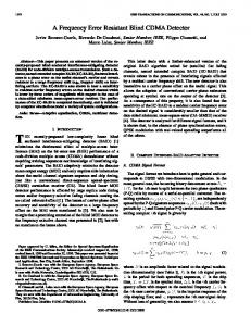
National Semiconductor’s ADC08D1000WG-QV is a dual channel 8 bit ADC that can run up to data rates of 1.2 gigasamManuscript received September 5, 2007; revised February 27, 2008. Published September 19, 2008. K. Kruckmeyer and R. L. Rennie are with National Semiconductor, Santa Clara, CA 95052 USA (e-mail:
[email protected]; rob.rennie@nsc. com). V. Ramachandran is with Vanderbilt University, Nashville, TN 37235 USA (e-mail:
[email protected]). Digital Object Identifier 10.1109/TNS.2008.921940
ples per second (GS/s) and supports input bandwidths to 1.7 GHz. It is built on a folding architecture for low power consumption (800 mW per channel) and uses a calibration circuit for improved performance with an effective number of bits (ENOB) of 7.2 at Nyquist [5]. Upon power up of the ADC08D1000WG-QV, a one time calibration based on an internal reference voltage is performed on the preamplifier offsets of each ADC bank. Fig. 1 shows the block diagram of the part, indicating the calibration circuit and input to the preamplifiers in the ADC banks. A more in depth discussion of the folding architecture and the operation of the calibration circuit is provided in [6]. The two channels (called I and Q) of the product operate independently, but share some common circuitry, such as the clock, control and reference circuits (Fig. 1). Each channel has a differential input and a 1:2 demultiplexed, parallel low voltage differential signaling (LVDS) output. In order to support the very high data conversion rates while maintaining a high ENOB, each channel is split into two interleaved signal conversion paths, after the input multiplexer (MUX), starting at the track and hold (T/H) (Fig. 1). Each signal conversion path runs at half the input clock speed, allowing for the track and hold times to be more than doubled (when including the impact of switching time) [6]. The ADC clock output is also at half the speed of the clock input. For instance, the I channel is separated into the DI and DId paths (Fig. 1). The output of the I channel is on two parallel LVDS buses (DI and DId) running at half the input clock speed. With the input clock at 1 GHz and sample rate at 1 GS/s, the output clock is 500 MHz. The DId output is delayed by one input clock cycle and the DI and DId outputs are clocked out together on the same output clock edge. III. TEST METHOD The code error and beat frequency test method used in this study is described in detail in [4]. ADC08D1000WG-QV die, assembled in plastic packages for this study, were decapped and soldered to ADC08D1000DEV boards [4]. Three separate units and boards were used for the testing. The ADC08D1000DEV board contains a Xilinx Virtex4 FPGA programmed with code error detection software. For each channel of the ADC, the Virtex4 monitored the output, compared it to the previous output and registered an error if the difference is more than some preset value (Fig. 2). For this testing, the threshold for an error to be registered was set at least significant bit (LSB), based on the high background
0018-9499/$25.00 © 2008 IEEE
2014
IEEE TRANSACTIONS ON NUCLEAR SCIENCE, VOL. 55, NO. 4, AUGUST 2008
Fig. 1. ADC08D1000WG-QV block diagram. It is a dual channel (I and Q) ADC. Each channel splits into two interleaved signal conversion paths, starting at the track and hold (T/H). The output of each channel is two interleaved 8 bit LVDS buses, DI and DId for the I channel and DQ and DQd for the Q channel. Upon power up, the preamplifier offsets of each ADC bank are calibrated.
Fig. 2. The code error detection software calculates the difference in the output codes between the two parallel LVDS output buses; DId and DI in the case of the I channel. If the difference is greater than a preset value, an error will be registered. With a 1 GHz input clock frequency and a 1.24 MHz output frequency, the maximum change between outputs is 1 LSB at the steepest part of the output sine wave.
noise due to the less than ideal conditions at the test facility [4]. For instance, on the I channel, the DI output code would be compared to the previous DId output code and an error would be registered if the magnitude of the difference of the output codes was greater than 6 LSB. The clock cycle, DI output code and previous DId code output would be recorded for the error. In order for the code error detection software to be effective, the expected output of the ADC cannot change by more than 1 LSB per clock cycle, otherwise invalid errors, on top of the background noise, would be recorded. For a 1 GS/s rate, the output frequency cannot be more than 1.24 MHz for a 1 LSB change at the steepest part of the output sine wave [4], [8].
Fig. 3. Beat frequency. With the clock frequency set at 1 GHz, and the input frequency, slightly lower at 998.76 MHz, the sampled points on the input curve will result in an output of 1.24 MHz.
So that the input of the ADC can be exercised at high bandwidths (nearly two times Nyquist), a beat frequency is used. A beat frequency (and the resultant output of the ADC) is the difference between the sampling frequency and the input frequency (Fig. 3). In this case, with the sampling frequency (and input clock) at 1 GHz, the input frequency was set at 998.76 MHz to achieve an output frequency of 1.24 MHz. Testing was done using the 88” cyclotron at the Berkeley Accelerated Space Effect facility at the Lawrence Berkeley National Laboratory. The 4.5 MeV/nucleon beam was used [9]. Ions used, linear energy transfers (LET) and penetration range into silicon are shown in Table I. For the ADC08D1000WG-QV, from the top of the upper passivation layer, through the metal
KRUCKMEYER et al.: USE OF CODE ERROR AND BEAT FREQUENCY TEST METHOD
2015
TABLE I LIST OF IONS USED, RAW ERROR COUNT AND NUMBER OF UPSET EVENTS FOR UNIT 2
layers, active areas and epi to the substrate is less than 11 microns. IV. ISOLATION OF SENSITIVE CELLS During an ion run, the code error detection software would record every clock cycle where the magnitude of the difference between the current output code and the previous output code was greater than 6 LSB. For an event that lasted one clock cycle, two “errors” would be recorded; one for the actual error and one for when the output returned to the expected value. For events lasting more than one clock cycle, errors continued to be recorded until the output returned to the expected value. The recorded errors were grouped into events (Table I). The length of the events varied from 1 ns to long events, lasting hundreds of nanoseconds, with the longest being just under 1.7 s. On some of the longer events, the output codes were plotted and compared to the expected output (Fig. 4(a) and (b)). Interesting and repeated signatures were seen on these long events. These signatures were used to narrow down which cells were sensitive to an ion strike, resulting in a long event. Starting at the output cells and working back toward the input, many of the circuits could be eliminated as being responsible for the long events. Based on the time constants of the errors and certain signatures, a suspect circuit was identified. To verify if the suspect circuit was responsible for the long events, bench testing of a device was done to determine if the SEU signatures could be simulated electrically.
(a)
A. LVDS Output Structure The output of the ADC08D1000WG-QV is on four parallel LVDS outputs. There is a parallel LVDS output bus for each of the four conversion paths, or two per channel (Fig. 1). Each parallel LVDS output bus will have eight output drivers, one for each bit, from the LSB of 1 to the most significant bit (MSB) of 128 (Fig. 5). If one of these drivers were impacted by an ion hit, the expected output code error would be the size of a bit: 8, 16, 32, 64 or 128 LSB (errors in the lower bits would not been seen since the error threshold was set at 6 LSB). The magnitude of the output errors ranged from 7 to 145 LSB. In most cases, the magnitude of the error did not exactly match a bit size (Fig. 6). This indicates that an ion strike to an individual output driver could not be responsible for the long events. Although the outputs of the ADC are digital, the errors are not bit
(b) Fig. 4. (a) Output codes for the two 1:2 demultiplexed outputs for the I channel on unit 1. The expected output code is superimposed over the data with the phase estimated based on the output signature. The expected output is 1.24 MHz. (b) Output codes for the Q channel on unit 1. This is the same event as in (a).
flips as seen in pure digital products, but are code errors originating in an analog portion of the part. B. Signal Conversion Path Since the signal conversion is split into two interleaved signal conversion paths (Fig. 1), an ion strike along the conversion path
2016
IEEE TRANSACTIONS ON NUCLEAR SCIENCE, VOL. 55, NO. 4, AUGUST 2008
TABLE II LENGTH OF EVENTS FOR UNIT 2
Fig. 5. Block diagram of the LVDS outputs of one of the conversion paths (DI, DId, DQ or DQd) for the ADC08D1000WG-QV, showing the individual drivers for each of the 8 bits.
Fig. 7. Longest duration event vs. LET for unit 2.
were impacted by a single ion strike and focus was moved to the common circuitry shared by the channels. D. Bandgap and Reference Circuits
Fig. 6. Magnitude of the errors for an Ar run for unit 2. Each data point is an error measurement. For most of the errors, the magnitude did not match the exact size of a bit (8, 16, 32, 64 or 128).
would only impact one of the 1:2 demultiplexed outputs, for instance, DI or DId, but not both at once. Whenever a long event was seen, neither of the two 1:2 demultiplexed outputs would match the expected output. This can be seen in Fig. 4(a) where both the DI and DId outputs for the I channel do not follow the expected output. This indicates that an ion strike anywhere along the signal conversion path did not result in a long event. C. Input MUX and Common Circuitry The I and Q channels have separate input MUX’s, but share some common circuitry. If an ion strike to an input MUX was responsible for a long event, then the event would only be seen on the I or Q channel, but not both at the same time. Table II shows a listing of all events on unit 1 lasting more than 100 ns on either the Q or I channel, and the corresponding length of the event on other channel. In all cases where there was an event longer than 100 ns on either the Q or I channel, an event of some sort was seen on the other channel. The unique circuitry in the I and Q channels could be eliminated since both channel outputs
The duration of an event was dependent upon the LET at lower LET values. Above a LET of 68 MeV/mg/cm , there appeared to be less of a dependence upon LET (Fig. 7). Some events lasted over 1 s, with the longest being almost 1.7 s. This indicates the sensitive circuitry will have a long time constant. As noted above, during an event, the output of both of the interleaved conversion paths (DI and DId for the I channel, for instance), would be impacted, but the magnitude of the error would not be the same for both conversion paths. While the I and Q channels would experience similar upsets at the same time and of roughly the same duration, the signatures would not be exactly the same (Fig. 4(a) and (b)). Although not exactly the same, the patterns tended to be repeated depending upon the location on the expected output sine wave. For instance, when the expected output would drop below 50 LSB, the DId output would tend to drop to 0, while the DI would stay around 50 LSB (Fig. 4(a)). Taken together, this would indicate that the bandgap and reference circuitry was responsible for the errors in the outputs. A transient through the reference circuit would impact the preamplifier stages of each of the ADC banks (DI, DId, DQ and DQd). Since the offsets of the preamplifiers of each ADC bank are uniquely calibrated, an error on the reference could impact each ADC bank differently, resulting in different output error signatures.
KRUCKMEYER et al.: USE OF CODE ERROR AND BEAT FREQUENCY TEST METHOD
(a)
2017
instance) would not match the expected output, the error signatures were different for the I and Q channels, and the error signatures repeated along the locations of the expected output sine wave. The simulated error signatures are not an exact match to the ion strikes for two reasons. A different unit was used for the bench simulation than the one for the SEE testing. Each product, as well as each conversion path, will have its own unique offset currents in the preamplifiers of the ADC banks. A disruption of the reference current will impact calibration of every part differently, resulting in a slightly different error signature, just as was seen for the error signatures of two channels of the same part (Fig. 4(a) and (b)). Also, the bench simulation was a static event with the part tested while the reference pin was pulled down through a low value external resistor. In the ion strike, it is a dynamic event, with the reference current disrupted and then recovering through the generation and recombination of carriers due to the ion strike. V. CONCLUSION
(b) Fig. 8. (a) Output codes of the I channel for the output error simulated on the bench. The internal reference current of the ADC08D1000WG-QV was increased by reducing the value of the external reference resistor on the R pin. The unit used in this test was different from the one used in the SEE test example in Fig. 4(a) and (b). (b) Output codes Q channel for the output error simulated on the bench. This is the same unit and time period as in (a).
E. Verification As verification that an error in the reference would cause the output error signatures seen, a reference error was simulated on pin on the ADC08D1000WG-QV is used the bench. The to set the references throughout the part [5]. To set the proper reference, this pin is connected to ground through a 3300 resistor. This 3300 resistor was replaced with various resister values and the code error detection program was run, with the clock and inputs at the same values used during the SEU testing. For this testing, a new unit was used as the units used for the SEU testing were no longer available. Fig. 8(a) and (b) show the output results for the I and Q channels for one unit with the 3300 resistor replaced by a 644 resistor. Different resistor values resulted in different output error signatures, but each of the bench simulated output error signatures had the same general appearance as the error signatures seen from the ion strikes. When there was an error recorded, both of the conversion paths (DI and DId for the I channel, for
The SEU error signatures seen on a mixed signal product can be complex. The errors are very likely not bit flips on individual outputs as seen on pure digital parts, or output transients as seen on pure analog parts, such as an amplifier. For an ADC, an ion strike to the analog section of the part can cause internal analog transients that result in errors to the entire digital output code. Characterizing the SEU performance of an ADC using a beat frequency and code error test method allows the error signatures to be seen over the entire code. This may be preferable to doing the testing with the input static and one output code, where the total impact of an ion strike might not be apparent and some errors may even be missed. The error signatures from this testing may help eliminate and isolate which circuits are responsible for SEU’s. For the ADC08D1000WG-QV it was found that ion strikes to the reference circuits were most likely responsible for long events. Other circuits, such as the digital output drivers could be eliminated. This information can help focus SEU performance improvements for existing and next generation products. REFERENCES [1] R. A. Reed, P. W. Marshall, M. A. Carts, G. L. Henegar, and R. B. Katz, “Proton-induced single event upset characterization of a 1 gigasample per second analog to digital converter,” in Proc. IEEE Conf. Proc. RADECS99, 1999, pp. 188–192. [2] T. Turflinger, “Single-event effects in analog and mixed-signal integrated circuits,” IEEE Trans. Nucl. Sci., vol. 43, no. 2, pp. 594–602, Apr. 1996. [3] D. J. Wilson and D. A. Dorn, “Characterization of single event effectsfor the AD677, 16-bit AID converter,” in Proc. IEEE Radiation Effects Data Workshop Record, 1994, pp. 78–85. [4] K. Kruckmeyer, R. L. Rennie, D. H. Ostenberg, V. Ramachandran, and T. Hossain, “Single event upset characterization of GHz analog to digital converters with dynamic inputs using a beat frequency test method,” in Proc. IEEE Radiation Effects Data Workshlop Record, 2007, pp. 113–117. [5] “ADC08D1000QML high performance, low power, dual 8-Bit, 1 GSPS A/D converter,” National Semiconductor, Santa Clara, CA, May 2007 [Online]. Available: http://cache.national.com/ds/DC/ ADC08D1000QML.pdf [6] R. C. Taft, C. A. Menkus, M. R. Tursi, O. Hidri, and V. Pons, “A 1.8V 1.6-Gsample/s 8-b self-calibrating folding ADC with 7.26 ENOB at Nyquist frequency,” IEEE J. Solid-State Circuits, vol. 39, no. 12, pp. 2107–2115, Dec. 2004.
2018
IEEE TRANSACTIONS ON NUCLEAR SCIENCE, VOL. 55, NO. 4, AUGUST 2008
[7] “Development board instruction manual ADC08D1000DEV - dual 8-Bit, 1.0 GSPS, 1.6 W A/D converter with Xilinx Virtex 4 (XC4VLX15) FPGA,” National Semiconductor, Santa Clara, CA, Jun. 9, 2006 [Online]. Available: http://www.national.com/xilinx/files/ADC08D1000DEV_MAN.pdf [8] “Fundamentals of sampled data systems,” Analog Devices, Norwood, MA [Online]. Available: http://www.analog.com/library/analogdialogue/archives/39-06/Chapter%202%20Sampled%20Data%20Systems%20F.pdf, p. 2.78
.
[9] M. B. Johnson et al., “‘Super’ cocktails for heavy ion testing,” in Proc. IEEE Radiation Effects Data Workshlop Record 2007, pp. 34–37.