APPLIED PHYSICS LETTERS
VOLUME 78, NUMBER 23
4 JUNE 2001
Microcathodoluminescence of impurity doping at gallium nitrideÕsapphire interfaces S. H. Goss, X. L. Sun, A. P. Young, and L. J. Brillsona) Department of Electrical Engineering, The Ohio State University, Columbus, Ohio 43210
D. C. Look Semiconductor Research Center, Wright State University, Dayton, Ohio 45435
R. J. Molnar Massachusetts Institute of Technology, Lincoln Labs, Lexington, Massachussetts 02420
共Received 21 February 2001; accepted for publication 17 April 2001兲 We have used low-temperature cathodoluminescence spectroscopy 共CLS兲 to probe the spatial distribution and energies of electronic defects near GaN/Al2O3 interfaces grown by hydride vapor phase epitaxy 共HVPE兲. Cross sectional secondary electron microscopy CLS shows systematic variations in impurity/defect emissions over a wide range of HVPE GaN/Sapphire electronic properties. These data, along with electrochemical capacitance–voltage profiling and secondary ion mass spectrometry, provide a consistent picture of near-interface doping by O diffusion from Al2O3 into GaN, over a range 100–1000 nm. © 2001 American Institute of Physics. 关DOI: 10.1063/1.1377858兴
The nature of atomic bonding and local electronic structure at GaN heterojunction interfaces has assumed increased significance as crystal quality improves and advanced widegap semiconductor devices scale down to the nanometer regime. GaN diffusion, interface reactions, and defect formation are of critical importance in controlling carrier transport through the epitaxial thin films. In particular, near the GaN interface with sapphire, the most common growth substrate for device development, degenerate doping, and high conductance1,2 degrade the control of the transport in the overall epilayer. The physical origin of the donors may involve: 共i兲 native defects, impurities, or complexes generated from the substrate3–5 or the initial growth surface; or 共ii兲 morphological defects such as dislocations or stacking faults. In order to determine the physical nature of these donors, we used low temperature 共10 K兲 electron-excited luminescence spectroscopy in an ultrahigh vacuum 共UHV兲 scanning electron microscope 共SEM兲 to measure defect emissions from GaN/Al2O3 junctions with sheet carrier densities that varied over two orders of magnitude. We carried out cross sectional cathodoluminescence spectroscopy 共CLS兲 of these interfaces and compared these results with near-interface free-carrier profiles from electrochemical capacitance–voltage 共ECV兲 measurements and sheet free-carrier concentrations n int measured by the Hall effect. Besides the expected line broadening in the near-interface region, CLS reveals a feature about 26 meV below the usual shallow donor-bound exciton D 0 X line. We interpret this as a ground–state D 0 X transition deeper than that of the shallow bulk donor, whose spectral intensity versus spatial distribution correlates with the O difa兲
Also at: Department of Physics and Center for Materials Research, Smith Laboratory, 164 W 18th Avenue Columbus, Ohio 43210; electronic mail:
[email protected]
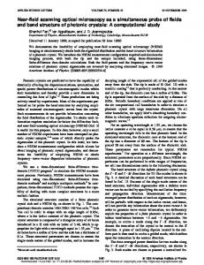
fusion into GaN measured by secondary ion mass spectroscopy 共SIMS兲 and its variation with ECV-measured doping density. The GaN/Al2O3 layers were grown by chloride-transport hydride vapor phase epitaxy 共HVPE兲 from several sources, designated A, B, and C. Source A material incorporated a ZnO buffer layer prior to GaN growth, but the others did not. A modified JEOL 7800F SEM Auger microprobe 共base pressure 8⫻10⫺11 Torr兲 fitted with an Oxford Scientific Mono CL monochromator, a liquid He cold stage, and a visible-UV sensitive photomultiplier tube provided CL spectra. We produced cross sections by scoring the sapphire and cleaving between glass cover slips. CL spectra were obtained using 5 keV electron beam energy 共total penetration depth ⬃160 nm parallel to the interface兲 and 1 nA current over a 0.5 ⫻0.5 m2 raster square area. The inset to Fig. 1 displays a typical room temperature log CL spectrum for a HVPE GaN/Al2O3 interface 共specimen A1兲 with n int⫽8⫻1014 e/cm2, showing peak features at 3.8, 3.42, 2.9, and 2.2 eV. 共Note that the 1.7 and 1.9 eV lines are just second-order transitions.兲 The 3.42 and 2.2 eV features correspond to well-known emissions of the GaN near band edge 共NBE兲 and yellow luminescence 共YL兲, respectively. The NBE, YL, 3.8, and 2.95 eV 共‘‘blue’’兲 peaks exhibit Gaussian line shapes in linear spectra at the energies shown. Their relative peak intensities appear for a similar specimen 共A2, n int⫽5.9⫻1014 e/cm2兲 as a function of raster center distance d int from the interface in Fig. 1. The GaN NBE emission increases rapidly within the first 10 m from the interface into the GaN bulk, then gradually over the next 60 m. The YL emission shows a more gradual increase with d int over the same depth range. Significantly, the absolute YL intensity and its value normalized to the GaN NBE intensity both increase while dislocation density decreases with increasing d int⬎10 m. This result suggests that dislocations are not the source of YL in the ‘‘bulk’’ region.6 The low YL
0003-6951/2001/78(23)/3630/3/$18.00 3630 © 2001 American Institute of Physics Downloaded 21 May 2002 to 164.107.162.113. Redistribution subject to AIP license or copyright, see http://ojps.aip.org/aplo/aplcr.jsp
Appl. Phys. Lett., Vol. 78, No. 23, 4 June 2001
Goss et al.
3631
FIG. 1. CL intensities vs d int of peak features at 3.42 共GaN NBE兲, 2.2 共YL兲, 2.9 共blue兲, and 3.8 eV and 共panel兲 a representative CL spectrum of the HVPE GaN/Al2O3 interface.
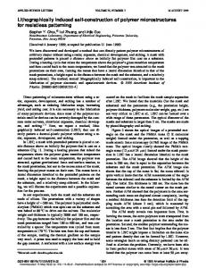
intensity for d int⬍2 m may be due to competing recombination pathways, e.g., via impurity levels. Cr emission at 1.78 eV 共not shown兲 from the Al2O3 decreases rapidly within this d int⬍10 m. The 3.8 eV peak has low intensity within the Al2O3, increases with interface proximity, then disappears in the GaN. It can be due to Al–N–O complexes, since 3.8 eV emission in AlN has been assigned to O impurities,7 and nitridation of Al2O3 forms an amorphous AlNx O1⫺x layer.8 The broad 2.9 eV blue emission intensity is negligible within the Al2O3 or the bulk GaN but is observed for d int ⬍0.2 m. Unlike the 2.9 eV emission commonly reported for heavily Mg-doped p-type GaN, ours is in a n-type sample. Pankove et al.9 have reported broad 2.9 eV CL emission for Zn-doped GaN. Interfacial Zn might be plausible since Source A employed a ZnO buffer on the Al2O3. Such a treatment can result in a Zn-spinel structure10 and residual Zn impurities near the interface. However, the ZnO was thermally desorbed prior to growth, and in any case, sources B and C did not use such a treatment. In order to further elucidate the near-interface donor, we have carried out low temperature 共10 K兲 CLS as a function of d int . The CL spectra in Fig. 2 共specimen B, n int⫽5.0 ⫻1015 e/cm2兲 exhibit typical sharp features in GaN, i.e., shallow-donor-bound exciton (D 0 X) transitions at 3.473 eV and donor-acceptor-pair 共DAP兲 transitions at 3.2–3.3 eV, followed by a sequence of longitudinal optical phonon replicas (⌬h ⫽92– 93 meV). The dominant acceptor may either be C,11 detected by SIMS in similar samples,12,13 or the Ga vacancy, detected by positron annihilation.13 However, it is not likely Mg, which was not detected by SIMS.13 These features are common to GaN at all depths. At d int⭐1 m, an additional feature appears at 3.447 eV, somewhat broader than the 3.473 eV peak. A broad structure is not unexpected in
FIG. 2. Low temperature CL spectra of sample B showing added 3.447 eV shoulder features near the interface.
this highly degenerate region, due to band tailing and band filling 共Moss–Burstein兲 effects. The appearance of both sharp and broad features may be due to inhomogeneity parallel to the interface plane reported previously in similar material.14 Thus, the 3.447 eV line may represent highconcentration regions which are downshifted from the 3.473 eV peak because of band tailing. The 3.449 eV peak may also be a two-electron replica of the 3.473 eV line,15 because such a line would be expected at 3.473 eV⫺(3/4)E D , where E D should be about 34 meV. That is, the final state of the 3.473 eV transition is the ground state (n⫽1) of the donor, whereas the 3.447 eV transition would then have an n⫽2 final state. But if this latter model were correct, then the two transitions might be expected to have about the same line width, which is not the case. The only donor with a high enough concentration to give the observed line broadening of the 3.447 eV line is O, because O increases strongly near the interface, whereas the other major candidate, Si, does not.13 SIMS 关O兴 concentrations characteristic of the 关O兴 diffusion appear in Fig. 2. No other donor impurity is localized in this depth range. Hence, the intensity versus depth distribution indicates that O impurities diffused from the Al2O3 are the origin of the high sheet carrier concentration. Another possibility for the 3.447 eV transition is an exciton bound to a deep donor or acceptor. If the Haynes factor is 0.1–0.2, then this deep center would have an energy of about 150–300 meV from a band edge. An acceptor-bound exciton would be the most likely candidate, since acceptor centers are clearly evident from the strong DAP transitions. Of all possible acceptors, only the Ga vacancy would have a high enough concentration to produce such a broad line.
Downloaded 21 May 2002 to 164.107.162.113. Redistribution subject to AIP license or copyright, see http://ojps.aip.org/aplo/aplcr.jsp
3632
Goss et al.
Appl. Phys. Lett., Vol. 78, No. 23, 4 June 2001
lines near the interfaces of HVPE GaN layers grown on sapphire, evidently due to lateral inhomogeneity in the interface regions. The sharp lines are donor-bound excitons, strongly associated with O shallow donors in the relatively good material, while the broad lines may either be donor-bound excitons in the more highly-concentrated material, or acceptorbound excitons associated with the Ga vacancy. In either case, these spatial correlations between electronic and chemical impurity distributions confirm the high concentrations of diffusion-induced dopants at the GaN/Al2O3 interface. This work is supported by the Office of Naval Research, the National Science Foundation, the Air Force Office of Scientific Research, and the Department of Energy 共depthdependent measurements兲. The authors thank Drs. T. Paskova 共Linko¨ping University兲 and R. Vaudo 共ATMI兲 for samples, as well as Drs. S. Mitha and S. Novak 共Chas. Evans Associates兲 for SIMS profiles. The Lincoln Laboratory portion of this work was sponsored by the Office of Naval Research under Air Force Contract No. F19628-00-C-0002. Opinions, interpretations, conclusions, and recommendations are those of the authors and not necessarily endorsed by the United States Air Force. 1
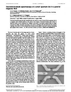
FIG. 3. HVPE GaN/Al2O3 CL near-interface spectra. Band tailing, band filling, and possible alloying, are evident at higher sheet carrier concentration.
However, the YL emission typically associated with Ga vacancies is measured to be low in this region, again supporting the association of the 3.447 eV transition with high concentrations of the O donor. Figure 3 provides a comparison of 10 K NBE spectra from HVPE GaN/Al2O3 interfaces with different n int . Line broadening is evident in all cases, as expected. However, sources B and C appear to have sharp lines on top of broad lines, as just discussed. We believe this is due to more inhomogeneity in these layers, as borne out by the SIMS and other CL data. For sample C, a broad feature centered at 3.59 eV appears. Unlike the case for impurity band filling, even for impurity concentrations ⬎1020 cm⫺3, 14 this peak is centered well above the conduction band edge and may be due in part to GaN–Al alloying. Such Alx Ga1⫺x N alloying and NBE features are observed at Al–GaN interfaces,16 and Al–N bonding is not unexpected, given the O release from Al2O3 at the atomic–scale interface. Pregrowth nitridation of sapphire for such specimens17 should further enhance Al–N bonding and alloying. In conclusion, we observe both sharp and broad NBE CL
W. Go¨tz, J. Walker, L. T. Romano, N. M. Johnson, and R. J. Molnar, Mater. Res. Soc. Symp. Proc. 449, 525 共1997兲. 2 D. C. Look and R. J. Molnar, Appl. Phys. Lett. 70, 3377 共1997兲. 3 X. L. Xu, C. D. Beling, S. Fung, Y. W. Zhao, N. F. Sun, T. N. Sun, Q. L. Zhang, H. H. Zhan, B. Q. Sun, J. N. Wang, W. K. Ge, and P. C. Wong, Appl. Phys. Lett. 76, 152 共2000兲. 4 G. Popovici, W. Kim, A. Botchkarev, H. Tang, H. Morkoc, and J. Solomon, Appl. Phys. Lett. 71, 3385 共1997兲. 5 J. E. Van Nostrand, J. Solomon, A. Saxler, Q.-H. Xie, D. C. Reynolds, and D. C. Look, J. Appl. Phys. 87, 8766 共2000兲. 6 M. Godlewski, E. M. Goldys, M. R. Phillips, R. Langer, and A. Barski, Appl. Phys. Lett. 73, 3686 共1998兲. 7 R. A. Youngman and J. H. Harris, J. Am. Ceram. Soc. 73, 3238 共1990兲. 8 K. Uchida, A. Watanabe, F. Yano, M. Kouguchi, T. Tanaka, and S. Minagawa, J. Appl. Phys. 79, 3487 共1996兲. 9 J. I. Pankove and J. A. Hutchby, J. Appl. Phys. 47, 5387 共1976兲. 10 S. Gu, R. Zhang, J. Sun, L. Zhang, and T. F. Kuech, Appl. Phys. Lett. 76, 3454 共2000兲. 11 B. K. Meyer, D. Volm, A. Graber, H. C. Alt, T. Detchprohm, A. Amano, and I. Akasaki, Solid State Commun. 95, 597 共1995兲. 12 Chas. Evans and Associates, 810 Kaifer Rd., Sunnyvale, California. 13 D. C. Look, C. E. Stutz, R. J. Molnar, K. Saarinen, and Z. Liliental-Weber, Solid State Commun. 117, 571 共2001兲. 14 B. Arnaudov, T. Paskova, E. M. Goldys, R. Yakimova, S. Evtimova, I. G. Ivanov, A. Henry, and B. Monemar, J. Appl. Phys. 85, 7888 共1999兲. 15 M. Leroux, N. Grandjean, B. Beaumont, G. Nataf, F. Semond, J. Massies, and P. Gibart, J. Appl. Phys. 86, 3721 共1999兲. 16 A. P. Young, J. Schafer, L. J. Brillson, Y. Yang, S. H. Xu, H. Cruguel, G. J. Lapeyre, M. A. L. Johnson, and J. F. Schetzina, J. Electron. Mater. 28, 308 共1999兲. 17 N. Grandjean, J. Massies, and M. Leroux, Appl. Phys. Lett. 69, 2071 共1996兲.
Downloaded 21 May 2002 to 164.107.162.113. Redistribution subject to AIP license or copyright, see http://ojps.aip.org/aplo/aplcr.jsp