APPLIED PHYSICS LETTERS
VOLUME 75, NUMBER 16
18 OCTOBER 1999
Infrared and photoluminescence spectroscopy of p -doped self-assembled Ge dots on Si L. P. Rokhinsona) and D. C. Tsui Department of Electrical Engineering, Princeton University, Princeton, New Jersey 08544
J. L. Benton and Y.-H. Xieb) Bell Laboratories, Lucent Technologies, Murray Hill, New Jersey 07974
共Received 14 June 1999; accepted for publication 17 August 1999兲 We report infrared photocurrent 共PC兲 and photoluminescence 共PL兲 spectroscopy of self-assembled Ge dots grown on Si共100兲 by molecular beam epitaxy. PL spectra show a transition from two- to three-dimensional growth as the Ge thickness exceeds 7 Å. The sum of the PC peak energy and PL energy from Ge dots is found to be approximately equal to the energy band gap of Si. Boron doping changes the energy spectrum of the dots: PL peaks from both doped Ge dots and from the wetting layer are shifted to higher energy, compared to the undoped samples. Also, the TO phonon energy from the wetting layer is reduced to 38 meV. © 1999 American Institute of Physics. 关S0003-6951共99兲00442-8兴
Quantum well infrared photodetector 共QWIP兲 technology has matured rapidly in the last several years.1 As a result, GaAs/AlGaAs QWIPs are used nowadays in a variety of applications, ranging from military applications to remote temperature sensing. To enable an even wider use of QWIPs compatibility with silicon-based technology is highly desired. Attempts have been made to fabricate QWIPs on SiGe/Si heterostructures utilizing intersubband transitions in the valence band of multiple quantum well 共MQW兲 structures.2–5 However, pseudomorphic growth of Ge on Si has been limited by the critical thickness, d cr , due to the 4% lattice mismatch; and for larger Ge coverage, stress has been released through dislocations. Recently, it was found that, under certain conditions, stress is released through the formation of dislocation-free Ge-rich dots on Si surface 共Stranski-Krastanov type of growth兲. In this mode, the total amount of Ge is not limited to d cr , and multiple layers can be grown. An ability to grow a large number of layers with self alignment of dots in the vertical direction6 is the prerequisite for optical applications, such as infrared photodetection. Structural studies show that for Ge coverage ⬍7 Å twodimensional strained quantum wells 共QWs兲 are grown 共2D mode兲, while for higher amount of Ge, a sharp transition to three-dimensional growth 共3D mode兲 is observed.7–9 In 3D mode, Ge-rich dots of average diameter 1000 Å and thickness 100 Å are formed on top of a strained Ge wetting layer 共WL兲 which is 1–2 monolayers thick. During growth, the underlying Ge dots become preferential nucleation sites for the formation of dots in the subsequent layers, thus resulting in the self alignment of dots in the growth direction. Photoluminescence studies of self-assembled Ge dots have provided an easy way to identify the transition from 2D to 3D growth and have provided some insight about the band structure.7,8,10,11 Infrared spectroscopy is a direct way to
measure band alignment, which should be known in order to design devices on intersubband transitions. For practical photodetector applications, high doping is essential. We found that doping results in an unexpected shift of the energy levels in these structures. We present a combined photoluminescence and photoconductance study of doped and undoped self-assembled Ge dots. We report, for the first time, a realization of an infrared photodetector with low-energy cutoff wavelength of ⬇11 m on self-assembled Ge dots in Si. Wafers were grown by molecular beam epitaxy 共MBE兲 on Si共001兲 substrates. The growth temperature was kept at 700 °C. Each wafer consists of 10 Ge layers separated by 200 Å of Si. The thickness of the Ge layers was varied from 2 to 10 Å. The wafer with 7 Å of Ge were boron doped in the Ge layers. For in-plane photocurrent measurements aluminum contacts were alloyed at 400 °C for 2 min. Photocurrent was measured at 5 K in a prism far infrared spectrometer using an alternating-current 共ac兲 lock-in technique. Measurements were done in either two-terminal photocurrent or fourterminal photoresistance configuration; both methods showed similar results. To confirm that the doping was confined to the Ge dots, we studied the temperature dependence of the lateral resistivity, Fig. 1. At high temperatures 40 K⬍T⬍70 K, carrier transport is thermally activated, while at T⬍25 K, the temperature dependence of resistivity is consistent with variable range hopping,12 ⬀exp(T1 /T)1/2, where k B T 1 ⫽2.8e 2 / ⑀⑀ 0 . The estimated localization length is ⬇1000 Å, which is approximately the lateral size of the Ge dots. This result provides evidence that the holes are localized within Ge dots. A series of PL spectra from samples with increasing Ge coverage are shown in Fig. 2. The pair of peaks at high energies is attributed to no-phonon 共NP兲 and TO-phonon assisted PL from the Ge-rich narrow wetting layer 共WL兲. The appearance of broad peaks at lower energies 共labeled ‘‘dots’’兲 coincides with the onset of Ge dot formation and was earlier attributed to electron-hole recombination within
a兲
Electronic mail:
[email protected] Current address: Department of Material Science and Engineering, UCLA, Los Angeles, CA 90095.
b兲
0003-6951/99/75(16)/2413/3/$15.00
2413
© 1999 American Institute of Physics
2414
Appl. Phys. Lett., Vol. 75, No. 16, 18 October 1999
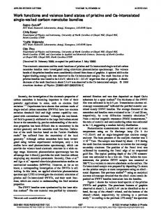
FIG. 1. Temperature dependence of the resistivity for the doped sample with 7 Å Ge. The top inset shows that low temperature conduction is well described by the variable range hopping ( ⬀exp关(T1 /T)1/2兴 ). At higher temperatures the transport is temperature activated with activation energy ⬇36 meV.
the dots or at the interface between the dots and surrounding Si.8 These peaks can be decomposed into two Lorentzianshaped peaks which correspond to NP- and TO-phonon assisted recombination 共thin lines in Fig. 2兲. The energy of the NP peak versus Ge coverage are plotted in Fig. 3. NP peak energies for undoped samples are in excellent agreement with the data reported by Abstreiter et al.8 However, for samples from doped wafers 共with 7 Å Ge兲, energies of the
FIG. 2. Photoluminescence spectra for samples with different Ge coverage were measured at 3 K with excitation power 480 mW. Positions of Si TO, TA phonon replicas and bound exciton 共BE兲 are shown. Peaks labeled ‘‘WL’’ originate from wetting layers while peaks labeled ‘‘dots’’ are attributed to PL from Ge dots. Dashed lines are Lorentzian fits to the peaks. The energy difference between the NP and TO peaks from the WL are indicated.
Rokhinson et al.
FIG. 3. PL energy of the no-phonon transitions in the wetting layer 共squares兲 and in the Ge dots 共triangles兲 are plotted as a function of Ge coverage. Solid symbols are data from our samples; samples with 2, 3, 5, and 10 Å of Ge are undoped and the sample with 7 Å of Ge is p doped. Data reported by Schittenhelm et al. 共Ref. 7兲 for undoped structures 共open symbols兲 are shown for comparison. Dashed lines are guides for the eye.
NP peaks from both the WL and the Ge dots are higher than reported for undoped samples with the same Ge coverage. It is commonly accepted that Ge dots in Si have type II band alignment with most of the band offset being taken up in the valence band discontinuity. It was shown13 that in Si1⫺x Gex /Si quantum wells even at moderate excitation levels band bending, produced by type II charge separation, changes the conduction band alignment to type I and moves electrons into the Si1⫺x Gex region. In either case we expect that optical transitions involve electrons close to the Si conduction band edge Ec (Si) 共see inset in Fig. 4兲. However, interpretation of the photoluminescence data is not unambiguous: in indirect gap materials NP photoluminescence requires some scattering mechanism to relax momentum conservation, such as random alloy scattering or scattering on dislocations at the dot–Si interface. Due to diffusion, Ge content near the edge of the dot could be lower than in the dot center, resulting in smaller valence band discontinuity. Consequently, if the NP peak in the PL is due to radiative recombination at the dot–Si interface, the measured NP peak energy can be larger than the band gap in the center of the dot. Since we do not know a priori where recombination occurs, the photoluminescence data alone is not sufficient to infer the valence band offset in the center of the Ge dot. In contrast, infrared spectroscopy directly probes the ground state in the dot. In p-type SiGe coupling between heavy-hole, light-hole, and spin-orbit split-off bands relaxes the dipole selection rule and intersubband transitions are allowed for all light polarizations. Photocurrent response 共PC兲 for the sample with 7 Å Ge is plotted in Fig. 4. The light was incident perpendicular to the surface and current was measured in the plane perpendicular to the growth direction. The photocurrent reaches its maximum at 200 meV which we attribute to the hole excitation from the ground state in the Ge dot to the Si valence band E v (Si) 共see inset in Fig. 4兲.
Rokhinson et al.
Appl. Phys. Lett., Vol. 75, No. 16, 18 October 1999
FIG. 4. Photocurrent in the sample with 7 Å Ge coverage measured at 5 K. The dip at 140 meV is due to SiO2 absorption. Inset shows schematically the band diagram of the wetting layer and the Ge dot sandwiched between Si layers. PL transitions are shown by dashed arrows. At low temperatures holes are localized within the Ge dots. Extended states for hole transport are in the Ge wetting layer and in the Si valence band; corresponding infrared transitions are shown by solid arrows. Note, that Ge dots and the wetting layer are not spacially separated.
The onset of the photocurrent is expected for the hole excitation from the ground state in the dot into the ground state in the wetting layer. Comparison of PL and PC spectra shows that the energy difference between the NP peaks from the dots and from the wetting layer 共123 meV兲 is close to the onset of the photocurrent (⬇110 meV), and that the sum of the energy of the NP peak from the dots 共995 meV兲 and the energy of photocurrent maximum (⬇200 meV) is approximately equal to the band gap of Si at 4 K 共1170 meV兲. In the latter case, some small discrepancy is expected because we neglected the difference in the binding energies of the exciton in the dots and the WL, the nonzero Fermi energy, and the finite broadening of spectra due to the nonuniformity of the dots. From the above comparison we conclude that both photoluminescence and infrared spectroscopy probe the energy of the ground state in the dot. Since we have established that the NP dot peak corresponds to the hole ground state in the dot, there are only two possibilities for the shift of the NP peaks in the doped samples: stronger quantum confinement due to smaller dot size and narrower WL, or a change in the valence band offset due to different Ge composition and/or stress distribution. However, the effect of doping leads to a decrease of the band gap14 which is opposite to our observations. The height, ⬇100 Å, and diameter, ⬇1000 Å, of the dots in our samples, obtained from transmission electron microscopy 共TEM兲 images, are similar to the ones studied by Abstreiter et al.;8 and the small difference in size cannot explain the approximately ⬇100 meV increase in NP energy. In a recent
2415
letter, Bottomley15 proposed that stress-induced lowering of the melting point in SiGe heterostructures might lead to the mixture of Ge with the Si substrate. The critical strain for the melting of Ge grown on Si at 700C is only ⫺0.7%, which corresponds to the strain in Si0.83Ge0.17 pseudomorphically grown on Si. The minimum Gibbs free energy is predicted for an alloy with ⬇50% of Ge. Thus, we expect the composition of the dots to be sensitive to the growth conditions, including the presence of doping. In undoped samples, the WL-related pair of peaks is separated by 58 meV which corresponds to the Si-Si TO phonon energy, Fig. 2. Phonons are three-dimensional and are not confined to the Ge layer. In contrast, in doped samples, the separation between these peaks is only 38 meV, close to the energy of Ge-Ge TO phonon 共36 meV兲, suggesting that phonons are confined within the 2D layer. A similar confinement of acoustic phonons was reported in modulation-doped Ge/Si0.4Ge0.6 quantum wells.16 Note, that in undoped samples with a comparable thickness of Ge layer 共7.2 Å兲, a 58 meV TO phonon energy has been measured.8 In this work, we report an infrared photodetector on Ge self-assembled dots with cutoff energy ⬇110 meV 共11 m兲. We found that introduction of doping reduces the valence band offset between the Ge dots and Si. Presumably, the presence of boron atoms shifts the thermodynamical balance during the growth toward lower-Ge content dots. The work at Princeton University was partially supported by the ARO.
K. K. Choi, The Physics of Quantum Well Infrared Photodetectors 共World Scientific, River Edge, NJ, 1997兲. 2 J. S. Park, R. P. G. Karunasiri, and K. L. Wang, Appl. Phys. Lett. 60, 103 共1992兲. 3 R. People, J. C. Bean, S. K. Sputz, C. G. Bethea, and L. J. Peticolas, Appl. Phys. Lett. 61, 1122 共1992兲. 4 T. Fromherz, E. Koppensteiner, M. Helm, G. Bauer, J. F. Nu¨tzel, and G. Abstreiter, Phys. Rev. B 50, 15073 共1994兲. 5 P. Kruck, M. Helm, T. Fromherz, G. Bauer, J. F. Nu¨tzel, and G. Abstreiter, Appl. Phys. Lett. 69, 3372 共1996兲. 6 P. M. Petroff and S. P. DenBaars, Superlattices Microstruct. 15, 15 共1994兲. 7 P. Schittenhelm, M. Gail, J. Brunner, J. F. Nu¨tzel, and G. Abstreiter, Appl. Phys. Lett. 67, 1292 共1995兲. 8 G. Abstreiter, P. Schittenhelm, C. Engel, E. Silveira, D. Meertens, and W. Ja¨ger, Semicond. Sci. Technol. 11, 1521 共1996兲. 9 E. S. Kim, N. Usami, and Y. Shiraki, Appl. Phys. Lett. 70, 295 共1997兲. 10 H. Sunamura, Y. Shiraki, and S. Fukatsu, Appl. Phys. Lett. 66, 953 共1995兲. 11 R. Apetz, L. Vescan, A. Hertmann, C. Dieker, and H. Lu¨th, Appl. Phys. Lett. 66, 445 共1995兲. 12 B. I. Shklovskii and A. L. Efros, Electronic Properties of Doped Semiconductors 共Springer, New York, 1994兲. 13 M. L. W. Thewalt, D. A. Harrison, C. F. Reinhart, J. A. Wolk, and H. Lafontaine, Phys. Rev. Lett. 79, 269 共1997兲. 14 B. M. Manning, C. J. Peters, N. G. Tarr, J.-P. Noel, and D. C. Houghton, J. Vac. Sci. Technol. B 11, 1190 共1993兲. 15 D. J. Bottomley, Appl. Phys. Lett. 72, 783 共1998兲. 16 S.-H. Song, W. Pan, D. C. Tsui, Y.-H. Xie, and D. Monroe, Appl. Phys. Lett. 70, 3422 共1997兲. 1