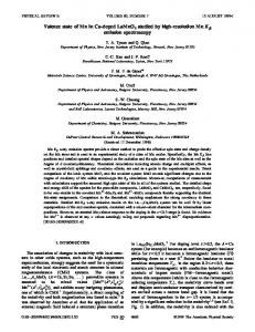
Feb 1, 2001 - Delphi Research Labs, Delphi Automotive Systems, Shelby Township, Michigan 48316. Yu-Ming Lin. Department of Electrical Engineering and ...
PHYSICAL REVIEW B, VOLUME 63, 085406
Transport properties of antimony nanowires J. Heremans and C. M. Thrush Delphi Research Labs, Delphi Automotive Systems, Shelby Township, Michigan 48316
Yu-Ming Lin Department of Electrical Engineering and Computer Science, Massachusetts Institute of Technology, Cambridge, Massachusetts 02139
S. B. Cronin Department of Physics, Massachusetts Institute of Technology, Cambridge, Massachusetts 02139
M. S. Dresselhaus* Department of Physics and Department of Electrical Engineering and Computer Science, Massachusetts Institute of Technology, Cambridge, Massachusetts 02139 ⵥReceived 14 June 2000; revised manuscript received 27 September 2000; published 1 February 2001䊝 This paper reports the temperature dependence of the resistivity and the longitudinal and transverse magnetoresistance of antimony quantum wires with diameters ranging from 200 down to 10 nm. The samples were prepared in porous anodic alumina host materials using the vapor-phase technique. A theoretical calculation of the band structure of Sb nanowires is presented and a transport model for nanowire systems is used to explain the measured temperature dependence of the resistivity, showing both classical and quantum finite-size effects. The magnetoresistance is quadratic at low fields. In the 200 nm wires, the low-temperature (T⬍50 K) longitudinal magnetoresistance exhibits a maximum at the magnetic field where the cyclotron radius roughly corresponds to the wire radius. Surface scattering dominates below that field, and bulklike scattering dominates above it. In the narrower wires, the low-temperature ⵥbelow 10 K for 50 nm wires and below 40 K for 10 nm wires䊝 magnetoresistance shows a steplike feature at the critical magnetic field where the magnetic length equals the wire diameter, as was the case for bismuth wires. This phenomenon is independent of the effective masses, depending only on the geometry of the nanowires and on the magnetic flux in the wire, and it is therefore attributed to a localization effect. DOI: 10.1103/PhysRevB.63.085406
PACS numberⵥs䊝: 73.40.⫺c
INTRODUCTION
The transport properties of bismuth ⵥBi䊝 thin wires have been investigated extensively for several decades.1–3 A second wave of studies has been more recently initiated as a result of the calculations of Hicks and Dresselhaus,4 who predicted that Bi nanowires should have a thermoelectric figure of merit strongly enhanced over that for bulk Bi, and possibly higher than for conventional thermoelectric materials. Zhang et al.5 synthesized Bi nanowires in porous anodic alumina using a high-pressure liquid injection technique, similar to that in the older work, but using a surfactant to lower the pressure necessary for filling the pores. A vaporphase preparation technique6 was developed to prepare Bi nanowires with diameters down to 7 nm. Both preparation techniques produce Bi nanowires with a preferential crystallographic orientation: the long axis of the wires aligns with ¯ 1 䊟 or 䊞 011 ¯ 2 䊟 directions in the hexagonal structural the 䊞 101 description ⵥor 䊞 x,y,z 䊟 ⫽ 䊞 0,0.949,0.315䊟 and 䊞0,0.834, 0.552䊟 in Cartesian coordinates, respectively䊝.3,5,6 Exceptions to these two orientations are the Bi wires of Huber et al.,7 which are reported to have a long axis along the trigonal 䊞0001䊟 direction, and the Bi wires prepared by electrochemical means,8 which are polycrystalline. The galvanomagnetic,6,9,10 thermoelectric,11,12 and thermal13 ¯ 1 䊟 -oriented Bi nanowire arrays have properties of the 䊞 101 been extensively reported. In the present paper, we extend this work to nanowire 0163-1829/2001/63ⵥ8䊝/085406ⵥ8䊝/$15.00
arrays of another group-V semimetal: antimony ⵥSb䊝. As in Bi, electronic transport phenomena in Sb occur via both electrons and holes. The energy overlap between the conduction and valence bands is about 180 meV at 4.2 K.14,15 The electrons are located, as in Bi, in three ellipsoidal carrier pockets centered at the L points of the Brillouin zone. Each electron Fermi ellipsoid14 has a long axis tilting by about ⫺4° from the bisectrix axis. The effective-mass components of the electron ellipsoids in Sb are much larger than those in Bi. The hole Fermi surface of Sb is quite complex, but can be approximated by two sets of three prolate ellipsoids at the equivalent H points of the Brillouin zone,15 with the principal axes of the three ellipsoids in each set pointing to a T point of the Brillouin zone. The longest and shortest axes of the hole ellipsoids are in the trigonal-bisectrix plane, with the intermediate axis oriented along the binary axis. The angle between their longest axis and the trigonal axis is about 53°. The effective-mass components of the hole ellipsoids of Sb are of the same order of magnitude as those in Bi. The Sb wire arrays were prepared in porous anodic alumina templates using the vapor-phase deposition technique,6 similar to those used for our previous Bi work. Here we report the temperature dependence of the resistance, and the magnetic-field dependence of the longitudinal and transverse magnetoresistance. A theoretical calculation of the band structure of Sb nanowires is presented, using a model for anisotropic carriers confined to an infinite cylindrical wire.16 A semiclassical transport model for nanowire systems10 is
63 085406-1
©2001 The American Physical Society
HEREMANS, THRUSH, LIN, CRONIN, AND DRESSELHAUS
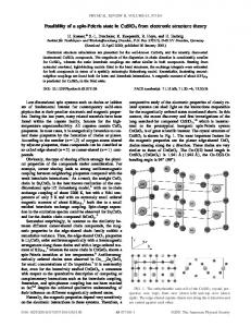
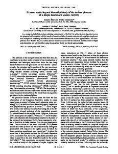
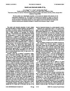
FIG. 1. X-ray diffraction signal vs scattering angle 2ⵧ of the 200 nm diameter Sb wire array. The vertical lines are the reported peak positions for polycrystalline Sb. The inset shows the sample geometry.
used to explain the measured temperature-dependent resistance for Sb nanowire arrays. The experimental data for the magnetoresistance measurements are interpreted qualitatively by analogy with those for Bi nanowire arrays. SAMPLE PREPARATION AND EXPERIMENT
Porous anodic alumina templates6 were used as host materials for the fabrication of Sb nanowire arrays. Briefly, porous alumina was produced by anodizing pure aluminum films in 20 wt % sulfuric acid, resulting in an array of hexagonally packed pores. Prior to the vapor deposition, the residual aluminum film and the barrier layer are etched away by 0.2M HgCl2 and 5 wt % H3PO4, respectively, leaving a free-standing alumina template with pores that are open on both sides. The removal of the barrier layer is essential for the following vapor deposition of Sb nanowires and subsequent transport measurements. The pore diameters of the samples used in this work are d W ⫽200, 48⫾6, and 10 ⫾2 nm, with an average interpore distance of 400, 116⫾6, and 50 nm, respectively. The pores were filled with Sb using the same vapor-phase filling apparatus as described in Ref. 6, but with a higher operating temperature. No special care was used during the sample cool-down. An x-ray diffraction spectrum of the 200 nm wire sample is shown in Fig. 1, along with the diffraction peaks for a polycrystalline Sb standard. The inset shows the schematic diagram of the sample setup. Since no peaks are observed in our sample, we conclude that the Sb nanowires are either amorphous or consist of a very fine-grained polycrystalline material. The resistance and magnetoresistance data were taken on arrays of Sb nanowires using a two-contact technique,9 with
PHYSICAL REVIEW B 63 085406
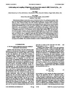
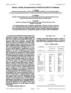
FIG. 2. Experimental temperature dependence of the resistance of Sb nanowires of various diameters, normalized to the resistance at 300 K.
electrical current flowing parallel to the wire axis. The discussion on contact resistance issues reported in Refs. 6 and 9 also holds here. In particular, two samples of each diameter were measured and the results were found to be reproducible, unless otherwise indicated. The samples were placed inside a variable-temperature inset in a 5 T superconducting magnet, and the resistances were measured by a low-frequency ac impedance bridge ⵥLinear Instruments LR-700䊝. The results are independent of excitation voltage, which was varied from 2 to 600 䉱V. Resistance data were taken from 1.4 to 300 K, while results of the magnetoresistance are reported only from 1.4 to 70 K because the magnet cannot be activated above 80 K. Both the longitudinal magnetoresistance ⵥmagnetic field B parallel to current䊝 and the transverse magnetoresistance ⵥB normal to current䊝 were measured. ZERO-FIELD TEMPERATURE-DEPENDENT RESISTANCE Experimental results
Figure 2 shows the temperature dependence of the resistance of the Sb nanowires, normalized to the resistance at 300 K, in the absence of a magnetic field. The results for the larger-diameter wires are reproducible from sample to sample. One sample of the 10 nm wire shows less temperature variation that the other, probably due to a different distribution in wire diameter or in impurity content. The R(T) of Sb nanowires exhibits a rather different trend from those for Bi nanowires as the wire diameter varies. Contrasting Fig. 2 with Fig. 3 of Ref. 6, one notices that the clear signature of the semimetal-to-semiconductor transition observed in Bi nanowires6 is absent in Sb nanowires for the measured diameter range. For Bi nanowires with diameters d W ranging
085406-2
TRANSPORT PROPERTIES OF ANTIMONY NANOWIRES
PHYSICAL REVIEW B 63 085406
TABLE I. Calculated subband structure parameters for Sb nanowires oriented along the three major axes. The parameters ˜« h and ˜« e ⵥin units of meV nm2䊝 and m ˜* e ⵥin units of the free-electron mass䊝 can be used in Eqs. ⵥ3䊝 and ⵥ4䊝 to derive the first-subband-edge energies and the transport effective masses of the charge carriers. The hole transport mass m * h is also given in units of the free-electron mass. Bisectrix Orientation ˜« h m h* ˜« e m ˜* e
Trigonal
Group I
Group II
Group I
Group II
9.70⫻103 0.340 1.08⫻104 0.043
1.25⫻104 0.630 2.13⫻104 0.525
9.88⫻103 0.209 1.41⫻104 0.163
8.78⫻103 0.068 1.14⫻104 0.043
1.17⫻104 0.490 1.89⫻104 0.404
from 10 to 200 nm, the measured resistance changes from a monotonic T dependence to a nonmonotonic dependence as d W increases, while R(T) of Sb nanowire arrays in this range of d W exhibits less variation in T. Qualitatively, the gross features of Fig. 2 can be explained in terms of the relative importance of electron-phonon scattering, which increases with temperature, and electron-boundary scattering, which is relatively T independent. Since the Sb nanowires are expected to remain metallic for the measured diameter range ⵥas will be shown later䊝, the carrier density is a weak function of T, and the R(T) is mainly determined by the T dependence of the various scattering mechanisms. At high temperatures (T⬎100 K), the phonon scattering dominates and the resistance rises with increasing T. As the temperature is lowered, the boundary scattering becomes dominant, giving rise to a less T-dependent resistance for T⬍100 K, which explains the general features of the measure R(T) for the various Sb nanowire arrays shown in Fig. 2. As the wire diameter decreases, the boundary scattering becomes relatively more important than for larger-diameter wires, since a larger portion of the carriers are located near the wire boundary. Therefore, smaller-diameter wires exhibit less temperature variation than larger-diameter wires. Theoretical modeling
In order to quantitatively explain the experimental results in Fig. 2, a semiclassical transport model for the Sb nanowires is developed, based on the detailed band structure of Sb nanowires. The band structure of Sb nanowires is derived from a model developed recently for Bi nanowire systems to determine the subband structure of anisotropic carriers confined within a cylindrical wire of infinite length.16 In addition, due to the coupling between the holes and electrons at the L points of the Brillouin zone of Sb, the following nonparabolic dispersion relation is used for the L-point carriers:14 E L ⵥ k䊝 ⫽⫺
Binary
Eg J •k, ⫾ 冑E 2g ⫹2E g ⱔ 2 k• 义 2
ⵥ1䊝
where E g ⬜100 meV is the direct band gap at the L point17 and 义 J is the inverse effective-mass tensor at the band edge. The subbands formed by carriers confined in an infinite cylindrical quantum wire, with the wire axis denoted by the z direction, have an E(k) dispersion relation of the form16
E nm ⵥ k z 䊝 ⫽« nm ⫹
ⱔ 2 k z2 2m z*
,
ⵥ2䊝
where « nm is the band-edge energy of the (n,m) subband calculated to include nonparabolic effects, and m z* ⫽zˆ • 义 J ⫺1 •zˆ is the transport effective mass along the wire 16 axis. Since the dispersion energy is small, a parabolic approximation is sufficient to describe the k z dependence. Using the band structure parameters of bulk Sb, the energy shifts of the first subband edges of each electron and hole pocket with respect to the corresponding band edges in bulk Sb are given by16 DE ⵥ d W 䊝 ⫽
再
2 ⫺« ˜ h /d W
ⵥmeV䊝
for holes
2 ⫺E g ⫹ 冑E 2g ⫹4« ˜ e E g /d W
ⵥmeV䊝
for electrons, ⵥ3䊝
where d W is the wire diameter in nanometers, and ˜« e and ˜« h are parameters calculated numerically using the cylindrical boundary conditions. It is noted that due to the anisotropic carriers in Sb the subband-edge energies « nm and the transport effective mass m z* are both highly dependent on the wire orientation. Values for the calculated ˜« e , ˜« h , and transport effective masses m z* are given in Table I for Sb nanowires oriented along the three major axes. As in Bi, the transport effective mass m z* of the L-point carriers in Sb is a function of the subband-edge energy « nm due to the nonparabolicity.16 The effective masses of these nonparabolic carriers are then determined by the curvature of the dispersion relation at the subband edge, which is given by16 m z* ⫽ 冑1⫹4« ˜ nm /E g •m ˜ z* ,
ⵥ4䊝
˜ z* are the values given in Table I. We note that, for where m trigonal Sb wires, the three electron pockets and the six hole pockets are degenerate. However, for wires oriented along the binary and bisectrix directions, the carrier pockets are divided into two groups, based on symmetry considerations. The carrier pockets with their major axes lying in the plane spanned by the wire axis and the trigonal axis for bisectrix wires or in the plane perpendicular to the wire axis for binary wires are denoted as group I, while other pockets that possess different symmetries are denoted as group II. Therefore,
085406-3
HEREMANS, THRUSH, LIN, CRONIN, AND DRESSELHAUS
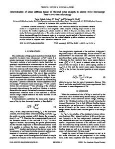
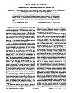
FIG. 3. Calculated band overlap between the electrons and holes as a function of wire diameter for the three major crystalline orientations of the Sb nanowires. The critical wire diameters at which the band overlap vanishes are about 9 nm.
for binary and bisectrix wires, the two groups of pockets form two sets of subbands with different transport effective masses along the wire axis ⵥsee Table I䊝. Due to quantum confinement effects, the subband edges of the electrons and holes shift in opposite directions, decreasing the band overlap between the L-point conduction and the H-point valence bands. As d W continues to decrease, the band overlap will eventually vanish, leading to a semimetal-semiconductor transition in Sb nanowires. Figure 3 shows the calculated band overlap for Sb nanowires as a function of d W for the three major crystalline orientations along the nanowire axis. The critical wire diameters d c for the semimetal-semiconductor transition at which the band overlap is predicted to vanish are 9.6, 10.0, and 9.3 nm for Sb wire axes oriented along the trigonal, bisectrix, and binary directions, respectively. These calculation show that the critical wire diameters d c are much smaller than those of Bi nanowires, which are predicted to be between 40 and 55 nm at 77 K,16 depending on the wire orientation. These smaller values for the critical wire diameter are consistent with the much larger band overlap and higher carrier effective masses of Sb relative to Bi. Since the samples used here did not show any preferred crystallographic orientation ⵥsee Fig. 1䊝 and the band parameters of Sb wires are not very different from each other for wires oriented along the three major orientations ⵥsee Fig. 3䊝, we choose the trigonal wire orientation, as an example, for the following transport modeling. Figure 4 shows the calculated total carrier density in Sb nanowires for various wire diameters. We note that the carrier densities in Sb nanowires are lower than those of bulk Sb and the carrier densities decrease as d W decreases, because of a smaller band overlap for narrower wires. However, the temperature dependence of the carrier density for Sb wires did not change significantly as the wire diameter was varied down to 10 nm, in contrast to that of Bi nanowires, which shows a strong diameter dependence in this diameter range.16 This different behavior is
PHYSICAL REVIEW B 63 085406
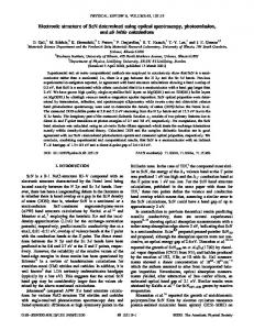
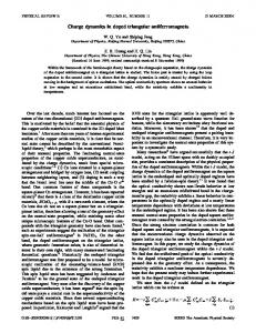
FIG. 4. Calculated total carrier density as a function of temperature for Sb nanowires with various diameters, compared to that of bulk antimony.
due to a less T-dependent band structure and a much larger band overlap in bulk Sb as compared to Bi. The carrier density of 10 nm Sb wires exhibits a slightly stronger T dependence than other larger-diameter wires in Fig. 4, since 10 nm is close to the critical wire diameter for the semimetalsemiconductor transition. Figure 5 shows the calculated R(T) for 10 and 48 nm trigonal Sb nanowire arrays, displaying trends qualitatively consistent with the experimental results shown in Fig. 2. In the semiclassical transport model, the conductivity of the one-dimensional ⵥ1D䊝 systems is derived by16 pockets subbands
䊊⫽
䉺i 䉺 n,m
4e 䉱 i m ⵥ*i,n,m 䊝 2 ⴱ 2d W
冕 冉
dk ⫺
冊
df vⵥ k 䊝vⵥ k 䊝 , dE ⵥ5䊝
FIG. 5. Calculated temperature dependence of the resistance for 48 and 10 nm Sb nanowires, normalized to the resistance at 300 K.
085406-4
TRANSPORT PROPERTIES OF ANTIMONY NANOWIRES
PHYSICAL REVIEW B 63 085406
* where m (i,n,m) is the transport effective mass of the (n,m) subband in the ith pocket, 䉱 i is the carrier mobility, v is the carrier group velocity, and f (E) is the Fermi-Dirac distribution function. In addition to the dominant electron-phonon scattering in bulk Sb, the expected carrier scattering at the wire boundary and at grain boundaries in nanowires is taken into consideration by Matthiesen’s rule:18 ⫺1 ⫺1 ⫺1 䉱 tot,i ⫽ 䉱 bulk,i ⫹ 䉱 bound ,
ⵥ6䊝
where 䉱 bulk,i is the carrier mobility of the ith pocket along ⫺1 is the contrithe wire axis in bulk crystalline Sb, and 䉱 bound bution to the total scattering rate from boundary scattering. Since the mobility of each carrier pocket in Sb is anisotropic, ⫺1 we have 䉱 bulk,i ⫽zˆ • 䉱 J ⫺1 ˆ , where 䉱 J i is the mobility tensor i •z of the ith carrier pocket. The mobility tensor components of 䉱 J i are highly temperature dependent, and empirical relations from the literature19 for single-crystal Sb are used here. On the other hand, the band structure parameters of Sb, unlike Bi, are relatively temperature independent20 for 4⬍T ⬍300 K, and are assumed to be constant in the calculations. The curve of R(T) normalized to the room-temperature resistance for the 10-nm Sb nanowire arrays in Fig. 5 is fitted by 䉱 bound⫽6.67⫻10⫺2 m2 /V s and the carrier density contribution due to the uncontrolled impurities is fitted by N imp ⫽4⫻1018 cm⫺3. The data for the 48-nm Sb nanowires are fitted by 䉱 bound⫽1.0⫻10⫺1 m2 /V s. Since 48-nm Sb nanowires are still semimetallic with a large band overlap ⵥ⬊168 meV䊝, the carrier density contribution due to N imp can be neglected. We note that the 䉱 bound calculated here is about two orders of magnitude smaller than for the case of highly crystalline Bi nanowires ( 䉱 bound⫽33 m2 /V s for 36-nm Bi nanowire arrays䊝.10 Since the Sb nanowires used here are polycrystalline with many grain boundaries, 䉱 bound is expected to be more dominant and to have a lower value than in single-crystal wires. In addition, the larger carrier effective masses in Sb may also contribute to the lower value of 䉱 bound . The fact that the measured R(T) of Sb and Bi nanowires can be explained by the same transport model suggests that the different temperature dependence of the resistance in nanowires from that of the bulk materials is a consequence of both quantum and classical finite-size effects. The classical finite-size effect decreases the carrier mobility by limiting the carrier mean free path, while the quantum confinement effect alters the band structure, especially for semimetals, and changes the carrier density significantly. The two factors together determine the temperature dependence of the resistance in the nanowire system.
FIG. 6. Experimental longitudinal (B 储 I) and transverse (B⬜I) magnetoresistance of 200 nm Sb nanowires, as a function of magnetic field, for the various temperatures indicated. The resistance at each field is normalized to the resistance at zero field at the same temperature.
the measurement noise is much more visible in Fig. 8. At low magnetic fields, the magnetoresistance of most samples can be described by a parabolic relation:
MAGNETORESISTANCE
The measured longitudinal and transverse magnetoresistance of the 200, 48, and 10 nm Sb nanowires as a function of magnetic field B are shown in Figs. 6, 7, and 8, respectively. The magnetic-field dependence of the resistance at each temperature is normalized to the resistance at zero field at the same temperature. Note that the amplitude of the normalized magnetoresistance is two orders of magnitude smaller in the 10 nm wires than in the 200 nm wires, so that
R ⵥ B,T 䊝 /R ⵥ 0,T 䊝 ⫺1⫽AB 2 ,
ⵥ7䊝
where A is the magnetoresistance coefficient. In a multicarrier system with anisotropic Fermi surfaces, A is essentially related to the mobility tensor elements.21 The temperature dependence of A is shown in Fig. 9. The 200 and 48 nm Sb nanowires show essentially a monotonic decrease of A with increasing T ⵥwith the exception of a few data points in the longitudinal magnetoresistance of the 200 nm sample above
085406-5
HEREMANS, THRUSH, LIN, CRONIN, AND DRESSELHAUS
PHYSICAL REVIEW B 63 085406
FIG. 7. Magnetic-field dependence of the longitudinal (B 储 I) and transverse (B⬜I) magnetoresistance of the 48 nm Sb nanowires, as in Fig. 6.
FIG. 8. Magnetic-field dependence of the longitudinal (B 储 I) and transverse (B⬜I) magnetoresistance of the 10 nm Sb nanowires, sample 1 in Fig. 2.
50 K䊝, consistent with a substantial contribution of phonon scattering to the total mobility 䉱 tot . The case of 10-nm Sb wires is discussed later in this text.
where v z is the carrier group velocity along the wire axis direction z, 䉰 c is the cyclotron frequency, B z is the longitudinal magnetic field, and k zF is the carrier Fermi wave vector along the z axis. When the magnetic field is lower than the critical field at which the cyclotron orbit can fit within a nanowire, the transport phenomena are dominated by the scattering at the wire surfaces. The mobility is then relatively low; the resistance increases with B since the magnetic field deflects the carrier trajectories and increases the scattering at the wire boundary. At high fields where 2R c ⬍d W , the transport phenomena become closer to those in bulk Sb. In this high-field regime, the mobility is limited less by the wire surface than by phonon and grain-boundary scattering mechanisms. Thus, at fields B⬎B cy , where 2R c (B cy) ⫽d W , the wire resistance starts decreasing because the ra-
200 nm diameter wires
It is noted that the low-temperature ⵥ1.4–10 K䊝 longitudinal magnetoresistance of the 200 nm Sb wires has a maximum at B⬜1.2 T ⵥsee Fig. 3䊝. As in the case of semimetallic Bi nanowires, we attribute this maximum to the condition where the cyclotron radius R c equals the wire radius, which is consistent with the theory of Chambers.22 The cyclotron radius R c is given by R c⫽
v F ⱔk zF ⫽ , 䉰 c eB z
ⵥ8䊝
085406-6
TRANSPORT PROPERTIES OF ANTIMONY NANOWIRES
PHYSICAL REVIEW B 63 085406
ization effect9 in Bi nanowires are also present in the Sb nanowires at the same values of the magnetic field. For example, the magnetic field B c at which the magnetic length 䊞Eq. ⵥ10䊝 in Ref. 23䊟 L H equals the wire diameter d W is indicated as an arrow in Figs. 7 and 8: L Hⵥ B C 䊝 ⫽
冑
ⱔ ⫽d W . 4eB C
ⵥ9䊝
As was the case for Bi nanowires,9 a steplike increase in the longitudinal magnetoresistance of the 48-nm wires is readily observed at B c at 1.4 K ⵥsee Fig. 7䊝, which becomes weaker at 5 K and is absent for T⬎10 K. The same feature is weakly visible in the transverse magnetoresistance but it is masked by the much larger quadratic background. The 10 nm Sb wires exhibit a somewhat different behavior: R(B) has a maximum located near B c for T⬜25– 30 K. Below 20 K, the resistance decreases monotonically with increasing magnetic field and increases monotonically above 40 K. In analogy to previous studies on Bi nanowires,9 we suggest that the steplike behavior in Fig. 7 and the maximum in Fig. 8 are related to the transition from a 1D localization system at low magnetic fields to a 3D localization system at high fields. As suggested by Beutler and Giordano,23 the system becomes essentially three dimensional when L H ⬍d W , while at low magnetic fields 1D localization dominates. SUMMARY
FIG. 9. Experimental temperature dependence of the longitudinal (B 储 I) and transverse (B⬜I) magnetoresistance coefficients A of the Sb nanowires with the diameters indicated.
dius of the carrier trajectory is smaller than the wire radius, causing a decrease in the boundary scattering. Assuming Sb wires with the long axis oriented along the trigonal direction, the calculated B cy is 3.0 and 2.2 T for electrons and holes, respectively. This is the field range in which the maximum in the longitudinal magnetoresistance is observed in Fig. 6 (B 储 I). However, it should be noted that the observed field strength for the resistance maximum depends on the relative intensity of the phonon scattering, grain-boundary scattering, and surface scattering, and therefore is temperature dependent and somewhat sample dependent. Narrower wires
In contrast to the transport properties that depend on the band structure, the features that were ascribed to the local-
In summary, antimony nanowires were prepared with diameters down to 10 nm in porous anodic alumina by the vapor-phase technique. In contrast to the case of Bi nanowires, the Sb nanowires are fine-grained polycrystals or amorphous. They remain metallic as the diameter is decreased down to 10 nm, and do not exhibit the semimetal-tosemiconductor transition that has been observed in Bi nanowires. This is consistent with the calculated band structure for Sb nanowires, which predicts the transition to occur below 10 nm due to the much larger values of the electron effective masses and larger band overlap between the electrons and holes in Sb. A semiclassical transport model for nanowires gives calculated zero-field R(T) results that are consistent with the experimental measurements, showing that both quantum and classical confinement effects play important roles in determining the temperature dependence of the resistance in Sb nanowires. From magnetoresistance measurements, it appears that the localization effects that are already observed in Bi nanowires are similarly present in Sb nanowires, consistent with a definition of the magnetic length that is independent of band structure parameters. ACKNOWLEDGMENTS
The authors thank Dr. G. Dresselhaus for valuable discussions. Support from MURI Subcontract No. 0205-G-7A11401, NSF Grant No. DMR-98-04734, and U.S. Navy Contract No. N00167-92-K005 is gratefully acknowledged by the MIT authors.
085406-7
HEREMANS, THRUSH, LIN, CRONIN, AND DRESSELHAUS *On leave from Department of Physics and Department of Electri-
cal Engineering and Computer Science, Massachusetts Institute of Technology, Cambridge, MA 02139. 1 D. A. Glocker and M. J. Skove, Phys. Rev. B 15, 608 ⵥ1977䊝. 2 N. B. Brandt, D. V. Gitsu, A. A. Nikolaeva, and Ya. G. Ponomarev, Zh. Eksp. Teor. Fiz. 72, 2332 ⵥ1977䊝 䊞Sov. Phys. JETP 45, 1226 ⵥ1977䊝䊟. 3 N. B. Brandt, D. V. Gitsu, V. A. Dolma, and Ya. G. Ponomarev, Zh. Eksp. Teor. Fiz. 92, 913 ⵥ1987䊝 䊞Sov. Phys. JETP 65, 515 ⵥ1987䊝䊟. 4 L. D. Hicks and M. S. Dresselhaus, Phys. Rev. B 47, 16 631 ⵥ1993䊝. 5 Z. Zhang, X. Sun, M. S. Dresselhaus, J. Y. Ying, and J. P. Heremans, Appl. Phys. Lett. 73, 1589 ⵥ1998䊝. 6 J. Heremans, C. M. Thrush, Y. M. Lin, S. Cronin, Z. Zhang, M. S. Dresselhaus, and J. F. Mansfield, Phys. Rev. B 61, 2921 ⵥ2000䊝. 7 T. E. Huber, M. J. Graf, C. A. Foss, Jr., and P. Constant, J. Mater. Res. 15, 1816 ⵥ2000䊝. 8 K. Liu, C. L. Chien, and P. C. Searson, Phys. Rev. B 58, R14 681 ⵥ1998䊝. 9 J. Heremans, C. M. Thrush, Z. Zhang, X. Sun, M. S. Dresselhaus, J. Y. Ying, and D. T. Morelli, Phys. Rev. B 58, R10 091 ⵥ1998䊝. 10 Y.-M. Lin, S. Cronin, J. Y. Ying, M. S. Dresselhaus, and J. Heremans, Appl. Phys. Lett. 76, 3944 ⵥ2000䊝. 11 J. Heremans and C. M. Thrush, Phys. Rev. B 59, 12 579 ⵥ1999䊝.
PHYSICAL REVIEW B 63 085406 12
A. A. Nikolaeva, P. P. Bodiul, D. V. Gitsu, and G. Para, in Thermoelectric Materials 2000-The Next Generation Materials for Small-Scale Refrigeration and Power Generation Applications, edited by T. M. Tritt, G. S. Nolas, G. Mahan, M. G. Kanatzidis, and D. Mandrus, MRS Symposia Proceedings No. 626 ⵥMaterials Research Society, Pittsburgh, in press䊝. 13 J. P. Heremans, in Thermal Conductivity 25–Thermal Expansion 13, edited by C. Uher and D. T. Morelli ⵥTechnomic, Lancaster, PA, 2000䊝, p. 114. 14 M. S. Dresselhaus, J. Phys. Chem. Solids Suppl. 32, Suppl. 1, 3 ⵥ1971䊝. 15 L. R. Windmiller, Phys. Rev. 149, 472 ⵥ1966䊝. 16 Y.-M. Lin, X. Sun, and M. S. Dresselhaus, Phys. Rev. B 62, 4610 ⵥ2000䊝. 17 M. S. Dresselhaus and J. G. Mavroides, Phys. Rev. Lett. 14, 259 ⵥ1965䊝. 18 N. W. Ashcroft and N. D. Mermin, Solid State Physics ⵥHolt, Rinehart and Winston, New York, 1976䊝, Chap. 16. 19 M. S. Bresler and N. A. Red’ko, Zh. Eksp. Teor. Fiz. 61, 287 ⵥ1971䊝 䊞Sov. Phys. JETP 34, 149 ⵥ1972䊝䊟. 20 ¨. O ¨ ktu¨, J. Phys. Chem. Solids 29, 327 G. A. Saunders and O ⵥ1968䊝. 21 R. Hartman, Phys. Rev. 181, 1070 ⵥ1969䊝. 22 R. Chambers, Proc. R. Soc. London, Ser. A 202, 378 ⵥ1950䊝. 23 D. E. Beutler and N. Giordano, Phys. Rev. B 38, 8 ⵥ1989䊝.
085406-8