Theoretical STM signatures and transport properties of native defects in carbon nanotubes ... The defects considered are those that form on nanotubes under tension, both in the ... strain effects in the structural and electronic properties of.
PHYSICAL REVIEW B
VOLUME 61, NUMBER 20
15 MAY 2000-II
Theoretical STM signatures and transport properties of native defects in carbon nanotubes Daniel Orlikowski, Marco Buongiorno Nardelli, J. Bernholc, and Christopher Roland Department of Physics, North Carolina State University, Raleigh, North Carolina 27695 共Received 29 November 1999兲 We have investigated theoretically the STM images and conductance signatures of defective carbon nanotubes. The defects considered are those that form on nanotubes under tension, both in the absence and presence of additional carbon atoms. The most prominent features observed in the STM images are a set of bright rings, whose positions correlate with the location of the pentagons within the defect. These features are useful, as they enable the ready identification of many of the defects. By contrast, most of the defects have only a relatively modest effect on the transport properties of the nanotubes. While there is a general decrease in the conductance of the nanotube due to scattering effects, there appears to be no unique feature that can be associated with any of the defects investigated. This unfortunately precludes the use of transport measurements as a means of defect identification. The STM images and conductances of nanotube heterojunctions, as well as tubes under different bias voltages, have also been explored.
I. INTRODUCTION
It is interesting that carbon nanotubes can be either metals or semiconductors, depending on their helicity.1–4 This remarkable property suggests that it may be possible in the future to construct an all-carbon nanotube-based microelectronics. To explore this exciting possibility, there has been a considerable amount of theoretical2–10 and experimental11–14 research investigating the electronic properties of nanotubes. Progress has been rapid and a number of prototypical devices for laboratory studies have already been created.14 However, a true realization of many of the different devices proposed requires a good understanding of the geometrical and electronic properties of not only the nanotubes themselves, but also of their defects. This is especially important for nanotubes, as different defects are likely to be induced during the device assembly and manipulation process. We have therefore investigated the properties of a number of the most important defects likely to be present on strained carbon nanotubes, with a primary focus on the simulation of scanning tunneling microscopy 共STM兲 images of these defects, as well as their conductance signatures. The former is of course important, because in the forseeable future, STM will probably remain the primary means of actually identifying and visualizing the different defects. As we shall show, many of the defects are quite extended and complex, so that a theoretical understanding of the images will hopefully provide an important guide for future experimental investigations. Similarly, it is well known that defects can induce a considerable amount of scattering, which in turn influences the quantum transport through the nanotubes. It has therefore been suggested that conductance signatures may also provide a way of identifying different defect structures. Unfortunately, our results suggest that while unique information about the defects can be obtained from the STM images, such information is much more difficult to obtain from the transport properties alone. Two classes of defects on strained nanotubes have been examined. The first is associated with a rotation of a bond on the walls of a nanotube 关i.e., a Stone-Wales type of transfor0163-1829/2000/61共20兲/14194共10兲/$15.00
PRB 61
mation as first proposed for C60 共Ref. 15兲兴, which leads to the formation of a 共5-7-7-5兲 defect. Depending on the helicity of the nanotube, the rate of strain and temperature, this defect can lead to either ductile or brittle behavior, so that it dominates the mechanical response of pristine nanotubes.16 The second class of defects is associated with the action of addimers on strained nanotubes. Such addimers are likely to be present on as-grown nanotubes, or they may be placed on the tubes with either an STM tip or via direct deposition. It has recently been shown that addimers can induce a unique sequence of transformations giving rise to a different class of extended defects.17 These defects can actually evolve into short segments of tubes with a different helicity. Hence, the combination of addimers and strain may well provide a natural route for the formation of different all-carbon nanotubebased electronic heterojunctions, including quantum dots. The defects to be discussed are both complex and extended, so that their experimental identification remains a nontrivial matter. To provide some guidance, we have simulated STM images of the different structures subject to a variety of tip and bias voltages. We note that recently there have been a number of excellent experimental STM studies of nanotubes.11,12,18–27 STM has been used to measure the helicity of the tubes, to gain information about the local density of states 共LDOS兲 and density of states 共DOS兲, to obtain I-V characteristics of nanotube devices, to image nanotube tips, twisted nanotubes, and multiwall tubes, and to assess substrate effects on the electronic properties of tubes. Recently there have been a number of experimental studies on strain effects in the structural and electronic properties of carbon nanotubes.14,28,29 Using an atomic force microscopy 共AFM兲 tip, it is in fact possible to apply a tensile load on suspended or deposited carbon nanotubes, and study the mechanical and/or electronic response. For the most part, theoretical work on STM images of nanotubes has been focused on understanding pristine nanotubes, and to relate their STM images to the underlying helicity of the tubes.30,31 A small number of defects in nanotube tips and cones,22,31 which differ from the ones that we shall consider in this paper, along with finite nanotube sections or quantum dots, have also 14 194
©2000 The American Physical Society
PRB 61
THEORETICAL STM SIGNATURES AND TRANSPORT . . .
been considered.32,33 In agreement with the above studies, our results for the defects show that the images can, for the most part, be correlated with the underlying geometry of the defect. Most of the images are dominated by ‘‘rings’’ associated with the pentagons in the defect, which in turn may be related to enhancements in the LDOS of the structures. Thus, STM may well provide an excellent tool for the identification of many of the defects discussed in this paper. This paper is organized as follows. In Sec. II we briefly review the methodology used to simulate the STM images and obtain the conductance signatures. Section III presents our results, discusses the formation of the different defects, their STM images, and their conductance. Electronic heterojunctions as well as the effects of a bias voltage across the tubes are also discussed. Section IV presents a short summary of the paper. II. METHODOLOGY
In this section we briefly outline the methodology used to simulate the STM images and obtain the dc conductance for the defective carbon nanotubes. As the theoretical techniques used to obtain these quantitites are well known, our description will be brief and restricted to issues directly effecting the simulations. To simulate STM images of the various defective nanotubes, we have used an approach based on a tight-binding -electron Hamiltonian for the evaluation of the tunneling current, as outlined by Meunier and Lambin.31 Images were computed for the fixed current mode, in which the height of the probe tip above the surface is adjusted in order to maintain a constant current. The tip is then rastered over the surface, thereby generating a ‘‘height’’ map. Within the same model, we have also obtained the local differential STM conductance spectra, i.e., the dI/dV curves, by fixing the position of the tip and changing the voltage. Following the Tersoff-Hamann theory,34 the tip is described by a single atom with an s orbital and a Gaussian density of states. The tip state couples with the states of the surface via a simple tight-binding Hamiltonian. The basic equation governing the current is31 I⫽ 共 2 兲 2
e h
冕
0
⫺eV
dE
t IJ I*⬘ J ⬘ II ⬘ 兺 兺 I,I 苸t J,J 苸s
⬘
⬘
s ⫻ 共 E Ft ⫹eV⫹E 兲 JJ ⬘ 共 E Fs ⫹E 兲 .
共1兲
In this equation, IJ ⫽ 具 I 兩 兩 J 典 ( and represent the respective tip and surface states兲 denotes the couplings bet s tween tip and surface atoms; II ⬘ (E) and JJ ⬘ (E) are the density of states matrices 共i.e., the imaginary part of the electronic Green’s function兲 of the tip 共t兲 and the surface (s), respectively; and e⬎0 is the electronic charge. In this approximation, the couplings can be parametrized as
IJ ⫽ 0 J e ⫺d J / cos IJ and 2
J ⫽e ⫺ad J
冒兺 J⬘
2
e ⫺ad J ⬘ ,
14 195
where IJ is the angle between the probe tip and the orbital of atom J, J is a weighting factor, and o is a scaling factor. The parameters used are the same as in Ref. 31: ⫽0.85 Å, a⫽0.6 Å⫺2 , and o ⫽1 eV. A probe tip radius of 3 Å was used in the simulations. This radius is slightly larger than the one used in previous simulations. However, we find that a slightly larger tip enables one to better capture the full connectivity of the carbon atoms in the vicinity of some of the larger, more extended defects. All of the geometries of the different defect structures were obtained by carefully relaxing high-temperature, classical moleculardynamics configurations with a simulated annealing process in which the Tersoff-Brenner potential was used to model the carbon atoms.35 The final configurations were always fully relaxed before generating the STM images. To investigate quantum transport through the defective carbon nanotubes, we have calculated the dc conductance G using a Green’s function-based approach.8,36 The conductance is related to the current in the tubes via I⫽GV, and is given by the Landauer formula G⫽(2e 2 /h)T, where T is the transmission function36 expressed as T⫽Tr共 ⌫ L G ro ⌫ R G ao 兲 , where G r,a represent the retarded and advanced Green’s o function of the nanotube, and ⌫ L,R the couplings of the nanotube to the left and right leads, respectively. The Green’s function (G o ) of the conductor as a function of Fermi energy ⑀ is defined via G o ⫽ 共 ⑀ ⫺H c ⫺⌺ L ⫺⌺ R 兲 ⫺1 , where ⌺ L,R are the self-energy terms due to the semi-infinite leads, and H c is the Hamiltonian of the defective nanotube. The self-energy terms also define the couplings ⌫ through the relation r a ⫺⌺ L,R ⌫ L,R ⫽i 关 ⌺ L,R 兴.
In turn, the self-energy terms are calculated with a previously published surface Green’s function matching technique.8 To numerically evaluate these quantities, the nanotube Hamiltonian was represented by a -orbital tight-binding model with bond potential V pp ⫽⫺3.0 eV, which is known to give a reasonable, qualitative description of the electronic and transport properties of carbon nanotubes.2,3 III. RESULTS A. Strain-induced defects and their STM signatures
We have concentrated on two different sets of defects likely to be present on a strained or deformed nanotube. One set of defects is initiated through the rotation of an individual C-C bond in a nanotube wall. This is the so-called StoneWales transformation,15 which results in a pair of coupled pentagon-heptagons 关i.e., 共5-7兲 pairs兴 to form a 共5-7-7-5兲 defect, as shown schematically in Fig. 1共a兲. The formation of this defect has been investigated with both classical and ab initio simulations, which show that it is energetically preferred on armchair tubes under a tension of 5%, or more. This defect dominates the initial mechanical response of strained carbon nanotubes.16 Once nucleated, this defect can undergo further evolution and lead to either brittle or ductile
14 196
DANIEL ORLIKOWSKI et al.
PRB 61
FIG. 2. Schematics of defect formation in the presence of an addimer: 共a兲 共7-5-5-7兲 defect; 共b兲 C-C bond emanating from one of the pentagon rotates to form a hexagon separated from the rest of the tube by 共5-7兲 pairs; 共c兲 defect with two hexagons; and 共d兲 defect with three hexagons. The transformations are shown for a 共10,10兲 tube.
FIG. 1. Mechanical response of an armchair 共10,10兲 nanotube subject to tensile strain: 共a兲 schematics of the formation of a 共5-77-5兲 defect, with the rotating bond indicated; 共b兲 typical ductile behavior observed when the 共5-7兲 pairs separate; and 共c兲 brittle behavior, where large cracks form that ultimately lead to the rupture of the tube. Note that 共b兲 and 共c兲 are the direct result of a typical molecular-dynamics simulation of a 共10,10兲 tube under a strain of 10%.
behavior depending on the helicity of the tube, the rate of the imposed strain, and the temperature. Ductile behavior is typically associated with the (n,n) armchair tubes, and involves the separation of the 共5-7-7-5兲 pairs into two individual 共5-7兲 units, which then glide about the tube via successive bond rotations as depicted in Fig. 1共b兲. Brittle behavior, on the other hand, involves the formation of large open rings, the nucleation and subsequent extension of a crack, followed by the ultimate breakage of the tube 关see Fig. 1共c兲兴. Based on the formation energies of these 共5-7-7-5兲 defects, the brittle versus ductile behavior of the nanotubes as a function of their helicity has been mapped out. This map indicates that brittle behavior is primarily associated with the n ⭓14 (n,0) zigzag tubes, while all other tubes display some degree of ductility.16 The second set of defects is initiated through the adsorption of a C 2 dimer on a nanotube wall. In this case, the dimer is incorporated into the hexagonal structure of the wall thereby forming a 共7-5-5-7兲 defect, which differs from the 共5-7-7-5兲 defect in that the pentagons are now back-to-back 关see Fig. 2共a兲兴. The resulting 共7-5-5-7兲 defect strongly resembles the basic unit needed to form metallic carbon
pentaheptide.37 The initial 共7-5-5-7兲 defect undergoes an interesting sequence of transformations when the tube is placed under tension in the 5–10 % range: The bonds emanating from the vertex of the pentagons rotate to form a hexagon that is separated from the rest of the tube by 共5-7兲 pairs. Further bond rotations increase the number of rotated hexagons in this extended defect 关Figs. 2共b兲–2共d兲兴. Ultimately, a small segment of a tube with an altered helicity is formed, which wraps itself about the circumference of the nanotube in the most direct way possible.17 This is interesting because, depending on the helicity of the initial tubes, these defects naturally form different metal/metal, semiconductor/semiconductor, and/or semiconductor/metal heterojunctions, thereby leading to all-nanotube-based quantum dot structures. To further test this idea, various addimer-based defect structures were constructed, placed under strain, and annealed at high temperatures 共2500–3000 K兲. The main results are shown in Fig. 3, and may be summarized as follows. The defect structures on the 共10,10兲 armchair tubes were not observed to be stable. Competing bond rotations near the defect rapidly lead to the degradation of the structure within a few nanoseconds. It is therefore quite unlikely that good electronic heterostructures can be formed with the combination of strain and addimers alone, if the ductile armchair tubes are used. In contrast, much more promising results are achieved with the (n,0) zigzag tubes. For the case of a 共17,0兲 tube, we find that hexagons are added in a uniform fashion about the circumference of the nanotube, ultimately leading to the formation of 2-3 windings of an 共8,8兲 tube over a period of about 1 nsec. Note that the 共8,8兲 tube segments are separated from the larger 共17,0兲 tube by a sequence of 共5-7兲 pairs, thereby forming a quantum dot structure.5 Thus, the formation of these electronic heterostructures via addimers and strain appears to be most favorable for the (n,0) zigzag tubes, which normally display
PRB 61
THEORETICAL STM SIGNATURES AND TRANSPORT . . .
14 197
FIG. 3. Molecular-dynamics simulations of the defect evolution in 共10,10兲 and 共17,0兲 carbon nanotubes: 共a兲 progressive breaking up of an initially formed extended defect on a 共10,10兲 tube due to competing bond rotations; 共b兲 formation of a segment of an 共8,8兲 tube in a 共17,0兲 tube, which thereby displays controlled ductile behavior. Both types of tubes are under a strain of 7.5%.
brittle behavior. In this case the addimers have induced ductile behavior in brittle tubes, in what may be a controllable and usable manner.17 Having discussed the formation of the strain-induced defects, we turn to their STM images and conductance signatures. First, there are some general features that are associated with all of the STM images presented here. Almost every defect we have studied produces very strong features in the STM images that can be associated with changes in the LDOS. Moreover, the presence of defects, in most cases, induces asymmetries in the local region surrounding the defect. The most pronounced features tend to be associated with the pentagons, which produce oscillations in the STM images reflecting a strong enhancement in the electron density. To illustrate this in a semiquantitative fashion, we have calculated the local electronic density on the different atomic sites , using the Green’s function (G o ) of the nanotubes. From the relation
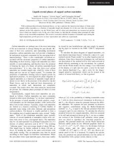
⬀Tr关 Im共 G o 兲兴 , which may then be integrated over the states in an energy window ⌬E, we are able to observe a relative increase in the electron density at the defect sites as compared to regions that are farther away. The increased electron density at the defects is also responsible for observed changes in the conductance during dc quantum transport. We first discuss the results for defects that form on pristine nanotubes. Figure 4 shows the simulated STM image of a 共10,10兲 tube under a 10% strain with a single 共5-7-7-5兲 defect. The images were simulated with two different tip biases of ⫹0.5 and -0.5 eV, respectively. Clearly, the most prominent features associated with this defect are the two rings located on the defect itself, which are in sharp contrast with the smoother, defect-free regions off to the side of the image. These rings correspond to the two pentagons of the 共5-7-7-5兲 geometry shown in Fig. 4共e兲. We have also plotted the plane-averaged electron density corresponding to states near the highest occupied molecular orbital 共HOMO兲 关panel 1共b兲兴 and the lowest unoccupied molecular orbital 共LUMO兲 关panel 1共d兲兴. Note that there is a strong peak in the electron
FIG. 4. Simulated STM image of a 共5-7-7-5兲 defect on a 共10,10兲 tube under 10% strain: 共a兲 Vti p ⫽⫺0.5 eV; 共b兲 planar average of the electron density for the HOMO states (Vti p ⫽⫺0.5 eV); 共c兲 Vti p ⫽⫹0.5 eV; 共d兲 planar average of the electron density from the LUMO states (Vti p ⫽⫹0.5 eV); 共e兲 atomic positions corresponding to the imaged tube.
density from the states close to the HOMO, reflecting the increase in electron density in the center of a 共5-7-7-5兲 defect. This change in the electronic density, and consequently in the electronic states close to the HOMO, is also reflected in the differential STM conductance spectra. In Fig. 5 we present dI/dV curves computed along a line parallel to the axis of the tube. Note the strong features that appear in the spectra close to the defect. These reflect the changes in the LDOS induced by the defect itself.
14 198
DANIEL ORLIKOWSKI et al.
FIG. 5. Differential STM conductance spectra computed along a line parallel to the axis of a 共10,10兲 tube with a 共5-7-7-5兲 defect. Upper panel: geometry of the tube and position of the tip in the simulated measurement 共a兲–共f兲. Lower panel: dI/dV curves corresponding to the marked locations.
If conditions for plastic behavior are fullfilled, then the two 共5-7兲 pairs that constitute the 共5-7-7-5兲 defect can separate and migrate as illustrated in Fig. 1共b兲. Figure 6 shows a sample STM image of such a case, probed at tip voltages of ⫾0.5 eV. Even in this case, the pentagons figure prominently, appearing as bright rings. Note also the clear asymmetry in the images under the two different bias voltages: the orientation in which the prominent rings stack changes with the sign of the bias voltage. For both biases, there is also an asymmetry between the regions to the left and right of the defects. We now turn to the STM images of defective nanotubes, which are formed via the addition of adatoms and addimers to the tubes. The STM images of tubes with single adatoms resemble those of the clean tubes, except for the presence of a broad, circular ‘‘white’’ patch marking the place where the adatom has been absorbed. More interesting are the images of a 共7-5-5-7兲 defect obtained via the adsorption of a C 2 dimer into a nanotube sidewall, shown in Fig. 7. Dimers can also form when two migrating adatoms attach themselves to the same hexagon, as was observed in molecular-dynamics simulations. In Fig. 7, panels 共a兲 and 共b兲 refer to such a defect on a 共10,10兲 armchair tube, while panels 共c兲 and 共d兲 show a similar case for the 共17,0兲 zigzag tube. Both tubes are under a 10% tensile strain. These STM images clearly do not display the same kind of features that are associated with the
PRB 61
FIG. 6. 共10,10兲 carbon nanotube under 10% strain after the separation of the 共5-7-7-5兲 defect into two distinct 共5-7兲 units. Here 共a兲 Vti p ⫽⫺0.5 eV; 共b兲 Vti p ⫽⫹0.5 eV; 共c兲 atomic positions corresponding to the image.
共5-7-7-5兲 defect, suggesting that the location of the two pentagons is crucial in the determination of the electronic response of the system. For both types of tubes, the 共7-5-5-7兲 defect appears brighter, since there is a slight outward relaxation of atoms due to the geometry of the defect. Moreover, the prominent rings observed in the case of the 共5-7-7-5兲 defect are absent. While an increase in the electronic density inside the defect region is detected, we also note that the region surrounding the defect appears somewhat depleted of electronic charge. Under strains of 5% or more, the 共7-5-5-7兲 defect undergoes a continuous evolution, ultimately leading to the formation of a short segment of a tube of altered helicity. STM images of a first set of these transformations are shown in Fig. 8. Now that the two back-to-back pentagons are separated, the familar ‘‘rings’’ associated with the pentagons emerge again. These defects induce local modulations along the direction of the zigzag bonds oriented 120° from the axis of the tube on the opposite side of the defect. The direction of these modulations changes sign upon changing the tip voltage bias. These features extend approximately 20 Å to either side of the defect. B. dc conductance of defective carbon nanotubes
Before discussing the conductance signatures of defective nanotubes, we briefly review quantum transport through
PRB 61
THEORETICAL STM SIGNATURES AND TRANSPORT . . .
FIG. 7. STM images and corresponding atomic positions for a C 2 dimer absorbed into different nanotubes: 共a兲 and 共b兲 show a 共10,10兲 tube; 共c兲 and 共d兲 a 共17,0兲 tube. All images are under a 10% strain and are taken with a tip bias of ⫹0.5 eV.
ideal nanotubes. At the Fermi level, metallic nanotubes are characterized by the crossing of two bands, so that the dc conductance in units of G ideal ⫽2e 2 /h⬇(12.9 k⍀) ⫺1 has a value of 2G ideal . For the 共10,10兲 armchair tube, there are no other bands available for the energy range 关⫺0.8,0.8兴 eV around the Fermi level, so that G is effectively a constant. At larger voltage biases, the electrons are able to probe different energy bands, giving rise to an increase in G that is proportional to the number of additional bands available for transport. The conductance therefore consists of a series of ‘‘down-and-up’’ steps, with the step positions correlating with the band edges which lead to peaks in the density of states 共DOS兲 plots. We now turn to the conductance signatures of the defective nanotubes and their correlations with the electronic properties of the tubes. Figure 9 shows the conductivity and DOS for a strained 共10,10兲 tube with either a 共5-7-7-5兲 or a 共7-5-5-7兲 defect. Note that in both cases there is a small
14 199
FIG. 8. STM images and corresponding atomic positions of defects that are formed when bonds emanating from the pentagons of a 共7-5-5-7兲 defect are rotated: 共a兲 and 共b兲 single bond rotation; 共c兲 and 共d兲 two bonds rotate to enclose two hexagons. The tubes are under a 10% strain and the images are for a tip with a ⫺0.5-eV bias voltage.
reduction in the conductivity plateau around the Fermi level. The 共5-7-7-5兲 defect also shows a marked decrease from its ideal, theoretical value near E⫽0.5 eV. This reduction in G is accompanied by an increase in the DOS and corresponds to the appearance of electronic states associated with the defect structure. The ring modulations observed in the STM images correlate also with the enhancement of the DOS and the decrease in the conductivity, while a smaller enhancement of the DOS results in a reduced prominence of the rings associated with the STM images. The 共7-5-5-7兲 defect shows a similar reduction in G, but the ‘‘dip’’ in this case is much closer to the band edges. The conductance and the DOS for the defects containing rotated hexagons are shown in Fig. 10. For the defect containing a single rotated hexagon, there is a pronounced decrease in the conductivity just below the Fermi level. The
DANIEL ORLIKOWSKI et al.
14 200
PRB 61
FIG. 9. 共a兲 Conductivity of 共10,10兲 defective nanotubes in units of 2e 2 /h: solid line, pristine nanotube; dotted line, 共5-7-7-5兲 defect; and long-dashed line, 共7-5-5-7兲 defect. 共b兲 The DOS for the case corresponding to 共a兲.
corresponding DOS shows a marked increase in the same region. Similar features are observed for other defects consisting of a larger number of rotated hexagons. However, the energy range over which the conductivity is decreased and the DOS is increased is much broader. To summarize, while each of the defects investigated has a definite effect on the conductance signature, there appears to be no overriding unique element that would allow for an unambiguous identification of any of the defects. C. Nanotube-based heterojunctions
As described previously, addimers on strained nanotubes lead to large-scale mechanical transformations of the tubes, ultimately resulting in extended defects that form different electronic heterojunctions.17 We have therefore investigated the STM images and G of such systems. In Fig. 11 we therefore show the simulated STM image of such a quenched heterojunction comprised of a metallic 共8,8兲 tube sandwiched between two insulating 共17,0兲 zigzag tubes. As before, the
FIG. 10. 共a兲 Conductivity 共units of 2e 2 /h) and DOS 共arbitrary units兲 for defective 共10,10兲 tubes with addimers: solid line, pristine tube; dotted line, one rotated hexagon; and long-dashed line, two rotated hexagons. Both defects show enhancemeents of the DOS below and above the Fermi level. The conductivity is diminished at the Fermi level to 1.15(2e 2 /h) for the case of a single, rotated hexagon as described in the text.
FIG. 11. STM images of 共17,0兲/共8,8兲/共17,0兲 heterojunctions: 共a兲 and 共b兲 show the STM image and the corresponding atomic geometry; 共c兲 and 共d兲 STM image and atomic configuration for the heterojunction for which the 共8,8兲 section has been artificially lengthened, as discussed in the text. Both STM images are for V ti p ⫽ ⫺0.5 eV.
high density of pentagons in the defect induces ring modulations in the image. The 共8,8兲 section of the tube at the center of the defect 共i.e., the quantum dot itself兲, is not readily discernable as a distinct entity. We attribute this to the strong influence of the 共5-7兲 pairs at the edge of the quantum dot, which overrides the influence of the relatively short segment of the 共8,8兲 tube. To better characterize a junction region, we have artificially extended the interior of the 共8,8兲 section, see Figs. 11共c兲 and 11共d兲. The 共8,8兲 segment is now much more visible, and the modulations reflect more of the underlying geometry of the armchair tube. We have also studied a prototypical metal/insulator/metal 共MIM兲 structure, which was constructed as follows: we cut the 共17,0兲/共8,8兲/共17,0兲 quantum dot, and then repositioned the atoms to form a 共8,8兲/共17,0兲/共8,8兲 MIM structure as shown in Fig. 12. Once again, the STM image is dominated by the ring modulations of the pentagons from the 共5-7兲 pairs that separate the defect from the rest of the tube. However, the main symmetry features of the zigzag tube are visible in the interior of the image.
PRB 61
THEORETICAL STM SIGNATURES AND TRANSPORT . . .
14 201
FIG. 14. Clean 共17,0兲 tube with bias voltage applied at the left end while the right end is fixed at zero voltage: 共a兲 V bias ⫽0 eV with V ti p ⫽⫺0.5 eV; 共b兲 V bias ⫽0 eV with V ti p ⫽⫹0.5 eV. For 共c兲 and 共d兲, V bias ⫽3.0 eV with V ti p ⫽⫿0.5 eV, respectively. Panels 共e兲 and 共f兲 correspond to V bias ⫽⫺3.0 eV with V ti p ⫽ ⫿0.5 eV, respectively.
FIG. 12. Images and atomic geometry of a 共8,8兲/共17,0兲/共8,8兲 MIM heterojunction: 共a兲 and 共b兲 show the STM image and corresponding atomic geometry; 共c兲 and 共d兲 show the STM image and geometry for which the 共17,0兲 tube in the MIM interior has been artificially enlarged. STM images in both cases are for V ti p ⫽ ⫺0.5 eV.
In general, neither the quantum dot nor the MIM show any conductivity within the range of the DOS gap of the ideal 共17,0兲 tube. However, in both cases, we observe DOS peaks within this energy gap, as shown in Fig. 13. These peaks are associated with localized states of discrete energies. As the inner section of the quantum dot is lengthened, there is a decrease in the height of these peaks, as well as an increase in their number. Similar features are observed in the case of the MIM structure. D. Effect of bias voltage across the nanotubes
As a final topic we present a brief discussion of simulated STM images of biased nanotubes. In principle, since an STM
tip accesses different local states, one can expect that a bias across a tube will significantly alter the STM images. While we have investigated several tubes of different helicity, the most pronounced effects were observed for the 共17,0兲 zigzag tube shown in Fig. 14. In the absence of a bias voltage, the asymmetries in the STM images depend solely on the probe tip voltage, as shown in Figs. 14共a兲 and 14共b兲, and these follow the trends previously discussed in the literature.30,31 For the images in Figs. 14共c兲 and 14共f兲, the voltage in the right-hand lead was fixed at zero, while the voltages in the left lead were shifted. In these images the bias voltage is reflected through the appearance of a small shift in the modulation along the length of the tube. This is most apparent for V tip ⫽⫹0.5 eV. Starting near the left lead, there is a ‘‘ramping down’’ effect over the length of the tube, which is related to the screening of the field. This effect is particularly noticeable when one compares Figs. 14共b兲 and 14共d兲. In the former, the image consists predominantly of ‘‘stripes’’ oriented in the vertical direction. In the latter case, the stripes are strongly modulated and appear as circles, particularly in regions that are close to the left lead. Only at the extreme right-hand side of the image are stripes similar to Fig. 14共b兲 recovered. Similar features are associated with Fig. 14共f兲, but in this case the effect is considerably less pronounced. Similar effects have also been noted for tubes with different helicities, both with and without defects. IV. SUMMARY
FIG. 13. 共a兲 DOS 共arb. units兲 for 共17,0兲 tubes and different quantum dot structures. In all cases 共a兲–共c兲, the solid line corresponds to the DOS of a pristine 共17,0兲 tube. Dotted lines correspond to the following defects: 共a兲 共17,0兲/共8,8兲/共17,0兲 quantum dot structure shown in Fig. 11共b兲; 共b兲 共17,0兲/共8,8兲/共17,0兲 structure for an elongated quantum dot structure shown in Fig. 11共d兲; and 共c兲 共8,8兲/ 共17,0兲/共8,8兲 MIM structure shown in Fig. 12共b兲.
In summary, we have investigated theoretically the STM and conductance signatures of two different types of defects that form in strained carbon nanotubes. The first set is based on the 共5-7-7-5兲 defect, which forms via a bond rotation and dominates the initial mechanical response of strained carbon nanotubes. The second set is associated with the presence of addimers on strained nanotubes. The addimers induce largescale transformations, ultimately forming extended defects that are in fact small segments of tubes of altered helicity, separated from the main tube via a sequence of 共5-7兲 pairs. Therefore, the combination of addimers and strain may well be useful in forming different electronic heterojunctions, including different quantum dots. The simulations show that these transformations are most promising for the (n,0) zigzag tubes. For these tubes, the addimers induce plastic behavior in a usable manner on what are otherwise brittle tubes. The simulated STM images of each of the defects are
14 202
DANIEL ORLIKOWSKI et al.
for the most part unique, and are dominated by ‘‘rings’’ that are associated with the pentagons belonging to the defect. These pentagons, in turn, correlate with the underlying geometry of the defect allowing for its identification. Unfortunately, the effect of the defects on the conductance is relatively modest, so that it is unlikely that one can associate a specific conductance signature with any given defect. As expected, defects usually decrease the conductance, which reflects an enhanced quantum scattering. Many of the defects also lead to significant ‘‘dips’’ in the conductance, either slightly above or below the Fermi level. These effects are due to defect-induced localized states, which show up as peaks in the local DOS and as rings associated with the STM images. We have also simulated STM images of different electronic heterojunctions, such as quantum dots and MIM’s of various sizes. These images are for the most part dominated by the 共5-7兲 pairs at the edges of these defects; the sandwiched tube only becomes apparent when the structure
1
For reviews, see for example, M.S. Dresselhaus, G. Dresselhaus, and P.C. Eklund, Science of Fullerenes and Carbon Nanotubes 共Academic Press, San Diego, 1996兲; Carbon Nanotubes: Preparation and Properties, edited by T. Ebbessen 共CRC Press, Boca Raton, FL, 1997兲; J. Bernholc, C. Roland, and B. Yakobson, Crit. Rev. Solid State Mater. Sci. 2, 706 共1997兲. 2 J.W. Mintmire, B.I. Dunlap, and C.T. White, Phys. Rev. Lett. 68, 631 共1992兲; N. Hamada, S.I. Sawada, and A. Oshiyama, ibid. 68, 1579 共1992兲; R. Saito, M. Fujita, G. Dresselhaus, and M.S. Dresselhaus, Appl. Phys. Lett. 60, 2204 共1992兲: Phys. Rev. B 46, 1804 共1992兲; 53, 2044 共1996兲. 3 X. Blase, L.X. Benedict, E.L. Shirleym, and S.G. Louie, Phys. Rev. Lett. 72, 1878 共1994兲; Y.A. Krotov, D.-H. Lee, and S.G. Louie, ibid. 78, 4245 共1996兲. 4 L. Chico, V.H. Crespi, L.X. Benedict, S.G. Louie, and M.L. Cohen, Phys. Rev. Lett. 76, 971 共1996兲; L. Chico, L.X. Benedict, S.G. Louie, and M.L. Cohen, Phys. Rev. B 54, 2600 共1996兲; V.H. Crespi, M.L. Cohen, and A. Rubio, Phys. Rev. Lett. 79, 2093 共1997兲. 5 ˜ oz, Phys. Rev. Lett. L. Chico, M.P. Lo´pez Sancho, and M.C. Mun 81, 1278 共1998兲. 6 W. Tian and S. Datta, Phys. Rev. B 49, 5097 共1994兲; R. Tamura and M. Tsukada, ibid. 55, 4991 共1997兲; 58, 8120 共1998兲; M.P. Anantran and T.R. Govindan, ibid. 58, 4882 共1998兲. 7 A.A. Farajian, K. Esfarjani, and Y. Kawazoe, Phys. Rev. Lett. 82, 5084 共1999兲. 8 M. Buongiorno Nardelli, Phys. Rev. B 60, 7828 共1999兲; M. Buongiorno Nardelli and J. Bernholc, ibid. 60, 16 338 共1999兲. 9 A. Rochefort, F. Lesage, D. Salahub, and Ph. Avouris, Phys. Rev. B 60, 13 824 共1999兲; A. Rochefort, D. Salahub, and Ph. Avouris, Chem. Phys. Lett. 297, 45 共1998兲. 10 C. Roland, M. Buongiorno Nardelli, J. Wang, and H. Guo, Phys. Rev. Lett. 84, 2921 共2000兲. 11 J.W.G. Wildoeer, L.C. Venema, A.G. Rinzler, R.E. Smalley, and C. Dekker, Nature 共London兲 391, 59 共1998兲; J.W. Odom, J.-L. Huang, P. Kim, and C.M. Lieber, ibid. 391, 62 共1998兲. 12 P.G. Collins, Z. Zettl, H. Bando, A. Thess, and R.S. Smalley, Science 278, 100 共1996兲; S.N. Song, X.K. Wang, R.P.H. Chang,
PRB 61
is sufficiently elongated. In the specific structures examined, there is no dc transport without shifting the Fermi level with a bias voltage, despite the significant number of states within the gap, which apparently are all localized. Finally, we note that it should be possible to investigate all of these effects experimentally. With the aid of nanomanipulators and other such devices, one can already study the mechanical/electrical properties of suspended and deposited nanotubes under a tensile load14共b兲,28,29 so that detailed information about the native defects of carbon nanotubes should become available in the near future. ACKNOWLEDGMENTS
This work was supported in part by Grant Nos. ONR N00014-98-1-0597 and NASA NAG8-1479. We also thank the North Carolina Supercomputing Center 共NCSC兲 for extensive computer support.
and J.B. Ketterson, Phys. Rev. Lett. 72, 697 共1994兲; L. Langer, L. Stockman, J.P. Heremans, V. Bayot, C.H. Olk, C. Van Haesendonck, Y. Bruynseraede, and J.-P. Issi, J. Mater. Res. 9, 927 共1994兲: L. Langer, V. Bayot, E. Grivei, J.-P. Issi, J.P. Heremans, C.H. Olk, L. Stockman, C. Van Haesendonck, and Y. Bruynseraede, Phys. Rev. Lett. 76, 479 共1996兲; S.J. Tas, M.H. Devoret, H. Dai, A. Thess, R.E. Smalley, L.J. Georliga, and C. Dekker, Nature 共London兲 386, 474 共1997兲; A. Bachtold, C. Strunk, J.-P. Salvetat, J.-M. Bonnard, L. Forro, T. Nussbaumer, and C. Schoenenberger, Nature 共London兲 397, 673 共1999兲. 13 A. Bezryadin, A.R.M. Verschueren, S.J. Tans, and C. Dekker, Phys. Rev. Lett. 80, 4036 共1998兲. 14 Z. Yao, H. Postma, L. Balents, and C. Dekker, Nature 共London兲 402, 273 共1999兲; S. Paulson, M.R. Falvo, N. Snyder, A. Helser, T. Hudson, A. Seeger, R.M. Talyor, II, R. Superfine, and S. Washburn, LANL e-print cond-mat/9905304. 15 A.J. Stone and D.J. Wales, Chem. Phys. Lett. 128, 501 共1986兲. 16 M. Buongiorno Nardelli, B.I. Yakobson, and J. Bernholc, Phys. Rev. B 57, R4277 共1998兲; M. Buongiorno Nardelli, B.I. Yakobson, and J. Bernholc, Phys. Rev. Lett. 81, 4656 共1998兲. 17 D. Orlikowski, M. Buongiorno Nardelli, J. Bernholc, and C. Roland, Phys. Rev. Lett. 83, 4132 共1999兲. 18 M. Ge and K. Sattler, Science 260, 515 共1993兲. 19 Z. Zhang and C.M. Lieber, Appl. Phys. Lett. 62, 2792 共1993兲. 20 C.H. Olk and J.P. Heremans, J. Mater. Res. 9, 259 共1994兲. 21 M. Bockrath, D.H. Cobden, P.L. McEuen, N.G. Chopra, A. Zettl, A. Thess, and R.E. Smalley, Science 275, 1922 共1997兲. 22 D.L. Carroll, Ph. Redlich, P.M. Ajayan, J.C. Charlier, X. Blase, A. De Vita, and R. Car, Phys. Rev. Lett. 78, 2811 共1997兲. 23 W. Clauss, D.J. Bergeron, and A.T. Johnson, Phys. Rev. B 58, R4266 共1998兲. 24 L.C. Venema, J.W.G. Wildo¨er, C. Dekker, G.A. Rinzler, and R.E. Smalley, Appl. Phys. A: Mater. Sci. Process. 66A, S153 共1998兲. 25 D.L. Carroll, Ph. Redlich, X. Blase, J.C. Charlier, S. Curran, P.M. Ajayan, S. Roth, and M. Ru¨hle, Phys. Rev. Lett. 81, 2332 共1998兲. 26 L.P. Biro´, P.A. Thiry, Ph. Lambin, C. Journet, P. Bernier, and A.A. Lucas, Appl. Phys. Lett. 73, 3680 共1998兲. 27 L.C. Venema, J.W.G. Wildo¨er, J.W. Janssen, S.J. Tans, H.L.J.T.
PRB 61
THEORETICAL STM SIGNATURES AND TRANSPORT . . .
Tuinstra, L.P. Kouwenhoven, and C. Dekker, Science 283, 52 共1999兲. 28 M.-F. Yu, O. Lourie, M.J. Dyer, K. Moloni, T.F. Kelly, and R.S. Ruoff, Science 287, 637 共2000兲. 29 D.A. Walters, L.M. Ericson, M.J. Casavant, J. Liu, D.T. Colbert, K.A. Smith, and R.E. Smalley, Appl. Phys. Lett. 74, 3803 共1999兲. 30 C.L. Kane and E.J. Mele, Phys. Rev. B 59, R12759 共1999兲. 31 V. Meunier and Ph. Lambin, Phys. Rev. Lett. 81, 5588 共1998兲; V. Meunier, P. Senet, and Ph. Lambin, Phys. Rev. B 60, 7792 共1999兲. 32 A. Rubio, D. Sanchez-Portal, E. Artacho, P. Ordejo´n, and J.M.
14 203
Soler, Phys. Rev. Lett. 82, 3520 共1999兲. A. Rubio, Appl. Phys. A: Mater. Sci. Process. 68A, 275-282 共1999兲. 34 J. Tersoff and D.R. Hamann, Phys. Rev. Lett. 50, 1998 共1983兲; Phys. Rev. B 31, 805 共1984兲. 35 J. Tersoff, Phys. Rev. Lett. 61, 2879 共1988兲; Phys. Rev. B 37, 6991 共1988兲; D. Brenner, ibid. 42, 9458 共1990兲. 36 S. Datta, Electronic Transport in Mesoscopic Systems 共Cambridge, University Press, Cambridge, 1995兲. 37 V.H. Crespi, L.X. Benedict, M.L. Cohen, and S.G. Louie, Phys. Rev. B 53, R13 303 共1996兲. 33