voltage controlled oscillator (VCO), voltage level converter and active pixel ...... circuits, like cross-coupled level converters (CCLC), single-supply diode voltage Limited buffer ... Several new level-converting flip-flop circuits are also proposed.
VARIABILITY-AWARE LOW-POWER TECHNIQUES FOR NANOSCALE MIXED-SIGNAL CIRCUITS Dhruva V. Ghai, B.E., M.Tech.
Dissertation Prepared for the Degree of DOCTOR OF PHILOSOPHY
UNIVERSITY OF NORTH TEXAS May 2009
APPROVED: Saraju P. Mohanty, Major Professor Elias Kougianos, Co-Major Professor Murali Varanasi, Committee Member Armin Mikler, Committee Member and Coordinator of Graduate Studies Krishna Kavi, Chair of the Department of Computer Science and Engineering Costas Tsatsoulis, Dean of College of Engineering Michael Monticino, Interim Dean of the Robert B. Toulouse School of Graduate Studies
Ghai, Dhruva V. Variability-aware low-power techniques for nanoscale mixed-signal circuits. Doctor of Philosophy (Computer Science and Engineering), May 2009, 131 pp., 27 tables, 63 illustrations, 130 references. New circuit design techniques that accommodate lower supply voltages necessary for portable systems need to be integrated into the semiconductor intellectual property (IP) core. Systems that once worked at 3.3 V or 2.5 V now need to work at 1.8 V or lower, without causing any performance degradation. Also, the fluctuation of device characteristics caused by process variation in nanometer technologies is seen as design yield loss. The numerous parasitic effects induced by layouts, especially for high-performance and high-speed circuits, pose a problem for IC design. Lack of exact layout information during circuit sizing leads to long design iterations involving time-consuming runs of complex tools. There is a strong need for low-power, highperformance, parasitic-aware and process-variation-tolerant circuit design. This dissertation proposes methodologies and techniques to achieve variability, power, performance, and parasitic-aware circuit designs. Three approaches are proposed: the single iteration automatic approach, the hybrid Monte Carlo and design of experiments (DOE) approach, and the cornerbased approach. Widely used mixed-signal circuits such as analog-to-digital converter (ADC), voltage controlled oscillator (VCO), voltage level converter and active pixel sensor (APS) have been designed at nanoscale complementary metal oxide semiconductor (CMOS) and subjected to the proposed methodologies. The effectiveness of the proposed methodologies has been demonstrated through exhaustive simulations. Apart from these methodologies, the application of dual-oxide and dual-threshold techniques at circuit level in order to minimize power and leakage is also explored.
Copyright 2009 by Dhruva V. Ghai
ii
ACKNOWLEDGMENTS The writing of a dissertation is not possible without the personal and practical support of numerous people. I would like to express my profound gratitude and deep appreciation to my major professor, Dr. Saraju P. Mohanty, and my co-major professor, Dr. Elias Kougianos, for supervising my overall research and guiding me throughout the course of my Ph.D. Without their help and guidance this research would not have been possible. The numerous brainstorming sessions with them helped me to not only embolden my knowledge but also to cultivate new ideas. I am grateful to my doctoral committee member, Dr. Armin Mikler, for offering his insight and spending his valuable time in reviewing my dissertation. I also thank Dr. Murali Varanasi for being on my doctoral committee and offering guidance. I would like to acknowledge the National Science Foundation for funding my research through NSF award number 0702361. Thanks to my colleagues at VDCL (VLSI Design and CAD Laboratory), Garima, Ruchi, Manish and Sahasan, for lively discussions, insightful comments, and honest opinions on my research. Finally, I would like to thank my family, who encouraged me to join the Ph.D. program at UNT and supported me throughout.
iii
TABLE OF CONTENTS Page ACKNOWLEDGMENTS……………………………………………………………….……. iii LIST OF TABLES …………………………………………………………………..………..viii LIST OF FIGURES…………………………………………………………………………….. x Chapter 1. INTRODUCTION AND MOTIVATION …………………………………………….….….1 1.1. Issues Faced by Digital, Analog, and Mixed-Signal Circuits ………………………...….3 1.1.1. Technology Scaling…………………………………………………………………. 3 1.1.2. Power Performance ………………………………………….………………….……5 1.1.3. Process Variation …………………………………………….………………………5 1.1.4. Parasitics…………………………………………………….………………………..6 1.1.5. Temperature Variation …………………………………….…………………………6 1.2. Organization of This Dissertation ………………………………………………………...7 2. THEORETICAL BACKGROUND..…………………………………………………..……...9 2.1. Emerging Technologies …………………………………………………………………...9 2.1.1. Nanoscale CMOS (Nano-CMOS)…………………………………………….……..11 2.1.2. High-κ/Metal Gate………………………………………………………………….. 15 2.1.3. Fin FET/Dual-Gate FET …………………………………………………………….16 2.1.4. Carbon Nanotube (CNT) ……………………………………………………………18 2.2. Power Leakage and Delay Models……………………………………………………… 20 2.2.1. Dynamic Power ……………………………………………………………………..21 2.2.4. Total Power Dissipation……………………………………………………………. 23 2.2.5. Delay Model ………………………………………………….……………………..23 iv
2.3. Low-Power Design Techniques…………………………………………………………. 24 2.3.1. Dual Threshold (Dual V T ) …….……………………………………………………..26 2.3.2. Dual Oxide (Dual T ox ) ……….………………………………………………………26 2.3.3. Dual Supply (Dual V dd )……….…………………………………………………….. 27 3. RELATED PRIOR RESEARCH …………………………………………………………….29 3.1. Dual Supply and Dual Threshold ….……………………………………………………..29 3.2. Dual Oxide………………………………………………………………………………. 30 3.3. Process Variation………………………………………………………………………... 31 3.4. Parasitics………………………………………………………………………………… 31 3.5. Literature Related to Mixed-Signal Circuits ……………………………………….…….32 3.5.1. Analog-to-digital Converters …………………………………………………….….32 3.5.2. Voltage-controlled Oscillators ………………………………………………………33 3.5.3. Level Converters……………………………………………………………………. 35 3.5.4. Active Pixel Sensors ………………………………………………………………...37 4. PROPOSED LOW-POWER DESIGN AND OPTIMIZATION METHODOLOGIES……. 39 4.1. Issue of Process Variation……………………………………………………………….. 39 4.2. Single-Iteration Automatic Approach…………………………………………………… 41 Algorithm Used for Optimization in the Single-iteration Automatic Approach…………….. 44 4.3. Hybrid Monte Carlo and Design of Experiments (DOE) Approach……………………. 46 Proposed Monte Carlo/DOE-based Algorithm for Variability-Aware Optimization ………...46
v
4.4. Corner-based Methodology ……………………………………………………………...49 5. CASE STUDIES USING SAMPLE DIGITAL, ANALOG AND MIXED-SIGNAL CIRCUITS ………………………………………………………………………………………51 5.1. Analog-to-digital Converter............................................................................................... 51 5.1.1. Comparator Design ………………………………………………………………….52 5.1.2. 1 of n Code Generator Design……………………………………………………… 54 5.1.3. NOR ROM Design…………………………………………………………….……. 55 5.1.4. Physical Design and Characterization of ADC……………………………..………. 56 5.1.5. Transistor-Level Design and Characterization of the ADC at 45 nm Technology ………………………………………………………….63 5.2. Voltage-controlled Oscillator (VCO) ……………………………………………………68 5.3. Universal Voltage Level Converter (ULC) ………………………………………………71 5.3.1. Design of ULC ………………………………………………………………………72 5.4. Active Pixel Sensor (APS) ……………………………………………………………….80 5.4.1. Models for the Figures of Merit of the APS array………………………………….. 84 6. PROCESS VARIATION ANALYSIS AND DESIGN OPTIMIZATION ………………….86 6.1. Analog-to-digital Converter (ADC) ……………………………………………………..86 6.1.1. Process and Supply Variation ……………………………………………………….86 6.1.2. Temperature Variation Characterization ……………………………………………88 6.2. Voltage-controlled Oscillator (VCO) ……………………………………………………89 6.2.1. Parasitic-aware Optimization ………………………………………………………..89 6.2.2. Process Variation Study …………………………………………………………….93 6.2.3. Parasitic- and Process-variation-aware Optimization ……………………………….97
vi
6.2.4. Physical Design of the Optimal VCO ……………………………………………...102 6.3. Universal Voltage Level Converter (ULC)…………………………………………….. 102 6.3.1. Dual T ox Technique ………………………………………………………………...102 6.3.2. Dual V T Technique …………………………………………………………………104 6.3.3. Characterization ……………………………………………………………………105 6.4. Active Pixel Sensor (APS) ……………………………………………………………...109 7. CONCLUSION AND FUTURE WORKS …………………………………………………119 7.1. Summary ………………………………………………………………………………..119 7.2. Conclusions ……………………………………………………………………………..119 7.3. Future Research ………………………………………………………………………...122 REFERENCES ………………………………………………………………………………..123
vii
LIST OF TABLES Page Table 3.1. Comparative Perspective of Existing 6-bit Flash ADCs …………………………….33 Table 3.2. VCO Performance Comparison ……………………………………………………...34 Table 3.3. Comparative Perspective of Level-converters ………………………………………37 Table 3.4. Comparative Perspective of Existing APS Designs …………………………………38 Table 5.1. Componentwise Power Consumption of ADC ……………………………………....61 Table 5.2 ADC Performance with Nominal Supply and Threshold Voltages …………………..62 Table 5.3. Comparator Transistor Sizes for Input Voltage Range at 45 nm Technology ……….64 Table 5.4. ADC Performance at 45 nm Technology ……………………………………………67 Table 5.5. Truth Table for Functionality of Baseline ULC Design ……………………………..72 Table 5.6. Transistor Sizes ………………………………………………………………………81 Table 5.7. Baseline Characterization of APS Array …………………………………………….85 Table 6.1 Process Variation Results …………………………………………………………….87 Table 6.2. Supply Voltage Variation Results ……………………………………………………88 Table 6.3. Effect of Temperature Variation ……………………………………………………..89 Table 6.4. Final Values of the Design Variables fro Parasitic-aware Design …………………..91 Table 6.5. Measured Performance of the Parasitic-aware VCO ………………………………..91 Table 6.6. Mean and Standard Deviation of Oscillation Frequency for 5 Cases ………………..96 Table 6.7. Frequency Discrepancy and Worst-case Process Values for a Target Frequency ≥ 2 GHz ……………………………………………………………………………………………...97 Table 6.8. Final Optimal Values for Design Variables ………………………………………….99 Table 6.9. Performance Summary of the Parasitic and Process-variation-aware VCO ………..101 viii
Table 6.10. Final Values of the Optimization Parameters Using the DOX-CMOS Technique .103 Table 6.11. Optimal Design Variable Values Using the DVTCMOS Technique ……………..104 Table 6.12. Power Consumption ……………………………………………………………….109 Table 6.13. Monte Carlo Simulation Results …………………………………………………..113 Table 6.14. Baseline and Optimal Values of the Figures of Merit …………………………….117 Table 7.1. Comparison of Results of Optimization Approaches ………………………………121
ix
LIST OF FIGURES Page Figure 2.1. Various leakage currents in a nanoscale CMOS transistor. ………………………...14 Figure 2.2. Structure of high-κ metal gate transistor. …………………………………………...16 Figure 2.3. Structure of the fin FET transistor. ………………………………………………….18 Figure 2.4. Structure of a CNT transistor. ………………………………………………………20 Figure 4.1. Standard IC design flow. ……………………………………………………………42 Figure 4.2. Proposed parasitic-aware IC design flow. …………………………………………..43 Figure 4.3 Parasitic- and process-variation-aware IC design flow ……………………………...45 Figure 4.4. Aim of the hybrid Monte Carlo and DOE-based optimization. …………………….49 Figure 4.5. The corner-based methodology used for process variation. ………………………...50 Figure 5.1. High-level representation of the ADC. ……………………………………………...52 Figure 5.2. Detailed block diagram of the flash ADC. ………………………………………….52 Figure 5.3. Threshold inverter (TI) comparator. ………………………………………………...54 Figure 5.4. Complete circuit diagram for a 3-bit flash ADC shown for brevity. ………………..55 Figure 5.5. Complete layout of the 90 nm ADC. ………………………………………………..56 Figure 5.6. Functional simulation of the 6-bit ADC operating at 1 GS/s. ………………………57 Figure 5.7. INL plot of the ADC. ………………………………………………………………..59 Figure 5.8. DNL plot of the ADC. ………………………………………………………………59 Figure 5.9. FFT plot of the ADC at a sinusoidal input frequency f in of 1 MHz for SNDR calculation. ………………………………………………………………………………………60 Figure 5.10. Instantaneous power plot of ADC with a load capacitance of 100 fF. …………….62 Figure 5.11. Functional simulation of the ADC at 45 nm mode. ………………………………..64 x
Figure 5.12. INL plot of the ADC at 45 nm node. ………………………………………………65 Figure 5.13. DNL plot of the ADC at 45 nm node. ……………………………………………..66 Figure 5.14. SNDR plot of ADC at 45 nm node. ……………………………………………….66 Figure 5.15. Instantaneous power plot of the ADC at 45 nm node. …………………………….67 Figure 5.16. Nominal-case logical design of the VCO. …………………………………………69 Figure 5.17. High level representation of the ULC. …………………………………………….71 Figure 5.18. Schematic logical block diagram of the baseline (unoptimized) ULC. ……………72 Figure 5.19. Circuit used for pass/block ………………………………………………………...73 Figure 5.20. Functional simulation result of up-converter circuit. ……………………………...74 Figure 5.21. Down-converter circuit. ……………………………………………………………75 Figure 5.22. Functional simulation of down-converter circuit. …………………………………75 Figure 5.23. Transistor-level realization of the baseline design of the ULC with 32 transistors. 76 Figure 5.24. Functional simulation for pass/block circuit at V ddl = 1.02 V, V ddh = 1.2 V and load = 45 fF. ……………………………………………………………………………………………77 Figure 5.25. Transistor-level realization of the baseline design of the ULC with 32 transistors. 78 Figure 5.26. Transistor-level circuit realization of the area optimal ULC. ……………………..79 Figure 5.27. Functional simulation of the area optimal ULC. …………………………………..79 Figure 5.28. Circuit diagram of an APS. ………………………………………………………..81 Figure 5.29. An 8 × 8 APS array constructed by using a collection of APS. …………………...82 Figure 5.30. Circuit diagram of an APS. ………………………………………………………..83 Figure 5.31. Circuit simulation of the 8 × 8 APS array. ………………………………………...83 Figure 6.1. Corner methodology used for the process variation study. …………………………87 xi
Figure 6.2. Comparison of frequency-voltage characteristics of the logical design and parasitic extracted physical design of the VCO. …………………………………………………………90 Figure 6.3. Final layout of the VCO optimized for parasitic-aware design flow. ………………92 Figure 6.4. Frequency-voltage transfer characteristics of the VCO optimized for design flow accounting for parasitics. …………………………………..……………………………………92 Figure 6.5. Statistical V dd variation. …………………………………………………………….94 Figure 6.6. Statistical V Tnmos variation. ………………………………………………………….94 Figure 6.7. Statistical V Tpmos variation. …………………………………………………………..95 Figure 6.8. Statistical simultaneous T oxnmos + T oxpmos variation. …………………………………95 Figure 6.9. V dd + V Tnmos + V Tpmos + T oxnmos + T oxpmos variation. …………………………………96 Figure 6.10. Comparison of frequency-voltage characteristics of the logical design, parasitic extracted physical design, and parasitic extracted physical design subjected to worst-case process variation. …………………………………………………………………………………...……98 Figure 6.11. Final VCO layout optimized for parasitic- and process-variation-aware design flow.…………………………………………………………………………………………….100 Figure 6.12. Frequency-voltage transfer characteristics of the VCO optimized for design flow accounting for parasitics and process variation. …………………………………………….…101 Figure 6.13. Parametric analysis with input voltage sweep. …………………………………...107 Figure 6.14. Performance of the ULC under varying output capacitive load. …………………108
xii
Figure 6.15. Instantaneous power plot of the ULC at a load capacitance of 45 fF. Average power consumed = 19.89µW..………………………………………………………………………....109 Figure 6.16. Proposed design flow for optimal design of nano-CMOS APS array. …………...110 Figure 6.17. Distribution of (a) average power P APS and (b) output voltage swing V swing for the case V dd = V dd-H and T xo = T ox-L . ……………………………………………………………….112 Figure 6.18. Distribution of (a) average power P APS and (b) output voltage swing V swing for the case V dd = V dd-L and T xo = T ox-L . ……………………………………………………………….114 Figure 6.19. Distribution of (a) average power P APS and (b) output voltage swing V swing for the case V dd = V dd-L and T xo = T ox-H . ……………………………………………………………....114 Figure 6.20. Distribution of (a) average power P APS and (b) output voltage swing V swing for the case V dd = V dd-H and T xo = T ox-H . ……………………………………………………………….115 Figure 6.21. Pareto plots for (a) fP APS and (b) fV swing . …………………………………………..117 Figure 6.22. Flowchart of the proposed algorithm. ……………………………………………118
xiii
CHAPTER 1 INTRODUCTION AND MOTIVATION The demand for low-power consuming circuits is increasing with the requirements for personal computing devices and wireless communications equipment. Several factors, such as battery life, heat dissipation, packaging costs, environmental concerns, and reliability issues are driving this demand [83]. Mechanisms such as voltage reduction, frequency scaling, and clock gating are helpful in reducing power consumption of the target systems for different applications [85]. Power management is fast becoming one of the most critical design constraints in the world of integrated circuit (IC) designers. New 90 nanometer (nm) processes deliver greater silicon (Si) performance and integration, but battery technology has not kept up. To compensate, new design techniques are being developed to address the need for low-power silicon. Dynamic power management techniques using variable supply voltage (variable V dd ) are popular for system-level power reduction, and multiple supply voltage (MSV) is a static solution for switching power reduction in application specific ICs (ASICs) [18]. The major components of total power dissipation in any circuit can be identified as P switching , the switching power dissipation; P short-circuit , the short-circuit power dissipation; and P leakage , the leakage power from various sources. Each one of these power dissipation sources is dependent on supply voltage, some linearly and some quadratically. For example, switching power has a quadratic relationship with the power supply voltage V dd . Hence, a significant amount of power can be saved by simply reducing the supply voltage V dd . However, the power reduction puts a strain on the performance targets. Since lowering the supply voltage slows down the speed at which transistors can switch, one must be selective in determining which parts of the design should have the voltage reduced (known as voltage scaling). Voltage scaling requires
1
partitioning of the design into voltage islands or voltage domains. Each domain operates at a different supply voltage depending on its timing characteristics [86]. The blocks that are timecritical in one domain operate at the standard supply voltage. The less time-critical blocks are aggregated into a second domain, with the voltage scaled down. A challenge with voltage scaling is the need to translate the voltages for the signals that interface between voltage domains. This translation is accomplished by inserting level shifters, which are special cells that perform voltage translation [57], and clamp cells to provide isolation. Basically, there are two types of voltage converters: level-up and level-down. A level-up converter is used as an interface in which low V dd cells (V ddl ) drive high V dd cells (V ddh ) in order to reduce the short-circuit power dissipation [129]. One application is the dual-V dd field programmable gate array (FPGA) fabric [78]. Level-down converter is required for switching power reduction, where the non-critical blocks of the circuit are made to operate at a lower-power supply voltage [57]. In the standby mode of a circuit, no active switching occurs, and all power dissipation is due to standby leakage. A simple power-saving scheme could be to shut off unused blocks in the standby mode. Portable electronic components such as cell phones, which are realized as systems on a chip (SoCs) and supplied with power from a single battery source require level converters. Such electronic devices often contain several sub-circuits, with each sub-circuit requiring a unique voltage level different from that supplied by the battery (sometimes higher or lower than the battery voltage). Level converters offer a method of generating multiple controlled voltages from a single, rather than multiple batteries, thereby saving space and cost to supply different parts of the device. They can also be effectively applicable for large-scale integration (LSI) high-speed input-output circuits, as an interface between internal and external buses as a server or
2
exchanger. They can also be used as an interface circuit between optical devices for optical communications [129] or as interfaces between different logic families. 1.1. Issues Faced by Digital, Analog, and Mixed-Signal Circuits The main issues faced by digital, analog, and mixed-signal circuits of today are as follows: 1.1.1. Technology Scaling A large number of SoCs are manufactured nowadays in the 90 nm process node, and the ramp up for 65 nm design has become more aggressive than expected. The 45 nm process design is following close behind, with early versions of design rules and process parameters already available [5, 4]. Intellectual property (IP) core providers are faced with the challenge of meeting analog performance in a technology that has been targeted for digital logic. New circuit design techniques that accommodate lower supply voltages necessary for portable systems also need to be integrated into the IP core. Systems that once worked at 3.3 volts (V) or 2.5 V now need to work at 1.8 V or lower without causing any performance degradation. The need for greater processing speed has designers craving smaller device geometries. Smaller devices provide higher packing density and lower overall power consumption, due to lower parasitics and lower supply voltages. This shortening of the minimum channel length has resulted in the reduction of power supply voltage to the 1 V - 0.7 V range. The SoC trend also forces analog circuits to be integrated with digital circuits. To keep up with the scaling of the minimum channel length and SoC trend, analog circuits need to be operated at low voltages, especially in portable devices. However, the minimum supply voltage for analog circuits predicted in the semiconductor road map [5] does not follow the reduction of digital supply voltage. Analog supply voltages between 1.8 V and 2.5 V are still being used with channel lengths of 0.18 micrometer (µm) and 0.13 µm
3
[30]. Hence, it is a great challenge to design low supply voltage operating analog/mixed-signal circuits while considering the relatively high threshold voltage of short channel length transistors. Another important consideration for an SoC is that the analog/mixed-signal circuits should be designed by using a standard complementary metal oxide semiconductor (CMOS) digital process without having process options such as deep n-well or on-chip inductors or varactors. Analog circuit designs often contain matched transistors [98]. The threshold voltage of a metal oxide semiconductor (MOS) transistor is defined as the gate voltage required to induce a channel for current flow through the transistor [99]. Matched CMOS transistors are designed to be necessarily identical. During fabrication, the threshold voltage of an MOS transistor is engineered to a desired voltage using processing. In a typical MOS field effect transistor (FET) process, ion-implanted charges are used to shift the threshold voltage. This processing step, called the threshold voltage adjustment implant, is random, consisting of varying energy levels of the implanted ions and subsequent temperature ramp step to diffuse the ions. The random nature of this process results in the random fluctuations in threshold voltage as a function of transistor area. Additionally, random variations in the lithography result in small geometric inaccuracies. The variation of the effective threshold voltage (V T ) increases as the transistor areas decrease. In CMOS analog circuits, it is the variation of the threshold voltages between two transistors rather than their absolute voltage values that is of interest for the majority of applications. Hence, it is essential to analyze the effect of threshold voltage mismatch on the analog circuit performance. Because the threshold voltage, mobility, and channel length of a device are sensitive to temperature variations [10], a temperature sensitivity analysis also needs
4
to be carried out. In addition, the power supply voltage variations in the analog design have been accounted for, to verify its system-on-chip capability. 1.1.2. Power Performance A dichotomy exists in the design of ICs: They must be simultaneously low power and high performance. Minimum power expenditure is joined at the hip to performance today. The goal of power-aware design is to minimize power consumption while meeting performance requirements. Therefore, as power dissipation increases, the cost of power delivery to the everincreasing number of transistors on a chip multiplies rapidly. Power conservation impacts every budget, whether technological or financial. Product acceptability, reliability, and profitability depend as much on power efficiency as they do on performance. There is a difference between low-power design and power-aware design [97]. Low-power design refers to minimizing power with or without a performance constraint. Power-aware design refers to maximizing some other performance metric, subject to a power budget. 1.1.3. Process Variation The fluctuation of device characteristics caused by process variation has considerably increased in nanometer technologies. Process variations can be classified into inter- and intra-die [92]. Inter-die variation, which comes from lot-to-lot, wafer-to-wafer, and within wafer, affects every device on a single chip equally. On the other hand, intra-die variation refers to device characteristics such as device geometry change, dopant density change, threshold voltage, gate oxide thickness, and circuit timing change, which vary from device to device within the same die. Some of the variations are random and some are systematic. Capturing and modeling the intra-die process variation becomes essential to device and interconnect extraction tools for accurate timing and power analysis. The standard design cycle
5
must include process variation in order to produce variation-tolerant physical designs. Just as in digital design where interconnect delays make or break a design, the move to 90 nm and lower process technologies means that the variations in process parameters have a resounding effect on the performance metrics of analog/mixed-signal, memory and radio-frequency (RF) circuits. Unlike a digital circuit, which is typically optimized only for speed and power, an analog circuit is designed to meet as many as 5 to 10 performance metrics. As a result, the impact of these process variations is seen as design yield loss, which in turn directly bites the bottom line of a company's profits. This loss calls for a proactive and a deterministic way to deal with performance and yield while in the design phase and not after the first silicon. 1.1.4. Parasitics Parasitic-aware optimization methodologies require that the parasitics be considered at the beginning of the design [96]. Where IC components are designed assuming ideal components, it is observed that parasitics have serious degrading effects at high frequencies. The only way to overcome these effects is to consider parasitics as an integral part of the circuit. Thus, parasitic-aware design and optimization are essential. If parasitics have an acute effect on the design, an early layout needs to be created so that the parasitics can be extracted and their effect estimated. Without that early layout-parasitic information, designers rely mostly on experience. If a design is understood well enough to know the sensitive nodes, dummy elements can be placed on those nodes to mimic the effect of real parasitics. This process is tedious and error-prone. Therefore, a methodology is required which can achieve the required performance while accounting for the parasitics. Hence, there is a need for a design methodology accounting for parasitics and process variation of general IC components. 1.1.5. Temperature Variation
6
Another emerging critical issue due to technology scaling is the effect of on-die temperature variation [21]. What was previously a second-order effect that could be adequately addressed with a few corner cases and guardbands has now become a first-order effect. Temperature interacts with a number of these other issues in ways that make analysis difficult. There's a need for new, temperature-aware design methodologies in order to produce properly functioning and reliable first silicon. Both power dissipation and operating frequency worsen at high temperatures because of the increase of leakage currents and the reduction of carrier mobility. The challenge for RF design is centering of a design including process, voltage and temperature (PVT) variations. By integrating temperature-aware capabilities into today's design flows, there is no need to rewrite the golden analysis standards that have been established for the past decade. Instead, through the use of tools that incrementally retrofit today's flows with temperature-aware data, the temperature effects can be fully accounted for. Applying thermal analysis reduces pessimism or risk associated with the assumption of a uniform on-chip temperature. A temperature-aware design flow is useful for existing technologies down to 90 nm, and is required for technologies below 90 nm. In summary, the demand for emerging application-specific, nanoscale mixed-signal SoCs which need process (threshold voltage mismatch) variation-tolerant low-power high-performance parasitic-aware mixed-signal circuitry and development of mature nano-CMOS processing technology has motivated this research. 1.2. Organization of This Dissertation This dissertation is organized as follows: Chapter 2 discusses the theory behind current state-of-art emerging technologies, the power leakage and delay models used in this dissertation, and the low-power design techniques implemented. Chapter 3 summarizes the various works
7
related to low-power design, parasitic-aware and process-variation characterization techniques, and mixed-signal circuits implemented in this dissertation. Chapter 4 discusses the issue of lowpower design in the presence of process variations and parasitics and presents the optimization methodologies used to achieve low-power, parasitic-aware and process-variation tolerant circuits. Chapter 5 presents the logical and physical design of mixed-signal circuits used as case studies in this dissertation, and their nominal characterization. Chapter 6 describes the application of the optimization methodologies discussed in chapter 4 to the circuits presented in chapter 5, thus demonstrating the effectiveness of these approaches. Finally, chapter 7 summarizes the results and concludes the dissertation with a mention of the future directions of research.
8
CHAPTER 2 THEORETICAL BACKGROUND This chapter presents the theoretical background related to the work presented in this dissertation. Section 2.1 discusses the current emerging technologies, considering the ongoing trends of the market. This discussion includes nanoscale complementary metal oxide semiconductor (nano-CMOS) transistors, high-κ metal gate transistors, fin field effect transistors (FET) (dual-gate FETs) and carbon nanotube transistors (CNT). Section 2.2 discusses the power leakage and delay models used for measurement. Finally, section 2.3 gives an overview of the existing low-power design techniques used in the market today and implemented in the work described in this dissertation. 2.1. Emerging Technologies Since their first demonstration in 1960 [5], planar silicon metal oxide semi-conductor field effect transistors (Si MOSFETs) have experienced a steady exponential downsizing of their critical dimensions. Over a period of 45 years, the printed gate lengths of the MOSFETs have been scaled down from 100 µm to 35 nm; the latter refers to the gate lengths for the 65 nm technology node devices in commercial microprocessors that are currently available. Because of a steady improvement of their performances through scaling, MOSFETs have become the leading integrated circuit (IC) technology for high-performance and low-power logic applications. Over this long period of development, the technology has faced numerous challenges, which were always solved by vigorous research, ingenious design, and brilliant engineering. The exponential scaling down of the feature sizes, and hence the exponential increase of the transistor count in an IC was first observed by Gordon Moore in 1965 [88]. His observation, which later became known as Moore's law, states that the number of transistors per 9
IC doubles every 24 months. Moore's law has been serving as the guiding principle for the semiconductor industry for over 30 years. According to projections by the International Technology Roadmap for Semiconductors (ITRS), by the middle of next decade, the printed gate length of the MOSFETs will be less than 10 nm [38]. Since no exponential can continue forever, sustaining Moore's law is becoming challenging for the planar bulk CMOS technology, for which the key technical issue for scaling devices below the 32 nm node is the high off-state leakage current [103]. The origin of this scaling limit for the single-gate, bulk CMOS technology can be traced back to the inherent poor electrostatic design of the planar device geometry and the poor transport properties of carriers in the Si channels. Consequently, an intense research effort, directed toward exploring new device designs and new channel materials for future logic technologies, has recently been undertaken. Dual-gate devices and carbon nanotube transistors [110] show promise for scaling beyond the planar bulk MOSFET limit. The electrostatic integrity of the nanoscale CMOS devices improves considerably when additional gates are included, such as for dual-gate or finFET devices. Because these non-planar devices are inherently resistant to short-channeleffects, it is widely believed that one of them will form the basic device architecture for future generations of CMOS devices. In order to sustain Moore's law for over four decades, nearly all materials and design aspects of the original MOSFET have been lost, except the use of Si-silicon dioxide (SiO 2 ) material system as channel material and gate insulator. Aggressive scaling of gate oxide has reduced its thickness to a present-day value of about 1 nm, and any further thinning is prohibitive because of oxide reliability issues and the exponential increase of leakage current from direct tunneling. Sustaining Moore's law, however, depends crucially on the gate insulator scaling; consequently, replacing SiO 2 with high-κ dielectric-metal gate stack is within sight [39].
10
Among all semiconductors, although Si has the poorest transport properties (mobilities and diffusion coefficients for electron and holes), its success as channel material is due to the excellent interface property of the Si-SiO 2 system. SiO 2 will almost certainly be replaced by high-κ gate dielectric in the near future. Research activity in this area has experienced a boom in recent years with many new devices and material systems now proposed. The following sections briefly describe the devices explored in this dissertation. 2.1.1. Nanoscale CMOS (Nano-CMOS) It has been overwhelmingly felt that mixed-signal electronics has been the driving force behind modern technological advances in the society. It has penetrated every walk of life and has been embedded into all our activities. Whether it is the built-in feature of an alarm clock in mobile phones that people wake up to in the morning or the sensor embedded into the microwave oven that heats a breakfast; the sleek, handheld personal digital assistant device or the laptop that keeps a busy executive on the move; or the latest MP3 player that accompany many joggers, everything has that “digital” tinge in it. In short, every accessory or gadget that used in daily life is becoming smaller, cheaper, more efficient, and more feature-packed; this is what “digital” equipment has come to mean to a general user. Demands for more and more features in every device have thus skyrocketed. Consequently, in recent years, there has been a phenomenal increase in the demand for low-power and high-performance digital devices. This market of digital electronics is driven by the prowess of an immensely versatile, efficient, and economical device called the CMOS. CMOS forms the backbone of today's circuits deploying very large scale integration (VLSI). The transistor-feature sizes have shrunk dramatically with the technology scaling. With the accompanying shrinking of feature size, a paradigm shift in the power profiles of the devices
11
has occurred. The leakage components of the fundamental CMOS device have changed exponentially, and each component of the total leakage has gained in relative importance. Thus, a drastic change has occurred in the leakage components of the device, both in the inactive as well as the active modes of operation. As the dimensions of the CMOS device reach nanometer ranges, dynamic power consumption remains almost unchanged; but leakage power dissipation increases significantly and becomes a large portion of the total power dissipation as the technology changes. This change has necessitated a critical analysis of the leakage components in the nanoscale CMOS VLSI devices and a concomitant need for the exploration of efficient reduction techniques of these leakage components, which continues to be dissipated even when a device is not doing any useful operation. Scaling of CMOS implies proportional reduction of the geometrical features as well as the parametric features (device characteristics) of the CMOS transistor. The idea of scaling began with the classical Moore's law, which had a phenomenal impact as a driving force for the entire semiconductor industry. CMOS scaling has become a very well-defined practice in the semiconductor industry. The design goals for scaling have been well defined for a long time. The main three typical goals of classical technology scaling are to • Reduce gate delay by about 30%, which results in an increase in an operating frequency of about 43% • Double the transistor density, which results in packing ever more components in the same chip (following Moore's law) • Reduce energy per transition by about 65% and thus save 50% of power (at a 43% increase in frequency)
12
Most of the goals have been maintained over all the years to a great benefit and have fueled market demand for portable devices. The scaling of CMOS has always beaten predictions and has advanced faster than predicted. The benefits of scaling have been manifold: • Decreasing device size • Increasing chip density and component density • Increasing performance and speed • Decreasing cost • Decreasing supply voltage • Decreasing power requirement However, there are some obvious roadblocks that can be credited to scaling: • Tremendous increase in power density in a chip • Issues in reliability and robustness • Ever-increasing mask costs and fabrication issues • Tremendous increase in complexity • Decreasing design flexibility • Random dopant fluctuations • Increasing process variations at nano levels • Increased likelihood of soft errors The channel length of a device represents the technology node that a particular process follows. The current industrial processes now are inching down to reach the nanometer level, where the channel length is of the order of a fraction of a micron. Industry has already put 45 nm node process into production. However, at these nanoscale levels, the channel is much shorter than the conventional channel length, and the device characteristics are very much affected by 13
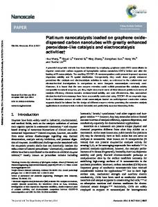
these shorter channel lengths. A number of adverse effects peculiar to scaling which result in a significantly reduced channel length are identified as short channel effects (SCEs). These SCEs mostly pertain to the power dissipation or leakage characteristics of the nanoscaled CMOS device. There are several forms of leakage currents (figure 2.1) in a short-channel nanometer transistor [103]: • I 1 : Drain to source active current (ON state) • I 2 : Drain to source short-circuit current (ON state) • I 3 : Subthreshold leakage (OFF state) • I 4 : Gate oxide tunneling leakage (ON and OFF states) • I 5 : Gate current due to hot carrier injection (ON and OFF states) • I 6 : Channel punch through current (OFF state) • I 7 : Gate-induced drain leakage (GIDL) (OFF state) • I 8 : Reverse biased p-n junction leakage (ON and OFF states)
Figure 2.1. Various leakage currents in a nanoscale CMOS transistor. Each power component has several forms and origins as they flow between different terminals and in different operating conditions of a transistor, as shown in figure 2.1. These 14
SCEs, among others, are gaining prominence with the phenomenon of scaling. To overcome these SCEs, the ITRS roadmap envisions that high-performance CMOS circuits will require ultra-low gate oxide thickness [5]. However, such devices will be susceptible to a more profound leakage mechanism because of tunneling through the gate oxide (I gate ) [29]. Thus, there is a critical need for analysis, explanation, and characterization of the various tunneling mechanisms, targeted toward design for manufacturing (DFM) and process variation modeling. 2.1.2. High-κ/Metal Gate Aggressive scaling of SiO 2 has been going on for the past 15 years for low-power, highperformance CMOS transistor applications [38]. Recently, SiO 2 with a physical thickness of 1.2 nm was implemented in the 90 nm logic technology node. In addition, research transistors with 0.8 nm (physical thickness) SiO 2 have been demonstrated in the laboratory. However, continual gate oxide scaling will require high-κ gate dielectric (κ being the dielectric constant) since the gate oxide leakage in SiO 2 is increasing with reducing physical thickness and SiO 2 will eventually run out of atoms for further scaling. The majority of the high-κ gate dielectrics investigated are based on hafniun oxide (HfO 2 ) and zirconium oxide (ZrO 2 ) [39]. Metals are being evaluated as the gate electrodes for the high-κ gate dielectrics. The use of high-κ serves the dual purpose of scaling the device as well as reducing gate leakage. Hence, high-κ metal gate transistors serve as a good alternative to classical CMOS transistors in nanoscale technologies. The structure of a high-κ metal gate transistor is shown in figure 2.2.
15
Figure 2.2. Structure of high-κ metal gate transistor. 2.1.3. Fin FET/Dual-Gate FET General MOSFET at a submicron level is suffering from several submicron issues like SCEs and threshold voltage variation. Fin FET is proposed to overcome the SCEs. The siliconon-insulator (SOI) process is used to fabricate fin FET. This process ensures the ultrathin specifications of the device regions. In fin FET, electrical potential throughout the channel is controlled by the gate voltage. This control is possible because of the proximity of the gate control electrode to the current conduction path between the source and the drain. These characteristics of the fin FET minimize the SCE [105]. Advantages of the fin FET over its bulkSi counterpart are as follows: • Conventional MOSET manufacturing processes can also be used to fabricate fin FET • Fin FET provides better area efficiency than MOSFET • Mobility of the carriers can be improved by using the fin FET process in conjunction with the strained Si process The silicon on insulator (SOI) process is used to manufacture fin FET. A single polysilicon layer is deposited over a fin. Thus polysilicon straddles the fin structure to form perfectly aligned gates. Here fin itself acts as a channel and it terminates on both sides of source and drain. In general MOSFET device, over the Si substrate poly-Si gate is formed. Poly-Si gate
16
controls the channel. Straddling of poly-Si gate over the Si fin gives efficient gate-controlled characteristics compared to MOSFET. Since gate straddles the fin the length of the channel is same as that of width of the fin. As there are two gates effectively around the fin, the width of the channel is equivalent to twice the height of the fin; i.e., W = 2 × h. A term called “fin pitch" is used to define the space between two fins. The height of the fin FET is equivalent to the width of the MOSFET. If W is the fin pitch, then to attain the same area efficiency required, fin height is W/2. But practical experiments have shown that fin height can be greater than W/2 for a fin pitch of W; thus, fin FET achieves more area efficiency than MOSFET. SOI technology is used for the fabrication of fin FET. In SOI technology, an insulator, SiO 2 , isolates the bulk from the substrate. An extremely shallow junction is formed because of the depth limitation put by the insulator. The dielectric isolation and elimination of the latch-up problem are the advantages of the SOI process. In the Fin FET fabrication process, silicon nitride (Si 3 N 4 ) and SiO 2 are deposited on a thin SOI layer. Electron beam lithography is used to form a Si fin. Channel length and channel width are determined by the accuracy of the fin. Poly-Si with pentavalent impurities and the oxide layer are deposited over the Si fin. The source and drain regions are separated and insulator spacers are formed. Then the etching process is carried out on a spacer until a Si fin is reached. Gate is formed by depositing the gate layer. Silicidation is performed to decrease the high-source drain resistance which is formed because of very thin layers of source and drain. The structure of fin FET is shown in figure 2.3.
17
Figure 2.3. Structure of the fin FET transistor. 2.1.4. Carbon Nanotube (CNT) Research within the computing industry continues to focus on downscaling the existing CMOS architectures. However, several problems arise when CMOS transistor feature sizes drop below 45 nm; these problems prevent manufacturers from fabricating improved VLSI designs using these nanoscale transistors. On the other hand, CNT devices show either only a fraction of these unwanted characteristics or exhibit no degree at all [11]. CNTs can be fabricated in either metallic or semiconducting configurations in which the current transport is ballistic, leading to carrier mobilities that are much higher than in Si. In addition, the absence of collision scattering in the one-dimensional crystalline structure of the CNTs results in current densities well in excess that of metals. Given their wire-like structure, CNTs can be used to fabricate transistors and interconnects, the two fundamental components of modern microelectronics technology. Among the preventative phenomena exhibited by nanoscale MOSFETs are the following: • High electric fields As feature sizes shrink to the nanometer level, MOSFETs require a nonlinear decrease in the power supply voltage as a function of channel length. The result is an increase in the magnitude of electric field across the gate oxide layer, which produces higher leakage
18
currents at the gate. This leakage current degrades performance and may drive the device into avalanche breakdown during which freely conducted electrons produce damaging current levels. The nanotube, however, acts as a quasi-one-dimensional path and possesses no called bulk. Therefore, power supply voltage can be reduced linearly as a function of channel (or tube) length. • Threshold voltage Although desirable, reduction of the threshold voltage proportional to the downscale of the MOSFET channel is not possible because it is necessary to control the quiescent state power consumption. This power consumption is due primarily to leakage current through the device, which is mitigated by maintaining a high threshold voltage. The large V T , however, reduces the margins between saturation and cutoff states, and therefore the probability the device may enter a linear mode of operation. • Interconnect delays Any decrease in wire width leads to an increase in interconnect resistance, thereby increasing propagation delay. It turns out that the increase in interconnect delays is large compared to the corresponding increase in gate delay. Thus, continued downscaling will yield diminishing returns in speed, which may eventually curtail altogether. • Gate-oxide layer shrinking At 0.1 µm, CMOS devices require an oxide thickness of at least 3 nm. Such a thin oxide layer allows quantum tunneling and hence leakage current through the gate. Decreases in the gate oxide layer exacerbate this leakage and render further downscaling impractical. Thus, inefficient doping and the onset of quantum mechanical effects hinder CMOS device operation when fabricated at nanometer scales. The hardware industry is attempting to work around these
19
obstacles by engineering devices that compensate for quantum effects. CNTs eliminate these concerns and provide a means of meeting future demands for smaller, faster microelectronic devices. What remains is to master the CNT FET fabrication techniques and the work required to bring these techniques to production level. Thus, we see that CNT is a potential successor for CMOS in nanoscale technologies. The research described in this dissertation aimed to explore the design scenario when future, CNT will be used to design the circuits at nanometer levels. Figure 2.4 shows the structure of a CNT transistor.
Figure 2.4. Structure of a CNT transistor. 2.2. Power Leakage and Delay Models While the aggressive scaling of CMOS technology to ever smaller dimensions has enabled higher performance and integration levels, it has given rise to a plethora of new problems in the design of ICs. The reason for this rise is that the supply voltage has continually scaled down to reduce the dynamic power consumption. As the supply voltage is scaled down, the threshold voltage has to be reduced in the same proportion to maintain performance. Reduced threshold voltages and gate oxide thicknesses have caused an alarming increase in subthreshold 20
source-drain leakage and gate leakage power dissipation in both active and standby modes of operation. As a result, leakage power has become an increasingly important fraction of the total chip power in the current technology generation. In the past, the subthreshold leakage of transistors has been very small; but as transistors have been scaled down below the 100 nm node, leakage composes nearly 50% of the total power consumption. As threshold voltages are reduced, subthreshold leakage rises exponentially. Also at nanoscale technologies, gate-oxide leakage is comparable to subthreshold leakage. The subthreshold leakage problem has been widely researched in recent years, and several promising circuit techniques have been proposed for addressing it [43]. However, in future technology generations, gate leakage is expected to grow faster than subthreshold leakage since gate oxide thicknesses are being scaled at a much faster rate than supply or threshold voltages [5]. Furthermore, gate leakage is a problem when the transistor is in both the on and the off states, whereas subthreshold leakage dissipates power only when the transistor is off. In general, the requirements for minimizing subthreshold leakage are contradictory to those for reducing gate leakage because of their inherently different mechanisms. This contradiction makes the problem of total leakage reduction challenging and intriguing as it is necessary to suitably mitigate both of these leakage components based on their relative contributions. In the future, it is certain that most of the burden of dealing with total leakage reduction will fall to circuit techniques. The following subsections explain the power models that are referred for the power-delay optimization of circuits used in this dissertation. Design techniques for the reduction of leakage power should not affect design performance. Hence, I also considered a delay model. 2.2.1. Dynamic Power
21
The dynamic power consumption of a circuit is given as [99]: (1)
2 × f Pdynamic = α × C L × Vdd
where the α term is an activity factor that captures how many devices are active on any particular clock cycle, C L is the total switched capacitive load, V dd is the supply voltage, and f is the frequency of the clock. P dynamic term is derived from the equations for energy consumed in charging and discharging a capacitor. This power dissipation depends on loading condition not the device features. 2.2.2. Subthreshold Leakage The subthreshold leakage current (I sub ) through a MOSFET can be modeled as follows [1, 72]: (2)
− V Vgs − VT − Voff I sub = I 0 × 1 − exp ds × exp vtherm S × vtherm
where I 0 is a constant dependent upon device parameters for a given technology, v therm is the thermal voltage, V T is the threshold voltage, V off is the offset voltage which determines the channel current at V gs = 0, S is the subthreshold swing factor, V gs is gate-to-source voltage, and V ds is the drain-to-source voltage. Hence, if T ox is increased, the length (L eff ) is increased and/or the width (Weff ) of the transistors is reduced, there will be a reduction in the subthreshold current. 2.2.3. Gate-Oxide Leakage Gate-oxide leakage in a MOSFET due to direct tunneling can be modeled as follows [42, 109]:
22
(3)
J DT
3 V − B 1 − 1 − ox 2 φ ox 2 Vox × exp = A × Vox Tox Tox
where J DT is the direct tunneling current density, V ox is the potential drop across the thin oxide, and φox is the barrier height for the tunneling particle (hole or electron). A and B are physical parameters. From this expression, one can see that gate leakage is exponentially dependent on variations in T ox . Hence, if T ox is increased, there will be a reduction in the gate oxide leakage current. 2.2.4. Total Power Dissipation The total power of a circuit (P circuit ) can then be calculated as (4)
P circuit = P dynamic + P subthreshold + P gate-oxide
where P dynamic , P subthreshold and P gate-oxide can be calculated from equations 1, 2 and 3, respectively. Thus, we conclude that T ox , V T , and the geometry of a transistor play a crucial role in determining the power dissipation of a circuit. 2.2.5. Delay Model The delay of a device is approximately given as [109]:
(5)
C L × Vdd Delay = k × μ × ∈ox × Weff × (V − V )α dd T Tox Leff
where k = technology constant, µ is the electron surface mobility and α is the velocity saturation index, which varies from 1.4 to 2 for nanometer CMOS. The delay of circuits is generally calculated from the 50% level of the input swing to 50% level of the output swing. 23
2.3. Low-Power Design Techniques As seen in the section 2.1, power dissipation has become the most significant issue for consumers as well as designers for the nanoscale CMOS regime. As the demand for more and more portable battery-operated devices increases, the issue of low-power VLSI design becomes more critical. The reasons that why power becomes an issue can be summarized as follows: • With scaling, new and ever-more obtrusive forms of power leakage become prevalent • Static power consumption becomes as significant as dynamic power, implying that the device is dissipating half the power without doing any useful work • High-power dissipation increases the packaging and cooling costs, which are not economical even at higher technology nodes • Battery technology, like many other technologies, is not expected to keep pace with the scaling • Wasting precious power resources affects the environment • Scaling has resulted in manifold complexity in today's CMOS circuits; this issue, along with diverse and profound power leakage makes reliability and robustness of the device a prime concern. The various low-power techniques can be classified into two categories: (1) Structural Techniques • Voltage islands • Multi-threshold (V T ) devices • Minimized capacitance by custom design • Power-efficient circuits • Parallelism in micro-architecture 24
(2) Traditional Techniques • Clock gating • Power gating • Variable frequency • Variable voltage supply • Variable device threshold (V T ) The above techniques are also aimed at reducing dynamic power and leakage power: (1) Dynamic Power Reduction • Clock gating • Power-efficient circuits • Variable frequency • Variable voltage supply (2) Leakage Power Reduction • Minimized usage of low V T cells • Power gating • Back-biasing • Reduced dynamic power • Reduced oxide thickness (T ox ) • Use of fin FETs In this dissertation, I have used the dual-threshold, dual-oxide, and dual-supply techniques for power reduction. These techniques are described in detail in the following paragraphs.
25
2.3.1. Dual Threshold (Dual V T ) Foundries typically provide two V T process options: high and low V T . Having only two options forces the designer to optimize either for performance or power. Designers often use different V T transistors for different logic blocks and logic gates within a device. That is, designers can use a low V T , high-leakage transistors for the critical path where performance is a requirement, and high V T transistors in parts of the chip where performance is not critical. Since the leakage current is exponentially dependent on the threshold voltage, increasing the threshold voltage would decrease the leakage current substantially. However, the high-threshold-voltage devices have larger switching delays. The various leakage-current mechanisms and some leakage reduction techniques for CMOS circuits have been discussed in [63] and [103]. The techniques for reducing leakage power involve static and dynamic approaches. The dynamic approach, The dual V T (DVTCMOS) design technique, which is a static approach, has been widely used in the custom VLSI designs for reducing leakage power. The DVTCMOS implementation reduces both the active and the standby leakages. Further, there is no performance degradation in a DVTCMOS implementation for custom VLSI designs. This technique uses two kinds of transistors in the same circuit. Some transistors have a high threshold voltage, and other transistors have a low threshold voltage. The high-threshold-voltage transistors have less subthreshold leakage-power dissipation but also have a larger delay as compared to the lowthreshold-voltage transistors. 2.3.2. Dual Oxide (Dual T ox ) Leakage current is a primary concern for low-power, high-performance digital CMOS circuits for portable applications, and industry trends show that leakage will be the dominant component of power in future technologies. New leakage mechanisms, such as tunneling across
26
thin gate oxides, which lead to gate oxide leakage current (I gate ), are coming into play from the 90 nm node onwards. According to the ITRS, a high-performance CMOS device will require gate oxide thicknesses of 0.7 to 1.2 nm, thus leading to gate leakage due to carrier tunneling through the ultra thin layer of gate oxide [5]. The probability of electron tunneling is a strong function of the barrier height (i.e., the voltage drop across gate oxide) and the barrier thickness, which is simply T ox . A small change in T ox can have a tremendous impact on I gate . The other component of leakage, subthreshold leakage (I sub ), forms a reducing fraction of the total leakage as T ox is reduced, so that I gate becomes the dominant leakage mechanism at nanoscale. The dual oxide technique explores the use of dual T ox values for minimizing leakage minimization and maintaining performance at the same time. A higher oxide thickness (T ox-H ) leads to increased delay. The dual T ox technique involves higher oxide thickness (T ox-H ) assignment to transistors in the non-critical path and lower oxide thickness (T ox-L ) assignment to transistors in the critical path. Thus, by using this technique, one can suppress gate oxide leakage while maintaining the speed of the circuit. 2.3.3. Dual Supply (Dual V dd ) Although a dual V T design helps engineers minimize leakage of their designs, another technique, dual supply design, helps designers control dynamic power. Similar to dual threshold design, dual supply design enables designers to give the critical paths and blocks in their designs access to maximum voltage for the process and specification, but the designers then reduce the voltage for less power-hungry blocks. For example, a processor block may require a clock speed of 500 MHz, but a universal serial bus (USB) core may require only 30 MHz to comply with the USB protocol and thus require less voltage to run. So, if designers give the USB core only the power it needs, they can drastically reduce the overall power that the design consumes. To
27
implement the method, designers traditionally put level shifters between blocks that are running at different voltages. If there is a 0.9 V region on an IC design that is sending a signal to a 1.2 V region, it is necessary to put a level shifter between the two regions so that it is possible to boost it to the swing in voltage and control timing. Although a fairly simple concept, its implementation is more complex. First, designers must get used to dealing with multiple voltages on a die. There are also some fairly significant challenges on the tools front. Most commercial synthesis and physical-design tools can insert level shifters and can perform multivoltage, but creating a register transfer level (RTL) is a problem. Hardware description languages (HDLs) do not yet have a mechanism for describing power connectivity. This lack is one area that electronic design automation (EDA) vendors are addressing by trying to implement a low-power standard. Another emerging method that started in custom design but is making its way into application specific integrated circuit (ASIC) design is the use of parallelism with voltage scaling. Parallelism is done to get the performance up, and then voltage is scaled down to reduce the power and energy. If one looks at dynamic power, voltage is clearly where the biggest gains will be. Given a timing constraint of 2 ns, for example, one first overachieves the timing objective. In particular, parallelism is added to get the critical path down to 1.2 ns. Then, the voltage is scaled down to relax back to the 2 ns cycle time achievement is needed. The decrease in voltage more than compensates for the increase in area.
28
CHAPTER 3 RELATED PRIOR RESEARCH In this chapter, I present a survey of the current literature related to the research presented in this dissertation. Section 3.1 and section 3.2 deal with literature on low-power design techniques such as dual supply voltage (V dd ), dual threshold voltage (V T ), and dual oxide thickness (T ox ). Section 3.3 and section 3.4 discuss the current research on process variation and parasitic-aware research. This discussion is followed by current literature related to the mixedsignal circuits discussed in section 3.5. 3.1. Dual Supply and Dual Threshold The research using the dual V dd technique is quite mature, and several approaches have been proposed in the literature over the past several years [18, 86, 59]. Certain types of circuitry called level converters are used for this purpose. The transistors on critical paths are operated on a higher supply voltage (V ddh ), whereas transistors on the non-critical paths are operated on a lower supply voltage (V ddl ) [70, 57]. Dual V dd and dual V T designs are becoming increasingly popular because of the rising leakage current levels of ultra-small metal oxide semiconductor field effect transistor (MOSFETs) [34, 115]. Decreasing the supply voltage is an effective way of reducing power. However, the delay increase that is due to the reduction in supply voltage causes reduction in the throughput of the circuit. In order to maintain circuit speed, it is necessary to reduce V T . This reduction, however, leads to an exponential increase in leakage current. Setting some of the transistors to high V T and low V dd allows maintaining overall performance while reducing leakage current [113, 69, 114]. Multiple threshold CMOS has been used by Pant et al. [95] for subthreshold current reduction. Khouri and Jha [64] proposed a dual V T technique for subthreshold leakage analysis and reduction during behavioral synthesis, targeting the least used
29
modules as the candidates for leakage optimization. Gopalakrishnan and Katkoori in [51, 52] also use the multi-threshold CMOS approach for reduction of subthreshold current during highlevel synthesis and propose binding algorithms for power, delay, and area trade-off. They used a clique partitioning approach in [52] and a knapsack-based binding algorithm in [51]. In [35], Liu et al. applied probabilistic analysis to V T variation. Dual V T design methodology was analyzed in the presence of large variations in threshold voltage. In [7], a dual V T and dual T ox technique was applied to static random access memory (SRAM) in order to reduce leakage. In [71], a dual V T field program gate array (FPGA) architecture has been proposed in which the logic elements are used for dual V T assignment. In [33], Wei et al. tried to reduce the leakage power by using high V T transistors in the non-critical paths and low V T transistors in the critical paths. 3.2. Dual Oxide In [90], Mukherjee et al. have proposed a gate oxide leakage minimization approach using dual T ox and dual K. In [84], Mohanty et al. presented analytical models and a data-path scheduling algorithm for reduction of tunneling current. The heuristic assigns higher thickness resources to more leaky nodes (multipliers) but does not address the area overhead. In [75], Lee et al. developed a method for analyzing gate oxide leakage current in logic gates and suggested utilizing pin reordering to reduce gate leakage. In [29], Sultania et al. developed an algorithm to optimize the total leakage power by assigning dual T ox values to transistors in a given circuit. In [112], Sirisantana and Roy used multiple channel lengths and multiple gate oxide thickness for reduction of leakage. In [91], Mukhopadhyay et al. have carried out extensive modeling and estimation of total leakage current of complementary metal oxide semiconductor (CMOS) devices considering the effect of parameter variation. In [46], the authors proposed application of dual T ox technique at circuit level to power-hungry transistors of a given circuit.
30
3.3. Process Variation As the device technology scales down to nanometer region, intra-die variations such as gate oxide thickness (T ox ) and threshold voltage (V T ) variations have become as important as inter-die variation when analyzing circuit performance and predicting the yield of a chip [17, 13, 14, 117]. With rising concerns of intra-die variation, some of these investigations which modeled process variations and performed timing analysis have been proposed [28, 94, 36]. Supply voltage (V dd ) variations also need to be considered during performance estimation. Several research works address process variation in nano-CMOS circuits. In [66], a current-controlled oscillator was subjected to process variations. In [83], the authors showed the effect of simultaneous variation of supply and process parameters on power consumption of data-path components. In [82], the authors developed process variation aware component libraries. This work focused on behavioral (high-level) synthesis. An increase in the number of variation sources has led to even more corner cases that need to be simulated for each design. In [93], the authors have estimated that the 3-σ/µ variation for 65 nm process technology is as high as 30% for transistor channel length and transistor threshold voltage. Future processes could have even larger amounts of variation. 3.4. Parasitics Because of the high sensitivity of radiofrequency (RF) integrated circuit (IC) design to layout parasitics, a lot of research has been done in the parasitic-aware synthesis area to overcome degradations that prevent optimal performance [96, 12] because of device and package parasitics. Simulated annealing is proposed for synthesizing RF CMOS circuits in [22, 53, 68, 77, 20]. Optimization techniques such as particle swarm optimization are proposed for parasiticaware design in [23]. In [25], an inductor-capacitor (LC)-based, voltage-controlled oscillator
31
(VCO) has been subjected to a parasitic-aware synthesis. A parasitic- and process-aware design flow has been proposed in [48]. In [67], the center frequency has been optimized using a design of experiments approach. A simulation-based circuit synthesis example is presented in [130]. 3.5. Literature Related to Mixed-Signal Circuits The current literature on mixed-signal circuits is discussed in this section. Four mixedsignal circuits widely used for various applications in the electronics industry today are discussed: • Analog-to-digital converters • Voltage-controlled oscillators • Level converters • Active pixel sensors 3.5.1. Analog-to-digital Converters Analog-to-digital converter (ADC) design is a bottleneck in system-on-a-chip (SoC) design. There is a need for more sophisticated circuitry in terms of speed, area, noise immunity and adaptability to the digital process. Recent ADC literature deals with issues of comparator offset cancellation [26], using capacitive interpolation to eliminate power-hungry resistive ladders [30] or simplifying the comparator design [32]. In [108], an average termination circuit was proposed to reduce power consumption. The problem of metastability at high sampling speeds was addressed in [119]. The SoC integration problem faced by ADCs has not been given sufficient attention. In [127], the authors proposed a solution using the threshold inverting technique. In [111], Song et al. proposed an ADC operating at 1 V but the technology is not nano-CMOS. Low-voltage ADC designs generally need to use voltage-boosting techniques [6]
32
or low-threshold processes [41]. The authors in [45] proposed an ADC design at 45 nm, but it is not supported with the physical design. Table 3.1 compares the proposed ADC of this dissertation with other ADCs described in the current literature. For fair comparison, only 6-bit, flash-type architecture ADCs have been chosen. The table shows that the proposed ADC is suitable for nanoscale SoCs; has superior integral nonlinearity (INL) and differential nonlinearity (DNL) (expressed in least significant bit [LSB]) performance; and is a low-voltage, low-power, high-speed design. Table 3.1. Comparative Perspective of Existing 6-bit Flash ADCs Works
Technology(nm) DNL(LSB) INL(LSB) V dd (V) Power(mW) Rate(GS/s)
Geelen [44]
350
< 0.7
< 0.7
3.3
300
1.1
Uyttenhove[119]
350
--
--
3.3
--
1
Donovan [26]
250
--
--
2.2
150
0.4
Tseng [32]
250
< 0.1
< 0.4
2.5
35
0.3
Yoo [60]
250
--
--
2.5
66.87
1
Scholtens [108]
180
--
0.42
1.95
328
1.6
Sandner [30]
130
< 0.4