VariPipe: Low-overhead Variable-clock Synchronous Pipelines Navid Toosizadeh, Safwat G. Zaky and Jianwen Zhu Department of Electrical and Computer Engineering, University of Toronto, Toronto, Canada
[email protected],
[email protected],
[email protected] VariPipe over previous work is its lower clock generation overhead. In the case study presented in this paper, the overhead of the added clock generation circuit is only 2.6% in area and 3% in energy consumption for a VariPipe DLX processor. By comparison, Dean’s variable clocking approach uses duplicates of functional units, which double the area and energy consumption of the functional units. Both the VariPipe processor and Dean’s achieve the same performance improvement of 2X over conventional isochronous design. The desynchronization method introduces a 13.5% area overhead in a DLX processor [3]; the processor does not adjust its speed based on the operations in the pipeline and therefore its performance gain is limited. The VariPipe approach is based on a synchronous circuit implementation, and thus, many challenges in the design of asynchronous circuits are avoided. Also, it employs a simple design methodology using standard cells and conventional synchronous design tools, which allows designers to use the proposed approach in many applications. A comprehensive comparison to related work is presented in Section VIII. Section II describes the basic idea of the VariPipe approach and Section III explains the methodology in more detail. Timing constraints are given in Section IV. A design flow to implement VariPipe application specific integrated circuits (ASICs) is presented in Section V, which is demonstrated and evaluated through a microprocessor case study in Sections VI and VII.
Abstract— Synchronous pipelines usually have a fixed clock frequency determined by the worst-case process-voltagetemperature (PVT) analysis of the most critical path. Higher operating frequencies are possible under typical PVT conditions, especially when the most critical path is not triggered. This paper introduces a design methodology that uses asynchronous design to generate the clock of a synchronous pipeline. The result is a variable clock period that changes cycle-by-cycle according to the current operations in the pipeline and the current PVT conditions. The paper also presents a simple design flow to implement variable-clock systems with standard cells using conventional synchronous design tools. The variable-clock pipeline technique has been tested on a 32-bit microprocessor in 90nm technology. Post-layout simulations with three sets of benchmarks demonstrate that the variable-clock processor has a two-fold performance advantage over its fixed-clock counterpart. The overhead of the added clock generation circuit is merely 2.6% in area and 3% in energy consumption, compared to an earlier proposal that costs 100% overhead.
I. I NTRODUCTION The time required to complete an operation in any given stage of a pipelined system depends on the operation being performed. In a conventional synchronous system, the delay of the longest path of the pipeline under the worst processvoltage-temperature (PVT) corner is used to determine the clock frequency. However, the longest path of the system is not necessarily triggered in every cycle. Also, the system is normally operating under typical PVT conditions. Hence, there are many times when a frequency much higher than that derived under worst conditions is possible. This paper introduces a variable-clock synchronous pipeline design (VariPipe), in which the clock period is adjusted in each clock cycle based on the operations taking place in the pipeline stages. An on-chip clock generation circuit dynamically matches the delay of the current operations of the pipeline in every cycle. At the same time, the clock period automatically adjusts to the current PVT conditions. The proposed approach achieves better performance than isochronous clocking, while retaining the simplicity of synchronous system design. Other advantages of variable-clock synchronous pipelines include a reduction in electromagnetic noise and suitability for voltage scaling techniques. These features make variable clocking appealing for many applications including embedded systems and portable devices. Several studies have been published that address variablespeed pipelines, including Telescopic units [1] and a variableclock pipeline processor introduced by Dean [2]. Asynchronous design methodologies such as desynchronization [3] and Mousetrap [4] have also been proposed to achieve average-case performance. The main advantage of 978-1-4244-5028-2/09/$25.00 ©2009 IEEE
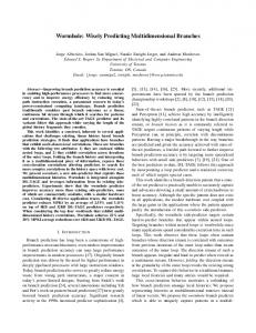
II. VARI P IPE : T HE IDEA Consider a pipelined system consisting of several pipeline stages of combinational logic, separated by pipeline registers. Each pipeline stage may have different modes of operation that are exercised by different instructions as they flow through the pipeline stage. For example, the execution stage of a RISC processor may execute different operations such as addition, bitwise logical operations, etc. The key observation is that these operations activate different paths and thus, they have different delays. In the isochronous clocking scheme, employed in today’s dominant EDA methodology, the clock period is constant, which means it must be longer than the delay of all possible operations in the pipeline at all times. VariPipe employs a clocking scheme in which the clock period continuously tracks the maximum delay under current PVT conditions for all operations currently being performed. As Fig. 1 shows, a variable delay is associated with each pipeline stage, and its delay is adjusted to match the delay of the current operation in the stage, as determined by the data in that stage’s input registers. When the delays of all pipeline 117
Critical path
Stage 1
Completion Detection Circuit for Stage 1 Stage 3
Shorter path
Variable Delay 1
Variable Delay 2
Input to the stage 1
Delay Selector
Operation Selection Table
S
Variable Delay 3
Toggle
Variable Delay
Clock Pulse Generator
C
Fig. 1.
CPW
VariPipe technique
Completion signal from Stage 1 Completion signal from Stage 2 Completion signal from Stage 3
Clock Pulse Generator
Fig. 2.
stages have elapsed, the clock pulse generator creates a new clock pulse. As a result, some clock cycles are shortened and the overall speed is increased. The variable delay unit is placed close to the corresponding datapath to be subject to the same PVT conditions. Note that although the proposed architecture benefits from its asynchronous nature, the use of asynchronous design is limited to the clock generation circuit, leaving the rest of the system still a synchronous circuit that can be designed, synthesized, and laid out using a traditional design flow.
Clock generation circuit
of delay values needed, delay values less than the delay of the shortest inevitable path in each profile are grouped and rounded up to the maximum value of the group. This simplifies the delay profile and the implementation of the clock generation circuit. C. Implementing the Clock Generation Circuit Fig. 2 shows the clock generation circuit, which is composed of two parts: the completion detection circuits and the clock pulse generator. The design of the clock generation circuit is based on the two-phase asynchronous design style [5] and thus inherits many properties from asynchronous systems. The completion detection circuit for each stage is composed of a variable delay, a toggle, an operation selection table and a delay selector. The delay selector reads appropriate signals from the inputs to the pipeline stage. It uses the operation selection table, which is ordered according to the delay values, to generate a onehot delay selection signal (S) to select the appropriate delay value. If the inputs to the pipeline stage activate more than one operation (e.g., in a complex multi-task stage), the delay corresponding to the operation with the longest delay is selected. When the clock pulse emerges from the variable delay element, it is converted to a level by the toggle before being sent to the C-element. Initially, all toggle elements are reset and so is the output of the C-element. After the reset is removed, all toggle elements change state causing the Celement to toggle its output, thus creating a clock pulse of width CPW at the output of the XOR. The clock pulse loads new values into the input registers of each pipeline stage. Note that the delay through the delay elements must be at least long enough for the corresponding delay-selection signals to become valid. After a delay matching the operation with the longest delay currently in the stage, the toggle changes state. When all stages have switched to the new state, the C-element toggles creating a new clock pulse.
III. D ESIGN M ETHODOLOGY In this section, the methodology for the design and implementation of VariPipe systems is described in detail. The design process starts with a high-level hardware description of the system and its implementation in the target technology. Adding the VariPipe facilities involves three steps: creating delay profiles, simplifying the delay profiles and implementing the clock generation circuit. A. Creating Delay Profiles Different operations in any stage of the pipeline can be identified from the high-level hardware description of the system. Each operation takes the values in the input registers and saves its result in the output registers. The result of an operation may not be needed in every cycle, as determined by the selection signals for that operation. The different operations that can be performed in any pipeline stage and the conditions under which the results of those operations are selected are recorded in an operation selection table. The case study below shows that operation selection tables are simply constructed using a high-level description of the system without reference to the low-level implementation details. The maximum delay of any operation of the pipeline stage is determined based on its implementation in the target technology. There are two methods to find the delays: I) Dynamic timing analysis (DTA), which finds the delays using test vectors. II) Static timing analysis (STA), which is used in this paper. For each pipeline stage, the delays of all the operations are found, and a delay profile is created by grouping the operations of the pipeline stage according to their delay values. The case study below presents a simple and automated approach to construct delay profiles.
D. Variable Delay Implementation Consider a pipeline stage whose delay profile has three values, d1, d2, and d3 (d3 > d2 > d1), to be selected by signals S1 and S2. The design of the variable delay and the output toggle for that stage are illustrated in Fig. 3. The values of the three delay elements k1, k2 and k3 are selected such that the total delay around the clock loop in Fig. 2 matches the stage’s delay profile d1, d2 and d3. Delay k1 in Fig. 3 consists of a long chain of gates which change state twice with every input pulse. To reduce power consumption, the delay architecture shown in Fig. 4
B. Simplifying Delay Profiles Each pipeline stage has a minimum delay that can be identified from the delay profile of that stage. The path having the largest minimum delay of all pipeline stages is the shortest inevitable path of the pipeline. To reduce the number 118
Input
k1
k2 S1
k3
D
SET
Q
Output
S2 CLR
Q
Reset
Fig. 3.
Variable delay and toggle Input
Fig. 5.
Output
• Delay selection signals Si in Fig. 2 and Fig. 3 must become valid before the input clock pulse emerges from the first delay element (k1) and thus, delay k1 must be sufficiently long.
Output SET
Q
Input
PW CLR
• The clock pulse width determined by CPW in Fig. 2 and the pulse width determined by PW in Fig. 4 are tested under all PVT conditions to ensure that the pulse width requirements of sequential elements are not violated. • Communication of a variable-clock system with its environment needs special attention to ensure correct data transfers. The problem of transferring data between unsynchronized clock domains already exists in many highspeed systems. As such, many approaches are in use to minimize metastability and data loss when different clock domains are connected. They include multi-flop synchronizers, multiplexer recirculation techniques, use of firstin-first-out buffers between different clock domains and handshake techniques [6], [7]. Similar synchronization techniques may be applied for inter-chip and intra-chip data transfers between a VariPipe system and its environment. V. D ESIGN F LOW Fig 6 shows the proposed design flow to implement VariPipe systems using standard cells. The design flow is explained in detail in the following case study.
Q
Reset
Fig. 4.
A simplified model of the clock generation circuit
Reducing the switching power of delay element
is proposed. The input pulse to the delay chain is converted to a level, then at the end of the chain, converted back to a pulse. As a result, the gates composing delay L1 switch only once with each input pulse. Delay L1 should be tuned such that the minimum delay of the path between the input and the output matches the desired delay and delay element PW should be adjusted to generate a suitable pulse width. Simulations showed that the power saving achieved by this technique is close to 50% for long delay chains. IV. T IMING C ONSTRAINTS Fig. 5 shows a simplified model of the clock generation circuit with three completion detection circuits. The timing constraints on the design of the clock generation circuit may be summarized as follows: • The reset signal to the system must be long enough to ensure that the delay elements get successfully reset and all the gates and flip-flops become stable. • Each loop in Fig. 5 has different rise and fall times and thus, the minimum delay of the loop should be used for delay tuning.
VI. C ASE S TUDY: VARI P IPE DLX M ICROPROCESSOR To test the performance of a variable-clock synchronous pipeline, a VariPipe version of Hennessey and Patterson’s 32-bit DLX pipeline microprocessor [8] was implemented in 90nm technology. The Verilog code of the processor was downloaded from opencores.org [9]. The DLX core is a RISC microprocessor with five pipeline stages: instruction fetch, instruction decoder, instruction execution, memory access and write back. To implement the processor, the design flow of Fig. 6 was realized using the toolset shown in Table I. The main synchronous core was constrained to a clock period of 8.73 ns to accommodate the worst PVT corner. Then, two versions of the processor were generated: one version equipped with the VariPipe technique and the other a conventional synchronous circuit (fixed-clock). Both designs were optimized for minimum power and area.
• Each completion detection circuit must be placed within the corresponding stage to ensure that it matches the datapaths’ delays under the prevailing PVT conditions in that stage. When adjusting the delay elements, appropriate margins should be used because factors such as crosstalk, IR drops, noise, inductance, etc. may affect the datapath and the completion detection circuit differently. • Part of the delay of the loops in Fig 5 is the clock pulse generator and the clock tree delay. The clock pulse generator and the root cells of the clock tree are not necessarily close to the pipeline stage and their PVT conditions may be different. Therefore, the clock pulse generator and clock tree delays must be used with appropriate margins when tuning delays. In the case study presented below, only 90% of the clock tree and the clock generation circuit delay is taken into account, thus ensuring that the total delay around each of the clock loops is slightly larger than the required delay. • The delays of the clock generation loops should be tested under all PVT corners to ensure that the delay elements inside the loops are sufficiently large.
Objective Synthesis Timing and power analysis Physical design Simulation
119
TABLE I T OOLSET Tool Design Compiler PrimeTime-PX SoC Encounter ModelSim
Version Y-2006.06-SP5 Y-2006.06-SP3-1 5.2 6.3c
HDL design of the synchronous main core and functional verification
IO placement/power planning/ floorplanning (including inserting the completion detector of each stage inside that stage)/apply set_dont_touch on clock gen.
1) Analyze the design to find the operations of each stage 2) Find conditions under which an operation is activated
Operation Selection Tables
Placement (with in-place opt.) Pre-CTS opt. Clock tree synthesis Post-CTS opt. Routing (with opt.) Post-routing opt. Add fillers and check the design (connectivity/geometry/antenna) Find the delay of each operation
Synthesize the main synchronous core with timing/power/area constraints
Post-layout Delay profiles Synthesized HDL code of the synchronous design
Simplify delay profiles & modify the clock generation circuit of Fig. 2 according to new delay profiles
Find the delay of each operation
ECO Post-layout netlist, SDF & SPEF
Pre-layout Delay profiles
Check timing with STA
Simplify delay profiles & implement the clock generation circuit of Fig. 2 (HDL code/synthesis in the target technology)
Are the delays OK?
Connect the clock gen. to the main synch. design in the top-level HDL
No Tune delays and do ECO
Yes Post-layout simulations and tests/ Design verification
Fig. 6. Proposed VariPipe design flow, HDL ≡ Hardware Description Language, DRC ≡ Design Rule Check, STA ≡ Static Timing Analysis, ECO ≡ Engineering Change Order, SDF ≡ Standard Delay Format, SPEF ≡ Standard Parasitic Exchange Format, CTS ≡ Clock Tree Synthesis
A. Implementing the VariPipe DLX processor According to the design flow of Fig. 6, the first step after obtaining the behavioral HDL of the DLX processor is to analyze the design to identify the operations of each pipeline stage and the conditions under which each operation is selected. The execution unit and the decoder are given here as examples. Execution unit: Part of the behavioral Verilog code of the execution unit is shown in Fig. 7. The execution unit performs a range of tasks including logical and arithmetic operations on input registers A and B and places the result into the ALU result register. The results of these operations are available on the intermediate signals ADD_result, AND_result and SUB_result. One of these signals is selected as the output on ALU_result based on the instruction opcode field and instruction function field, which are available in the input registers of the execution unit. Thus, the operation selection table of the execution unit can be derived as in Table II. Decoder: The decoder is responsible for generating the branch signal, which declares that a branch has to be taken in the next cycle. The decoder also computes the branch address and sends it to the fetch unit. The result of this computation is needed only if the branch is to be taken. Therefore, when the branch signal becomes valid and if it is equal to zero,
‘ d e f i n e ADD 6 b ‘ 1 0 0 0 0 0 ‘ d e f i n e SUB 6 b ‘ 1 0 0 0 1 0 ‘ d e f i n e AND 6 b ‘ 1 0 0 1 0 0 ... a s s i g n ADD result = reg A + reg B ; a s s i g n SUB result = reg A − reg B ; a s s i g n AND result = reg A & reg B ; ... i f ( I R o p c o d e f i e l d == 0 ) / / R−t y p e f o r m a t i n s t . o r NOP case ( I R f u n c t i o n f i e l d ) ‘ADD : A L U r e s u l t