Article pubs.acs.org/Langmuir
Versatile Surface Micropatterning and Functionalization Enabled by Microcontact Printing of Poly(4-aminostyrene) Zhibin Wang,† Junfei Xia,† Sida Luo,‡ Peipei Zhang,† Zhiwei Xiao,‡ Tao Liu,‡ and Jingjiao Guan*,†,§ †
Department of Chemical and Biomedical Engineering and ‡Department of Industrial and Manufacturing Engineering, FAMU-FSU College of Engineering, Florida State University, Tallahassee, Florida 32310, United States § Integrative NanoScience Institute, Florida State University, Tallahassee, Florida 32306, United States S Supporting Information *
ABSTRACT: Microcontact printing (μCP) of polyelectrolytes is a facile and powerful method for surface micro/nanopatterning and functionalization. Poly(4-aminostyrene) (PAS) is a polyelectrolyte that can be converted to aryldiazonium salt and exhibits pH-dependent hydrophobicity. Here we demonstrate μCP of PAS and the expansion of this technique in various directions. First, the microcontact-printed PAS can be diazotized to micropattern biomolecules including DNA and protein and nanomaterials including single-walled carbon nanotubes and gold nanoparticles. Second, the diazotized PAS enables μCP of a metallic structure on a carbon surface. Third, the hydrophobic nature of PAS at the neutral pH allows the microcontact-printed PAS-based polyelectrolyte multilayer to be used as masks for wet etching. Lastly, this technique allows facile fabrication of highly engineered microparticles with a unique structure. Overall, this work has established a novel μCP platform with various potential applications.
1. INTRODUCTION Microcontact printing (μCP) is a technique for surface micro/ nanopatterning and functionalization featured by ease of use, low cost, high versatility, and diverse applications.1−3 Ink is a key element of μCP. Polyelectrolytes constitute a group of inks that allows for high-resolution printing, use of water as ink solvent, use of unmodified poly(dimethylsiloxane) (PDMS) stamps, and producing structures formed by layer-by-layer (LbL) assembly.4−6 On the other hand, aryldiazonium chemistry is a general means for covalently modifying and functionalizing a wide variety of technologically important materials including carbons (e.g., diamond,7 graphite,8 glassy carbon,9 carbon nanotubes,10 and graphene11), metals (e.g., gold,12 iron,13 copper,14 and stainless steel15,16), semiconductors (e.g., silicon17,18 and germanium19), oxides (e.g., indium tin oxide20), and biomolecules (e.g., DNA, amino acids, peptides, and proteins21,22) for diverse applications including biosensing,23 DNA microarrays,24 surface modification, surface protection against corrosion,13 redox-active surfaces,25 and surface-enhanced Raman scattering.9,12 It is of note that smallmolecule aryldiazonium salts have been used as μCP inks,14,26 but μCP of a polyelectrolyte aryldiazonium salt or its precursor has not been reported. We recently found that poly(4aminostyrene) (PAS), a linear polymer with aromatic amine as the side group, is soluble in water at an acidic pH, and the aromatic amine of PAS can be converted to the aryldiazonium salt.27 In this paper, we present our study on (1) μCP of PAS, (2) micropatterning biomolecules and nanomaterials with the microcontact-printed PAS, (3) enabling μCP of a metallic © 2014 American Chemical Society
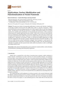
structure on a carbon surface, (4) using microcontact-printed PAS-based polyelectrolyte multilayer as a mask for wet etching, and (5) producing highly engineered microparticles (Figure 1).
Figure 1. Schematic representation of versatile surface micropatterning and functionalization enabled by μCP of PAS.
2. EXPERIMENTAL SECTION Materials. PAS was purchased from Polysciences Inc. [molecular weight (MW): >150 000 g/mol]. HiPco single-walled carbon nanotubes (SWCNTs) were purchased from Unidym Inc (Sunnyvale, CA). Highly ordered pyrolytic graphite (HOPG) was purchased from SPI Supplies (West Chester, PA). Potassium iodide-based standard Received: August 25, 2014 Revised: October 18, 2014 Published: October 22, 2014 13483
dx.doi.org/10.1021/la503393j | Langmuir 2014, 30, 13483−13490
Langmuir
Article
Figure 2. Micropatterning biomolecules and nanomaterials with microcontact-printed PAS. (A1) Fluorescence micrograph of micropatterned DNA (YOYO-1-stained, green). Diazotization time: 20 min. (A2) Plot of fluorescence intensity of micropatterned DNA against diazotization time. (B) Fluorescence micrograph of comicropatterned lateral avidin stripes stained by fluorescein−biotin (green) and vertical DNA stripes stained by PI (red). (C1) Height AFM image of SWCNTs immobilized on diazotized PAS stripes. Inset shows a magnified region of the micropatterned SWCNTs. (C2) Raman spectra of the micropatterned SWCNTs (red) and the pristine SWCNTs (blue). The spectra were normalized against the peak intensities of the G bands. (D1) Height AFM image of 14 nm diameter AuNPs immobilized on diazotized PAS stripes printed on a glass slide. Inset shows a magnified region of the micropatterned AuNPs. (D2) Height profile of the line segment in (B1). (D3) UV−vis spectrum of the micropatterned AuNPs. slide and kept at 4 °C for 2 h, followed by washing the slide with ethanol and water consecutively. Micropatterning Gold Nanoparticles (AuNPs). AuNPs with a mean hydrodynamic diameter of 14.0 nm were synthesized as described in ref 31. The pH of the as-synthesized water suspension of AuNPs was adjusted to 7. PAS stripes were printed on a plasmatreated glass slide and diazotized as described above. The suspension of AuNPs (1 mL, precooled at 0 °C) was added on the slide and kept at 4 °C for 2 h, followed by washing the slide with ethanol and water consecutively. μCP of a Metallic Structure on HOPG. A 10 nm thick gold film was sputter-coated on a microridge stamp. A featureless flat PDMS stamp was coated with a monolayer of PAS with the same procedure for inking the micropillar stamp as above. The flat stamp was brought into contact with the gold-coated microridge stamp and kept for 1 min, followed by separating the stamps. Diazotization was carried out by placing the microridge stamp above an ice-cold acidified nitrite solution (15 mL; nitrite concentration: 1 mM; HCl concentration: 0.5 M) for 30 min. Then the stamp was brought into contact with a freshly cleaved HOPG precooled on ice. A pressure (300 g/cm2) was applied on the stamp and maintained for 30 min followed by peeling the stamp off. The second array of gold stripes perpendicular to the first array was printed following the same procedure. Using Microcontact-Printed PAS-Based Multilayer as an Etch Mask. μCP of the PAS/poly(sodium 4-styrenesulfonate) (PSS)/ PAS trilayer micropads was performed by soaking a micropillar stamp in a PAS solution (0.5 wt %, pH 4, 10 min), then a PSS solution (0.5 wt %, pH 4, 10 min), and finally the PAS solution again (10 min). Each soaking was followed by a brief wash of the stamp with water, and the final wash was followed by drying the stamp with a nitrogen stream. Next, the stamp was placed on a glass slide coated with a 20 nm thick gold film on a 5 nm thick titanium film deposited with a thermal evaporator. The contact was maintained for 1 min, followed by peeling the stamp off. Etching was performed by covering the printed area with the etchant (diluted 50 times with water, 1 mL) for 20 min. After that, the slide was washed with water. Poly(allylamine hydrochloride) (PAH)-based trilayer was printed and tested as described above, except using solutions of PAH (0.5 wt %, pH 7) and PSS (0.5 wt %, pH 6).
gold etchant and DNA of salmon testis were purchased from SigmaAldrich. PDMS (Sylgard 184) stamps with two types of surface features were used here: (1) 7 μm diameter circular pillars in a square lattice with 20 μm in center-to-center distance and 3.4 μm in height and (2) ∼1.6 μm wide straight ridges with 4 μm in pitch and 1.2 μm in height. μCP of PAS. A stamp was inked by immersing the stamp in a PAS solution (0.5 wt %, pH 4, containing ∼100 mM NaCl) for 10 min and then rinsed with water and dried with a nitrogen stream. Printing was performed by placing the PAS-inked stamp on a substrate, maintaining the contact for 1 min, and finally peeling the stamp off the substrate. Micropatterning DNA. Circular PAS micropads were printed on a poly(ethylene glycol) (PEG)-silane-coated glass slide, which was prepared as described in ref 28. The microcontact-printed PAS stripes were diazotized by immersing the slide in a nitrite solution (1 mg/mL) acidified by HCl (0.5 M) at 0 °C for a series of durations. After briefly washing the glass slide with ice-cold water, an ice-cold solution of YOYO-1-stained DNA (0.1 mg/mL, 100 μL, dye-to-base pair ratio = 1:30) in water was immediately added on the slide and kept in a cold room (4 °C) for 30 min. Finally, the slide was washed with water. Comicropatterning Avidin and DNA. PAS stripes were printed on a PEG-silane-coated glass slide and diazotized by immersing the slide in a nitrite solution (1 mg/mL) acidified by HCl (0.5 M) at 0 °C for 30 min. After briefly washing the slide with ice-cold water, an icecold avidin solution (1 mg/mL, 100 μL) was immediately added on the stripes and kept at 4 °C for 2 h. Next, the slide was briefly washed with water and dried with a nitrogen stream. A stamp with the same feature was then used to print a second array of PAS stripes perpendicular to the avidin stripes. The second array of PAS stripes were diazotized as above and used to immobilize unstained DNA (0.1 mg/mL, 100 μL, 1 h incubation). After washing the slide with water, a solution (300 μL) of biotin−fluorescein (1 mg/mL) and PI (50 μg/ mL) was added on the stripes and kept at 4 °C for 1 h, followed by a wash with water. Micropatterning SWCNTs. The SWCNT dispersion was prepared as described in refs 29 and 30. PAS stripes were printed on a plasma-treated glass slide and diazotized as described above. An ice-cold water dispersion of SWCNTs (1 mL) was then added on the 13484
dx.doi.org/10.1021/la503393j | Langmuir 2014, 30, 13483−13490
Langmuir
Article
Producing Highly Engineered Microparticles. A (PAS/PSS)2/ PAS multilayer was assembled on a micropillar stamp with the same method as for preparing the PAS/PSS/PAS trilayer. A 10 nm thick gold film was sputter-coated on the stamp, which was then brought into contact with a poly(vinyl alcohol) (PVA)-coated glass slide and kept for 1 min. Diazotization was carried out as described the section “μCP of a Metallic Structure on HOPG”. Release and functionalization of the microparticles were done by adding bovine serum albumin (BSA)−rhodamine B isothiocyanate (RITC) solution (500 μL, 25 μg/ mL) on the slide and incubated for 3 h at 0 °C. Characterization. Atomic force microscopy (AFM) images were obtained using a Bruker Dimension Icon operated at tapping mode in air. Raman spectra were obtained using a Jobin-Yvon Horiba LabRAM HR800 spectrometer equipped with a 785 nm diode laser.
a significant effect on the amount of immobilized DNA. To examine this point, the degree of diazotization was varied by soaking the PAS micropads to the acidified nitrite solution for different time durations, and its effect on the amount of immobilized DNA was studied. Figure S3B shows the result. Figure 2A2 summarizes the averaged fluorescence intensity per micropad versus soaking time. As expected, with increasing the soaking time, the fluorescence intensity and therefore the amount of immobilized DNA showed a monotonic increase initially and then reached saturation at the soaking time of ∼20 min. The saturation plateau indicates the kinetic equilibrium of diazotization reaction being reached. It is of note that the DNA used here was double-stranded, and immobilized doublestranded DNA has been used to prepare DNA microarrays.33 Besides DNA, we comicropatterned DNA and avidin as follows. First, PAS stripes with a lateral orientation were printed on a PEG-silane-coated glass slide and then diazotized and used to immobilize avidin. Next, vertical PAS stripes were printed on the same area and diazotized and used to immobilize unstained DNA. To visualize the immobilized DNA and avidin, the patterned area was exposed to a mixture of propidium iodide (PI) and biotin−fluorescein conjugate in water. Note that PI is a DNA dye, and biotin−fluorescein specifically stains functioning avidin. Figure 2B shows green lateral stripes (characteristic emission of biotin−fluorescein) and red vertical stripes (characteristic emission of PI dye), proving that DNA and avidin can be comicropatterned by this method. It should be emphasized that the ability of avidin to bind to biotin was not adversely affected by the immobilization of avidin and the second diazotization step. Micropatterning of nanomaterials is necessary for fabricating many useful devices such as SWCNTs for building flexible integrated circuits and AuNPs for preparing biosensors.34,35 We micropatterned these two types of nanomaterials using microcontact-printed PAS stripes by incubating the diazotized PAS stripes in water dispersion of SWCNTs and AuNPs, respectively. AFM characterization of the micropatterned SWCNTs reveals an entangled network of one-dimensional nanostructures (Figure 2C1). The Raman spectrum further confirms the presence of SWCNTs on the PAS stripes (Figure 2C2). It is noted that the micropatterned SWCNTs exhibited a significantly lower intensity ratio of the G band to D band (IG/ ID = 4.2) than that of pristine SWCNTs (IG/ID = 16.9). Since SWCNTs can be chemically grafted with aryldiazonium salts and the reaction leads to a reduction in IG/ID,10 the immobilization of the SWCNTs on the diazotized PAS stripes and the decreased IG/ID of the micropatterned SWCNTs can probably be attributed to the formation of chemical bonds between the SWCNTs and the diazotized PAS. Figures 2D1 and 2D2 show micropatterned AuNPs. The successful immobilization of AuNPs on the PAS stripes was further confirmed by the UV−vis spectrum (Figure 2D3), which reveals the surface plasmon resonance (SPR) peak of gold nanoparticles at 530 nm. This value is slightly greater than 519 nmthe SPR peak of the as-synthesized suspension of AuNPs (Figure S4). The red-shift indicates that the immobilized AuNPs were closely packed.36 Enabling μCP of a Metallic Structure on a Carbon Surface. Micro/nanopatterned metallic structures are essential components of many devices including integrated circuits. On the other hand, graphene promises to be a revolutionary functional material for diverse applications. We envision that a simple, low-cost, and environment-friendly method allowing
3. RESULTS AND DISCUSSION μCP of PAS. Micropatterning of biomolecules and nanomaterials relies on μCP and diazotization of PAS. We thus first studied μCP of PAS. An aqueous solution of PAS with pH set at 4 was prepared for μCP of PAS. The brownish and clear PAS solution (Figure S1A) showed a strong absorbance peak at 430 nm in the visible spectrum (Figure S1B). The same solution had a fluorescent emission peak at 540 nm under 430 nm excitation (Figure S1C). The procedure for μCP of PAS included four steps: (1) soaking an unmodified PDMS stamp in the aqueous solution of PAS, (2) rinsing the stamp with water and drying the stamp with a stream of nitrogen, (3) bringing the stamp into contact with a substrate, and (4) peeling the stamp off the substrate. By taking advantage of the autofluorescence of PAS, we used fluorescence microscopy to examine the printed PAS microstructures. Figure S2A shows the pad-like PAS microstructures (termed micropads hereafter) on a glass slide. The fluorescence intensities of individual micropads were uniform across the entire printing area. Measurement of fluorescence intensities of 258 micropads reveals a Gaussian distribution (Figure S2B). The micropads were further characterized with AFM. Figure S2C shows the representative result. The micropads all displayed smooth surface and showed the same shape and lateral size as the micropillars of the stamp. A thickness measurement gave 2.3 ± 0.3 nm (mean ± standard deviation, n = 12), suggesting that a monolayer of PAS was adsorbed to the stamp surface as in μCP of PAH.5,32 Micropatterning Biomolecules and Nanomaterials. Micropatterning of biomolecules is essential to various techniques and assays for biomedical sensing and analysis. We chose DNA and a proteinavidinto demonstrate the capability of our technique for micropatterning biomolecules. To micropattern DNA, the microcontact-printed PAS micropads were first diazotized by soaking the micropads in an acidified nitrite solution.27 The diazotized PAS micropads were then incubated in a solution of YOYO-1-stained DNA. Figure 2A1 shows a portion of a centimeter wide array of micropatterned DNA. Note that, under the same imaging conditions, the fluorescence of the diazotized micropads immobilized by DNA shown in Figure 2A1 was much brighter than that of the pristine PAS micropads (Figure S3A). This indicates that the bright fluorescence of the micropads in Figure 2A1 was mainly due to the YOYO-1-stained DNA and the contribution of the autofluorescence of PAS was negligible. Presumably, the covalent bonding between DNA and the aryldiazonium salt was responsible for the immobilization of DNA on the diazotized PAS micropads. As a consequence, the degree of diazotization of the pristine PAS was expected to have 13485
dx.doi.org/10.1021/la503393j | Langmuir 2014, 30, 13483−13490
Langmuir
Article
Figure 3. Enabling μCP of a metallic structure on a carbon surface. (A) Schematic of fabrication procedure. (B) Fluorescence micrograph of the flat PDMS stamp coated with PAS after contacting the microridge PDMS stamp coated with Au film. (C) Scanning electron micrograph of the Au crossbar on HOPG. (D) EDX spectra of the Au crossbar on HOPG. (E) Height AFM image of the Au crossbar on HOPG. (F) Height profile of the line segment in (E).
crossbars,38,39 but our method is featured by an ability to print metallic structures on HOPG and probably on graphene. Using Microcontact-Printed PAS-Based Polyelectrolyte Multilayer as a Mask for Wet Etching. Wet etching is used extensively in the microelectronics industry for manufacturing integrated circuits. Self-assembled monolayers (SAMs) of small molecules patterned by μCP have been explored as etch masks.40,41 Nevertheless, this type of mask is prone to pinhole defects due to the extremely small thickness of the SAMs. Such a problem can be alleviated by grafting a polymer-based multilayer on microcontact-printed SAM of alkanethiolate,42 but there is still a resolution issue limited by the high diffusivity of the small-molecule inks.43 In contrast, the microcontact-printed polyelectrolyte-based multilayer can have a much greater thickness and presumably a much lower pinhole density than the small-molecule SAMs. The high molecular weights of the polyelectrolytes and the strong electrostatic attraction between the polycation and polyanion also make the diffusivity of the multilayer ink much lower than that of the small-molecule inks. Lastly, given pKa of 4.63 for the conjugate acid of aniline,44 PAS is expected to be positively charged at pH 4, therefore allowing building a multilayer with a polyanion such as PSS through LbL assembly. Also given the hydrophobic nature of benzene ring and unprotonated primary amine,45,46 PAS is expected to be highly hydrophobic at pH 7, thus rendering the PAS-based multilayer impermeable to waterbased etchants at this pH. We examined the hydrophobic nature of the PAS-based multilayer by printing a featureless PAS/PSS/PAS trilayer film on a plasma-treated glass slide with a flat PDMS stamp. To qualitatively assess the hydrophobicity of the film, we soaked the slide in water for 30 min and then pulled it out. An instantaneous dewetting of water from the PAS/PSS/PAS-coated slide was observed, which suggests the PAS/PSS/PAS film was hydrophobic. In contrast, a similarly printed PAH/PSS/PAH film retained a thin layer of water film upon the same soaking and pulling-out process. Note that with the pKa of 8.8 for the conjugate acid of PAH,47 PAH should be highly charged at pH 7. The hydrophobic nature of the PAS/ PSS/PAS film was also quantitatively confirmed by the 93°
printing metallic micro/nanostructures on graphene would open up myriad opportunities for practical applications. By taking advantage of the ability of the diazotized PAS to covalently bond to both metals and carbons, we demonstrate μCP of a gold crossbara model metallic micro/nanostructure on HOPGa multilayer of graphene.37 The fabrication process is schematically shown in Figure 3A and briefly described as follows. (1) A monolayer of PAS was adsorbed on a featureless flat PDMS stamp by soaking the stamp in the aqueous PAS solution. A 10 nm thick gold film was sputter-coated on a second PDMS stamp bearing straight microridges. (2) Subtraction printing was performed between the two stamps to transfer the PAS layer from the flat stamp on to the top surface of the gold-coated microridges. Successful transfer was confirmed by the stripe pattern of the PAS monolayer left on the flat stamp (Figure 3B). (3) The microridge stamp was then exposed to vapor generated from the acidified nitrite solution to diazotize PAS.27 (4) The stamp was brought into contact with a freshly cleaved HOPG surface, resulting in transfer of the PAS monolayer together with the gold film atop the microridges to form the printed stripes on the HOPG surface. (5) By repeating the above procedure, a second array of stripes was printed perpendicular to the previously formed one to generate a crossbar on the HOPG surface. The crossbar covered the entire printing area with a representative portion shown in Figure 3C. Energy-dispersive X-ray (EDX) spectroscopy (Figure 3D) confirmed the chemical compositions of the crossbar (gold) and the underlying HOPG (carbon). The crossbar structure was also imaged by AFM (Figure 2E), and the height of the Au/PAS stripes was measured as ∼11.0 nm (Figure 3F). It should be emphasized that the diazotized PAS played an essential role for the successful μCP of the gold crossbar on HOPG. To prove this point, we attempted to transfer gold film to HOPG surface without PAS or with pristine PAS. In both cases, the gold film was not transferred (Figure S5A,B). This result suggests that the covalent bonding between aryldiazonium salt and HOPG and gold was responsible for gluing these two dissimilar materials together. It is of note that μCP has been used to fabricate metallic 13486
dx.doi.org/10.1021/la503393j | Langmuir 2014, 30, 13483−13490
Langmuir
Article
Figure 4. Using PAS-based polyelectrolyte multilayer as an etch mask. (A) Schematic of experimental procedure. (B) Height AFM image of PAS/ PSS/PAS micropads printed on a glass slide coated with a gold (thickness: 20 nm)/titanium film. (C) Height profile of the line segment in (B). (D) Height AFM image of the sample after etching. (E) Height profile of the line segment in (D). (F) Bright-field optical micrograph of the sample after etching.
Figure 5. Producing highly engineered microparticles. (A) Schematic of fabrication procedure. (B) Height AFM image of (PAS/PSS)2/PAS/Au microparticles printed on a glass slide coated with a SAM of thiol−silane. (C) Height profile of the line segment in (C). (D) Bright-field optical micrograph of (PAS/PSS)2/PAS/Au microparticles printed on a PVA-coated glass slide. (E) Overlaid fluorescence and bright-field micrograph of released (PAS/PSS)2/PAS/Au microparticles functionalized with BSA-RITC (red).
stationary contact angle of water on the PAS/PSS/PAS-coated slide measured immediately after pulling the slide out of water (Figure S6A). After establishing the hydrophobic nature of PAS/PSS/PAS film, we used the microcontact-printed PASbased trilayer as the etch mask to micropattern a gold film as schematically shown in Figure 4A. In brief, an array of 7 μm diameter micropads made of PAS/PSS/PAS trilayer was printed on a glass slide, which was coated by a 20 nm thick gold film with a 5 nm thick titanium film as the adhesion layer. The micropads had a thickness of ∼6.1 nm (Figure 4B,C). The slide was incubated in a diluted commercial KI/I2 gold etchant (pH 7) for 20 min, resulting in generation of an array of ∼26 nm thick disks (Figure 4D,E), indicating etching away of uncovered gold and retention of gold under the PAS/PSS/PAS
micropads. The successful use of the PAS-based mask was confirmed by the bright-field optical micrograph (Figure 4F). The importance of PAS in the mask was further proved by a contrast experiment, in which PAH/PSS/PAH trilayer micropads were used as a mask (Figure S6B). With the same etching conditions as above applied, the entire gold film was etched away (Figure S6C), indicating that the PAH/PSS/PAH micropads failed to protect the underlying gold film. Producing Highly Engineered Microparticles. Microparticles are widely studied for various biomedical applications such as drug delivery and biomolecule analysis. Top-down fabrication technology allows producing highly engineered microparticles with tightly controlled compositions, structures, and properties that cannot be achieved by the bottom-up 13487
dx.doi.org/10.1021/la503393j | Langmuir 2014, 30, 13483−13490
Langmuir
Article
methods.48−52 We previously developed a μCP-based technique to produce microparticles composed of multilayered polyelectrolytes.53 Here we integrate this technique with μCP of PAS and aryldiazonium chemistry to produce microparticles with an unprecedented metal−polyelectrolytes−protein structure. The fabrication procedure is illustrated in Figure 5A. In brief, a five-layer (PAS/PSS)2/PAS film was first coated onto a PDMS stamp bearing the 7 μm diameter circular pillars. A gold (Au) film of 10 nm thick was then sputter-coated on the stamp. Next, the (PAS/PSS)2/PAS/Au multilayer structure on the top of the micropillars was transferred on to a glass slide coated with a thin film of PVA. The PAS of the multilayer was diazotized upon exposure to vapor of an acidified nitrite solution. An aqueous solution of BSA labeled with RITC was added onto the slide to release the microparticles by dissolving the PVA film and to functionalize the microparticles with the protein through the acryldiazonium-based coupling reaction. The final product is a batch of microparticles composed a gold film, a (PAS/PSS)2/PAS multilayer, and surface-grafted BSARITC. To characterize the morphology and dimensions of the microparticles, we printed the (PAS/PSS)2/PAS/Au microparticles on to a glass slide coated with a SAM of 3mercaptopropyltrimethoxysilane (MPTMS). The use of MPTMS was to facilitate the transfer through forming the gold−thiol bonding. AFM image (Figure 5B) reveals uniform dimensions of the transferred (PAS/PSS)2/PAS/Au microparticles in both lateral and vertical directions. The thickness of the (PAS/PSS)2/PAS/Au structure (Figure 5C) was determined to be ∼17.0 nm. Considering the gold film of 10.0 nm in thickness, we can estimate the five-layer (PAS/PSS)2/PAS has a thickness of ∼7.0 nm. The successful transfer of the (PAS/ PSS)2/PAS/Au structures to the PVA-coated slide over the entire printing area was confirmed by bright-field optical microscopy (Figure 5D). An inverted fluorescence microscope was used to examine the released microparticles functionalized with BSA-RITC with green light as the excitation source. The result is shown in Figure 5E. Interestingly, not all the microparticles emitted red lightthe characteristic color of rhodamine-B-labeled BSA. Instead, a good portion of the microparticles appeared black. We believe that the difference of the color appearance of the microparticles was caused by their facing direction with respect to the excitation source. When the Au side of the microparticle facing toward the excitation source, both excitation and emission light experienced strong absorption to cause the dark appearance. This absorption was not a problem for the microparticles with the Au side facing away from the excitation source. In such a case, the microparticles emitted the characteristic color of rhodamine B and appeared red. A shape change from the original circular to polygonal was noticed for the released microparticles due to folding of the edges of the microparticles. It should be noted that μCP with the unmodified PDMS stamp has been used to print thin-film metallic microstructures based on depositing the metal directly on an unmodified PDMS stamp.54 In contrast, our method features use of a PAS-based polyelectrolyte multilayer to separate the metal layer and the stamp surface. As a consequence, there is no residual metal left on the stamp after printing, which makes the stamp cleaning an easy task. This is particularly desirable for repeated use of the stamp in an envisioned industrial setting. Moreover, our method allows facile fabrication of the layered asymmetrical Au−polyelectrolyte hybrid microparticles, which have never
been reported before. Besides gold, our method is, in principle, applicable to other metals or alloys such as permalloy, which can render the microparticles magnetically active.55 Our method is also featured by an ability to functionalize the microparticles with various biomolecules and nanomaterials through the aryldiazonium chemistry. For example, by replacing BSA-RITC with another protein such as an antibody in our method, microparticles with targeting ability can be produced.55
4. CONCLUSION PAS can be microcontact-printed as a monolayer or a polyelectrolyte multilayer using an unmodified PDMS stamp and water as the ink solvent. The microcontact-printed PAS can be diazotized to covalently micropattern various technologically important materials including DNA, proteins, SWCNTs, and AuNPs. The diazotized PAS enables μCP of thin-film gold microstructures on HOPG and likely on graphene. Moreover, the hydrophobic nature of PAS at the neutral pH allows the microcontact-printed PAS-based polyelectrolyte multilayer being used as a mask for wet etching. In addition, highly engineered microparticles can be prepared by combining μCP and diazotization of PAS. Overall, this work has established a novel μCP platform technique that is inexpensive, simple, and featured by the use of a single ink material to enable highly versatile surface micropatterning and functionalization with various potential applications.
■
ASSOCIATED CONTENT
S Supporting Information *
Figures S1−S6. This material is available free of charge via the Internet at http://pubs.acs.org.
■
AUTHOR INFORMATION
Corresponding Author
*E-mail
[email protected]; Tel 18504106643; Fax 18504106150 (J.G.). Notes
The authors declare no competing financial interest.
■
ACKNOWLEDGMENTS This study was funded by United States National Science Foundation Award 1300447. We thank Drs. Daniel Gallego Perez and Derek Hansford of the Department of Biomedical Engineering at The Ohio State University for assistance on stamp preparation, Drs. Peng Xiong and Eric Lochner of Department of Physics at Florida State University (FSU) for assistance on the preparation of Au/Ti-coated glass slides, and Dr. Joseph Schlenoff of Department of Chemistry and Biochemistry at FSU for assistance on the contact angle measurement.
■
REFERENCES
(1) Quist, A. P.; Pavlovic, E.; Oscarsson, S. Recent advances in microcontact printing. Anal. Bioanal. Chem. 2005, 381, 591−600. (2) Ruiz, S. A.; Chen, C. S. Microcontact printing: A tool to pattern. Soft Matter 2007, 3, 168−177. (3) Kaufmann, T.; Ravoo, B. J. Stamps, inks and substrates: polymers in microcontact printing. Polym. Chem. 2010, 1, 371−387. (4) Park, J.; Kim, Y. S.; Hammond, P. T. Chemically nanopatterned surfaces using polyelectrolytes and ultraviolet-cured hard molds. Nano Lett. 2005, 5, 1347−1350.
13488
dx.doi.org/10.1021/la503393j | Langmuir 2014, 30, 13483−13490
Langmuir
Article
(5) Park, J.; Hammond, P. T. Multilayer transfer printing for polyelectrolyte multilayer patterning: direct transfer of layer-by-layer assembled micropatterned thin films. Adv. Mater. 2004, 16, 520−525. (6) Wang, Z.; Xia, J.; Guan, J. Micro/Nanocontact printing of watersoluble biomacromolecules and polymers. ScienceJet 2014, 3, 58. (7) Mangeney, C.; Qin, Z.; Dahoumane, S. A.; Adenier, A.; Herbst, F.; Boudou, J. P.; Pinson, J.; Chehimi, M. M. Electroless ultrasonic functionalization of diamond nanoparticles using aryl diazonium salts. Diamond Relat. Mater. 2008, 17, 1881−1887. (8) Abiman, P.; Wildgoose, G. G.; Compton, R. G. A mechanistic investigation into the covalent chemical derivatisation of graphite and glassy carbon surfaces using aryldiazonium salts. J. Phys. Org. Chem. 2008, 21, 433−439. (9) Chen, H.; Wang, Y.; Qu, J.; Dong, S. Self-assembled silver nanoparticle monolayer on glassy carbon: an approach to SERS substrate. J. Raman Spectrosc. 2007, 38, 1444−1448. (10) Bahr, J. L.; Yang, J.; Kosynkin, D. V.; Bronikowski, M. J.; Smalley, R. E.; Tour, J. M. Functionalization of carbon nanotubes by electrochemical reduction of aryl diazonium salts: a bucky paper electrode. J. Am. Chem. Soc. 2001, 123, 6536−6542. (11) Wang, Q.; Jin, Z.; K. Kim, K.; Hilmer, A. J.; Paulus, G. L. C.; Shih, C. J.; Ham, M. H.; Sanchez-Yamagishi, J. D.; Watanabe, K.; Taniguchi, T.; Kong, J.; Jarillo-Herrero, P.; Strano, M. S. Understanding and controlling the substrate effect on graphene electrontransfer chemistry via reactivity imprint lithography. Nat. Chem. 2012, 4, 724−732. (12) Gehan, H.; Fillaud, L.; Felidj, N.; Aubard, J.; Lang, P.; Chehimi, M. M.; Mangeney, C. A general approach combining diazonium salts and click chemistries for gold surface functionalization by nanoparticle assemblies. Langmuir 2010, 26, 3975−3980. (13) Combellas, C.; Delamar, M.; Kanoufi, F.; Pinson, J.; Podvorica, F. I. Spontaneous grafting of iron surfaces by reduction of aryldiazonium salts in acidic or neutral aqueous solution. Application to the protection of iron against corrosion. Chem. Mater. 2005, 17, 3968−3980. (14) Lehr, J. Patterning of metal, carbon, and semiconductor substrates with thin organic films by microcontact printing with aryldiazonium salt inks. Anal. Chem. 2010, 82, 7027−7034. (15) Iruthayaraj, J.; Chernyy, S.; Lillethorup, M.; Ceccato, M.; Røn, T.; Hinge, M.; Kingshott, P.; Besenbacher, F.; Pedersen, S. U.; Daasbjerg, K. On surface-initiated atom transfer radical polymerization using diazonium chemistry to introduce the initiator layer. Langmuir 2011, 27, 1070−1078. (16) Le, X. T.; Zeb, G.; Jegou, P.; Berthelot, T. Electrografting of stainless steel by the diazonium salt of 4-aminobenzylphosphonic acid. Electrochim. Acta 2012, 71, 66−72. (17) Flavel, B. S.; Gross, A. J.; Garrett, D. J.; Nock, V.; Downard, A. J. A simple approach to patterned protein immobilization on silicon via electrografting from diazonium salt solutions. ACS Appl. Mater. Interfaces 2010, 2, 1184−1190. (18) Hadj, F. A. E.; Amiar, A.; Cherkaoui, M.; Chazalviel, J. N.; Ozanam, F. Study of organic grafting of the silicon surface from 4nitrobenzene diazonium tetrafluoroborate. Electrochim. Acta 2012, 70, 318−334. (19) Lefèvre, X.; Segut, O.; Jégou, P.; Palacin, S.; Jousselme, B. Towards organic film passivation of germanium wafers using diazonium salts: Mechanism and ambient stability. Chem. Sci. 2012, 3, 1662−1671. (20) Rawson, F. J.; Yeung, C. L.; Jackson, S. K.; Mendes, P. M. Tailoring 3D single-walled carbon nanotubes anchored to indium tin oxide for natural cellular uptake and intracellular sensing. Nano Lett. 2012, 13, 1−8. (21) Howard, A. N.; Wild, F. The reactions of diazonium compounds with amino acids and proteins. Biochem. J. 1957, 65, 651−659. (22) Berthelot, T.; Garcia, A.; Le, X. T.; El Morsli, J.; Jégou, P.; Palacin, S.; Vielb, P. Ultrasensitive detection of adrenocorticotropin hormone (ACTH) using disposable phenylboronic-modified electrochemical immunosensors. Appl. Surf. Sci. 2011, 257, 3538−3546.
(23) Moreno-Guzmán, M.; Ojeda, I.; Villalonga, R.; González-Cortés, A.; Yáñez-Sedeño, P.; Pingarrón, J. M. Versatile toolset” for DNA or protein immobilization: toward a single-step chemistry. Biosens. Bioelectron. 2012, 35, 82−86. (24) Dolan, P. L.; Wu, Y.; Ista, L. K.; Metzenberg, R. L.; Nelson, M. A.; Lopez, G. P. Robust and efficient synthetic method for forming DNA microarrays. Nucleic Acids Res. 2001, 29, E107. (25) Boland, S.; Barrière, F.; Leech, D. Designing stable redox-active surfaces: chemical attachment of an osmium complex to glassy carbon electrodes prefunctionalized by electrochemical reduction of an in situgenerated aryldiazonium cation. Langmuir 2008, 24, 6351−6358. (26) Garrett, D. J.; Lehr, J.; Miskelly, G. M.; Downard, A. J. Microcontact printing using the spontaneous reduction of aryldiazonium salts. J. Am. Chem. Soc. 2007, 129, 15456−15457. (27) Wang, Z.; Wang, J.; Xiao, Z.; Xia, J.; Zhang, P.; Liu, T.; Guan, J. A paper indicator for triple-modality sensing of nitrite based on colorimetric assay, Raman spectroscopy, and electron paramagnetic resonance spectroscopy. Analyst 2013, 138, 7303−730. (28) Wang, Z.; Zhang, P.; Kirkland, B.; Liu, Y.; Guan, J. Microcontact printing of polyelectrolytes on PEG using an unmodified PDMS stamp for micropatterning nanoparticles, DNA, proteins and cells. Soft Matter 2012, 8, 7630−7637. (29) Liu, T.; Luo, S.; Xiao, Z.; Zhang, C.; Wang, B. Preparative ultracentrifuge method for characterization of carbon nanotube dispersions. J. Phys. Chem. C 2008, 112, 19193−19202. (30) Liu, T.; Xiao, Z.; Wang, B. The exfoliation of SWCNT bundles examined by simultaneous Raman scattering and photoluminescence spectroscopy. Carbon 2009, 47, 3529−3537. (31) Jana, N. R.; Gearheart, L.; Murphy, C. J. Evidence for seedmediated nucleation in the chemical reduction of gold salts to gold nanoparticles. Chem. Mater. 2001, 13, 2313−2322. (32) Berg, M. C.; Choi, J.; Hammond, P. T.; Rubner, M. F. Tailored micropatterns through weak polyelectrolyte stamping. Langmuir 2003, 19, 2231−2237. (33) Miller, M. B.; Tang, Y.-W. Basic Concepts of microarrays and potential applications in clinical microbiology. Clin. Microbiol. Rev. 2009, 22, 611−633. (34) Cao, Q.; Kim, H. S.; Pimparkar, N.; Kulkarni, J. P.; Wang, C.; Shim, M.; Roy, K.; Alam, M. A.; Rogers, J. A. Medium-scale carbon nanotube thin-film integrated circuits on flexible plastic substrates. Nature 2008, 454, 495−500. (35) Park, S. J.; Taton, T. A.; Mirkin, C. A. Array-based electrical detection of DNA with nanoparticle probes. Science 2002, 295, 1503− 1506. (36) Brust, M.; Bethell, D.; Kiely, C. J.; Schiffrin, D. J. Self-Assembled gold nanoparticle thin film with nonmetallic optical and electronic properties. Langmuir 1998, 14, 5425−5429. (37) Novoselov, K. S.; Geim, A. K.; Morozov, S. V.; Jiang, D.; Zhang, Y.; Dubonos, S. V.; Grigoreva, I. V.; Firsov, A. A. Electric field effect in atomically thin carbon films. Science 2004, 306, 666−669. (38) Stuart, C.; Park, H. K.; Chen, Y. Fabrication of a 3D nanoscale crossbar circuit by nanotransfer-printing lithography. Small 2010, 6, 1663−1668. (39) Sanetra, N.; Karipidou, Z.; Wirtz, R.; Knorr, N.; Rosselli, S.; Nelles, G.; Offenhaeusser, A.; Mayer, D. Printing of highly integrated crossbar junctions. Adv. Funct. Mater. 2012, 22, 1129−1135. (40) Xia, Y.; Zhao, X. M.; Whitesides, G. M. Pattern transfer: Selfassembled monolayers as ultrathin resists. Microelectron. Eng. 1996, 32, 255−268. (41) Love, J. C.; Wolfe, D. B.; Chabinyc, M. L.; Paul, K. E.; Whitesides, G. M. Self-assembled monolayers of alkanethiolates on palladium are good etch resists. J. Am. Chem. Soc. 2002, 124, 1576− 1577. (42) Huck, W. T. S.; Yan, L.; Stroock, A.; Haag, R.; Whitesides, G. M. Patterned polymer multilayers as etch resists. Langmuir 1999, 15, 6862−6867. (43) Xia, Y.; Whitesides, G. M. Use of controlled reactive spreading of liquid alkanethiol on the surface of gold to modify the size of 13489
dx.doi.org/10.1021/la503393j | Langmuir 2014, 30, 13483−13490
Langmuir
Article
features produced by microcontact printing. J. Am. Chem. Soc. 1995, 117, 3274−3275. (44) Hornback, J. M. In Organic Chemistry, 2nd ed.; McMurry, J. E., Ed.; Cengage Learning: Stamford, CT, 2005. (45) Vezenov, D. V.; Noy, A.; Rozsnyai, L. F.; Lieber, C. M. Force titrations and ionization state sensitive imaging of functional groups in aqueous solutions by chemical force microscopy. J. Am. Chem. Soc. 1997, 119, 2006−2015. (46) Zhang, H.; He, H. X.; Wang, J.; Mu, T.; Liu, Z. F. Force titration of amino group-terminated self-assembled monolayers using chemical force microscopy. Appl. Phys. A: Mater. Sci. Process. 1998, 66, S269− S271. (47) Choi, J.; Rubner, M. F. Influence of the degree of ionization on weak polyelectrolyte multilayer assembly. Macromolecules 2005, 38, 116−124. (48) Ahmed, A.; Bonner, C.; Desai, T. A. Bioadhesive microdevices for drug delivery: a feasibility study. Biomed. Microdevices 2011, 3, 89− 96. (49) Guan, J.; He, H.; Lee, L. J.; Hansford, D. J. Fabrication of particulate reservoir-containing, capsulelike, and self-folding polymer microstructures for drug delivery. Small 2007, 3, 412−418. (50) Pregibon, D. C.; Toner, M.; Doyle, P. S. Multifunctional encoded particles for high-throughput biomolecule analysis. Science 2007, 315, 1393−1396. (51) Decuzzi, P.; Pasqualini, R.; Arap, W.; Ferrari, M. Intravascular delivery of particulate systems: Does geometry really matter? Pharm. Res. 2009, 26, 235−243. (52) Perry, J. L.; Herlihy, K. P.; Napier, M. E.; Desimone, J. M. PRINT: a novel platform toward shape and size specific nanoparticle theranostics. Acc. Chem. Res. 2001, 44, 990−998. (53) Zhang, P.; Guan, J. Fabrication of multilayered microparticles by integrating layer-by-layer assembly and microcontact printing. Small 2001, 7, 2998−3004. (54) Loo, Y. L.; Lang, D. V.; Rogers, J. A.; Hsu, J. W. P. Electrical contacts to molecular layers by nanotransfer printing. Nano Lett. 2003, 3, 913−917. (55) Kim, D. H.; Rozhkova, E. A.; Ulasov, I. V.; Bader, S. D.; Rajh, T.; Lesniak, M. S.; Novosad, V. Biofunctionalized magnetic-vortex microdiscs for targeted cancer-cell destruction. Nat. Mater. 2010, 9, 165.
13490
dx.doi.org/10.1021/la503393j | Langmuir 2014, 30, 13483−13490