VLSI IMPLEMENTATION OF THE REALTIME IMAGE PROCESSING PARALLEL ARCHITECTURE GFLOPS
D. HOUZET IRIT, 118 Route de Narbonne, 31062 Toulouse France Tél: (33) 61 55 63 08 Fax: (33) 61 55 62 58 e-mail:
[email protected] Abstract - This paper presents the implementation of the processor of the Image Processing parallel architecture GFLOPS. This processor is a RISC/VLIW. The network module associated in the chip is such that it is possible to build a large architecture by the juxtaposition of as many chips as required. An evaluation of this architecture is presented at the end of this paper through the use of simulation results.
INTRODUCTION A number of parallel architectures has been proposed to meet the high computational requirement of Image Processing and Computer Vision. We have developed a programmable one-dimensional multiprocessor architecture for realtime Image Processing. The GFLOPS architecture (General Flexible Linearly Organized Parallel Structure) [1] consists of multiple identical Processing Elements (PEs) interconnected with a same number of memory banks through a one-stage interconnection network. Each PE is a RISC/VLIW processor using 4 ALUs. Thus, with a 40 Mhz clock rate, one PE leads to the computational rate of 160 Mega arithmetic or logical operations per second (MOPS). Thus the power of a configuration with 256 PEs is about 40 GOPS. A basic Image Processing application like 3*3 integer convolution is processed in real-time for video data rates up to 6.25 Mbyte/s with a single PE. Using additional PEs, a tightly coupled MIMD (multi-VLIW) based multiprocessor can be built by the juxtaposition of as many PEs as required. With current 0.8 µm technology, it is possible to integrate 4 PEs in a single chip. In a first step towards a monolithic realization, one PE with only two ALUs and the network module associated has been integrated as a 1.2 µm-CMOS ASIC in a standard cell technology. This contribution presents the VLSI Implementation of a PE suitable as a building block for a MIMD based multiprocessor system for real-time Image Processing and its evaluation.
1
THE GLOBAL ARCHITECTURE We have designed a one-dimensional SIMD/MIMD distributed memory architecture, in which the processors are linked to the various memory banks through a linearly expandable network. This network is one-dimensional and provides a direct access from each processor to a subset of memory banks. The input/output system operates in parallel with the PEs in the memory banks which are built with dual-ported memories. This work follows the SYMPATI-2 project [2] which led to the development of a SIMD Line Processor. The SYMPATI-2 Line Processor is under industrialization and will be available in january 1993. This Line Processor provides excellent results as shown through our response to Preston's Abingdon Cross benchmark. Nevertheless, an attempt was made to improve this architecture whilst still keeping the idea of the one-dimensional structure of SYMPATI-2 [3],[4]. The aim of the GFLOPS architecture is to be compatible with the different levels of Image Processing. A solution is to use different stages to the different levels like the IUA project [5]. We have chosen to define a single structure which can operate in different modes. MIMD controlling of this architecture is recommended to obtain a high performance for high level algorithms, or for data dependent tasks such as blockmatching for the estimation of motion vectors from subsequent frames. To operate in MIMD mode, a memory conflict management system has been integrated in the network, in order to validate or invalidate simultaneous access requests from different PEs to a same memory bank. Also for low level regular algorithms, the processors can be synchronized to function as a large SIMD architecture. Such a double mode has been used in several projects such as PASM [6]. The synchronization of the GFLOPS architecture is managed at instruction level with a WAIT instruction using a wired-OR of synchronization flags. With the use of a global clock and one-cycle length instructions, it is thus possible to synchronize all the PEs by software at the compile time. It is possible to change from one mode to the other with the use of the synchronization flags. Also, each PE can have access to different directly accessible memory banks, one after the other, without any overhead. In addition, it is possible to begin a memory access at each clock cycle through overlapping of the accesses, assuming they are of the same type (read or write). We have simulated all the architecture in order to evaluate its performances. The memory access cycle used in the simulator is 100 ns and the external data path is 16 bits. We have defined an assembly language which allows us to program this architecture. A high level parallel language is under study for both the SYMPATI-2 and GFLOPS architectures. The compiler associated will take into account the VLIW structure of the PE. Also a prototype realization of the architecture with 32 PEs has been started. A configuration with 4 PEs per chip and 128 PEs could be realized with four triple-europe boards. Such a configuration would lead to the computational rate of 20 GOPS.
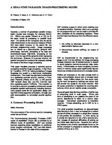
THE VLSI IMPLEMENTATION This chip is organized in two parts: the network module which interconnects one memory bank to 5 PEs, and the PE module which is interconnected to 5 memory banks through 5 network modules. Figure 1 depicts this structure.
2
memory bank link
left PEs
Network module Network
right PEs
conflicts unit
Processor module ALU1 Registers file
Instructions memory
ALU2
UC
Others memory banks (processor output)
Figure 1: internal diagram of a processor with 2 ALUs The processor structure is based on a VLIW organization [7] composed of a set of general registers and of a set of basic operators connected to each other. These basic operators are 16 bit integer ALUs. Such a size for the operands is currently used in Image Processing. As the ALUs are general purpose ones, they can perform address calculations as well as data calculations. The structure defined is such that at each instruction of one clock cycle, each PE can perform 2 arithmetic or logical operations and the access to the next instruction. In addition, an external memory access is performed in 2 clock cycles in parallel with the internal operations. The control unit is a RISC I-like structure. There is a single instruction format. This instruction format is presented in figure 2. The different fields are dedicated to the external memory access, the synchronization of the PEs, the conditionnal branches, the constant input and the two operations on the two ALUs. Dout1 is the register number of the result of the operation F1 on the first ALU. The instruction size is 54 bits.
MEM SYNC BCC CTE Din1 Din2 F1 Dout1 Din3 Din4 F2 Dout2
figure 2: instruction fields
3
The last part is the program memory which is loaded before the execution of the program by the use of one of the external links with the other chips. The states of the PE are then the execution mode, the sleeping mode and the program loading mode. The next module is the interconnection network. This network is such that each processor can have direct access to a subset of consecutive memory banks without routing conflicts with other processors. This concept of overlapped shared memories has been used in the OSMMA project [8]. To get round the limitations of this network, access to a distant memory bank which is not directly accessible needs several steps using intermediate processors. We have defined a path from each memory link to the associated processor output. Thus in synchronous mode, a data and its address arrived at the output toward a memory bank, can be leaded through the processor output toward an other memory bank. This type of operating mode is like a shift register mechanism. Each transfer can be performed at each clock cycle. The intermediate PE must participate by software in the distant access. Figure 3 shows the direct access capabilities of each processor in the general case. The network we have integrated in the VLSI chip has p=5 memory banks accessible per processor. The management conflict system associated to the network is used in MIMD mode to manage the simultaneous accesses of different PEs to a same memory bank. This system uses a rotating priorities mechanism to select a PE among several conflicting PEs.
p j
memories
j+1
j+p-1
j+p
network i
i+1
processors figure 3: general diagram of the network. The component has been designed with 1.2 CMOS standard cell. It is composed of 6 main parts designed separately: The network, the memory conflict management system, the 2 ALUs, the multiported register file with a local memory (128*16 bit RAM), the control unit and the program load system with the program memory (a 256*54 bit instruction RAM). The total area of the 140 pins chip is 90 mm2 with a heart area of 64 mm2. Figure 4 is the chip die of this component and figure 5 reports the different parts of the heart of the component. This chip has been designed with the CADENCE SOLO2030 [9] tools using the ES2 standard cell library. We can see on the chip die the main macro-cells of the 3 RAMs and the 2 multipliers, and all the other standard cells automatically placed and routed by the tools.
4
figure 4: chip die area % 1%
multiplier
18.5 % ALU (other parts) conflicts management
8.3 % 2%
interconnexion network
8%
10 %
registers local memory programme memory constante memory
47 % 2.3 %
47 %
11.4 % 3%
16.7 %
programme load system
6%
control unit
1.6 %
7.6 %
figure 5: area of each part
5
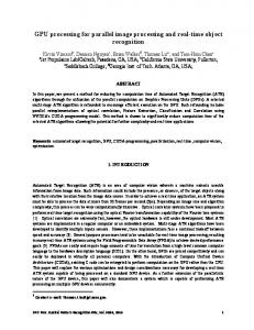
To build the whole architecture, several chips are organized in a linear manner as reported in figure 6. In this figure, only the links between one processor and its neighboors are represented. The other processor links are similar. The memory banks are linked on the top of the chips (one per chip). An example of distant access is presented in dotted lines, from the PE on the left to the memory bank on the right, via one intermediaite chip.
Figure 6: links between 1 chip and its neighboors
PERFORMANCE ANALYSIS We have studied a set of typical Image Processing algorithms making use at high rate of local or global memory accesses in synchronous mode. Figure 7 shows the general results obtained with these algorithms with 256*256 images and a structure with 16 processors each having 2 ALUs. level
pixel
global
algorithms
memory access
Thresholded
0.8 ms
100 %
logical operation
1.2 ms
100 %
histogram
1.1 ms
92.5 %
image reduction
1 ms
100 %
transposition
1 ms
84 %
skeleton
2 ms
100 %
3*3 convolution
4 ms
100 %
5.3 ms
75 % 87.5 %
DRF edge detection local
execution time
3*3 Prewitt
3.2 ms
split 3*3 dilation
2.4 ms
100 %
boarder distances
3.6 ms
80 %
figure 7: general results
6
With these examples, the network is used at more than 75%. These examples are then I/O-bounded, that is the external memory accesses define the execution time of the algorithms. In this case, it is the external memories that are restrictive. With some other algorithms having a more important treatment rate according to the memory accesses, it is the operative part of the processors that is restrictive. For these low level algorithms it is the synchronous mode that is usually used. The algorithms using global communications like the transposition or the reduction are not scalable when the number of processors is increased. We have studied for this algorithm the increase of the processor number and the increase of the access capability of each processor. The results obtained with 256*256 images are presented in figure 8. acc. cap. nb. PEs
8
16
32 _
16
1,1 ms
0,76 ms
32
1 ms
0,61 ms
0,39 ms
0,9 ms
0,5 ms
0,3 ms
0,87 ms
0,46 ms
0,25 ms
64 128
figure 8: results of the transposition algorithm for several configurations It can be noticed that for a constant value of the access capability p, the increase of the number of processors do not decrease in proportion the execution time of this algorithm, due to the increase of the amount of communications. In addition, the increase of the access capability p do not decrease the execution time in proportion although the cost of the network and its pins number is increased in proportion. Thus it is very interesting to limit the size of the access capability p. A typical global communication is the Broadcast of N values from N processors which is performed in N clock cycles. An example of treatment that takes advantage of this mechanism is the Hough transform in 2N directions. Each processor treating one direction has to receive all the edges of all the other processors. It is also possible to perform the internal operations of the Hough transform concurrently with the broadcasts, due to the orthogonal structure of the GFLOPS architecture. The advantages of MIMD operating mode are obvious for high level algorithms, where the data to be processed, which represent some image features extracted by the low level algorithms, have an irregular nature, and are thus badly suited to be processed in SIMD mode. Nevertheless, evaluation of this operating mode can only be obtained via a statistical process as the results reached are largely dependent on the data being processed and on the treatments. In addition, the methods used being on the whole different for each mode it will be difficult to compare the results. As an example of intermediate level algorithm, we have evaluated the connected component labelling problem in MIMD mode [10]. The region labelling is a basic operation in image processing. A labelled region represents a set of connected pixels. The purpose is to identify separately the different regions of the image. It consists of assigning the same number to all the
7
pixels belonging to the same region. The aim of the MIMD method is to reduce the amount of data to be propagated. This can be done if we work not at the pixel level but at the region level. Thus the image to be labelled is first cut into vertical segments which represents the nodes of a graph. This graph is distributed among the different memory banks in the same way as the image. Each node contains the following informations: - the edges with the right neighbouring segments, - the beginning and ending addresses of the segment, - the label initialized with zero. The aim of this algorithm is to give a unique label to the most left segments of the image and to propagate them from the left to the right along the edges of the graph. After each propagation, the processors are synchronized to test and stop the propagations. Then at the end of these propagations, a region is characterized by one or more labels. These different labels must be equal, and are broadcasted among the different processors which can get by a sorting algorithm the good value for each of its nodes. We can compare this algorithm with a synchronous algorithm using pixel propagations. Figure 9 describes these results with several 64*64 images and a 16-PE structure. chromosomes spiral chekerboard Abingdon cross
triton cells average
GFLOPS MIMD
0.08ms
0.2ms
0.05ms
0.1ms
0.06ms
0.08ms
GFLOPS SIMD
1.2ms
4ms
1ms
1ms
1.2ms
1.1ms
figure 9: results of the labelling algorithm in SIMD and MIMD modes. The average ratio between the SIMD and the MIMD algorithms performed on this architecture with different images is about 10. These performances are due to the fact that only the interesting information is propagated and not all the pixels of the image as with the SIMD algorithm. It shows that it is interesting to have a MIMD mode for intermediate and high level algorithms.
CONCLUSION In order to give an alternative to specialized processors in Image Processing, we have designed a multi-processor distributed memory architecture, in which the processors are linked to the various memory banks by a linearly expandable interconnecting network. The processors are autonomous but they can be synchronized by software. They are made up of standard ALUs. This allows an optimization of the amount of processing compared to the amount of memory accesses required for image processing. A functional simulation was made of the whole architecture (processors-network) for both synchronous and MIMD modes. In order to simulate an entire image processing chain, an evaluation of this architecture on high level algorithms has been undertaken. The implementation of the PEs has been presented. The physical implementation of the whole architecture has been started with a prototype composed of 32 processors. A second version of this component has been designed and will be integrated in
8
1993. This 240-pins chip will contain two 24-bit PEs with 3 ALUs each and a 1024-word instructions memory. These PEs will be able to deal with colour Image Processing at the video rate. The industrialization of GFLOPS will be studied according to this second version.
ACKNOWLEDGEMENTS The author would like to thank the CNRS GDR-ANM "Architectures Nouvelles de Machines" for its grant that supports this work.
References [1] D. Houzet, J.L. Basille, J.Y. Latil, "GFLOPS: A General Flexible Linearly Organized Parallel Structure for Images," IEEE ASAP'91, Barcelona, Sept. 1991, pp. 431-444. [2] D. Juvin, J.L. Basille, H. Essafi, J.Y. Latil, "Sympati2, a 1.5D Processor array for image applications," in EUSIPCO Signal processing IV: Theories and applications, North-Holland, 1988, pp. 311-314. [3] L.A. Schmitt, S.S. Wilson, "The AIS-5000 Parallele Processor," in Pattern Analysis and Machine Intelligence, 1987. [4] J.L. Basille, "How many dimensions for an array?," in Parallelism in Image Processing, Esprit BRA3035 Workshop, Bonas France, sept. 1990. [5] C.C. Weems, S.P. Levitan, A.R. Hanson, E.M. Riseman, D.B. Shu, J.G. Nash, "The Image Understanding Architecture," International Journal of Computer Vision, Kluwer Academic Publishers, Boston, 1989, pp. 251-282. [6] J.T. Kuehn, H.J. Siegel, D.L. Tuomenoksa, "The use and design of PASM," in Integrated Technology for Parallel Image Processing, ed. S. Levialdi, Academic Press, London, 1985, pp. 133-152. [7] J. A. Fisher, "Very Long Instruction Word Architectures and the ELI-512," 10th Symposium on Computer Architecture, IEEE Computer Society, 1983. [8] A.A. Naqvi & M.B. Sandler, "Performance of the OSMMA image processing system," in P.M. Dew, R.A. Earnshaw and T.R. Heywood eds., Parallel Processing for Computer Vision and Display, Addison-Wesley, NewYork, 1989, pp. 1532-1535. [9] European Silicon Structures (ES2), "SOLO 2030 reference manual", 1990. [10] P. Fernandez, D. Houzet, J.L. Basille, "Region Labelling in Image Processing with SIMD and MIMD architectures," CAMP'91, Paris, Dec. 1991, pp. 541-552.
9