compact predictive CMP model with dummy fill, and val- idate it with ... a lower wire density region, dummy fill is performed before ..... Pentinum-4 Linux machine.
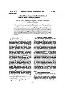
Wire Density Driven Global Routing for CMP Variation and Timing Minsik Cho, David Z. Pan
Hua Xiang, Ruchir Puri
ECE Dept. Univ. of Texas at Austin Austin, TX 78712 {mcho,dpan}@ece.utexas.edu
IBM T. J. Watson Research Center Yorktown Heights, NY 10598 {huaxiang,ruchir}@us.ibm.com
ABSTRACT In this paper, we propose the first wire density driven global routing that considers CMP variation and timing. To enable CMP awareness during global routing, we propose a compact predictive CMP model with dummy fill, and validate it with extensive industry data. While wire density has some correlation and similarity to the conventional congestion metric, they are indeed different in the global routing context. Therefore, wire density rather than congestion should be a unified metric to improve both CMP variation and timing. The proposed wire density driven global routing is implemented in a congestion-driven global router [5] for CMP and timing optimization. The new global router utilizes several novel techniques to reduce the wire density of CMP and timing hotspots. Our experimental results are very encouraging. The proposed algorithm improves CMP variation and timing by over 7% with negligible overhead in wirelength and even slightly better routability, compared to the pure congestion-driven global router [5].
Categories and Subject Descriptors B.7.2 [Hardware, Integrated Circuit]: Design Aids
General Terms Algorithms, Design, Performance
Keywords VLSI, Global Routing, Performance, Manufacturability
1. INTRODUCTION Aggressive technology scaling has led to much higher resistance and larger coupling capacitance on interconnect. According to ITRS roadmap [16], copper dishing/erosion after Chemical-Mechanical Polishing (CMP) and scattering effect may increase resistance significantly [7, 15, 29]. Also, coupling capacitance between wires becomes dominant over ground and fringing capacitance at 0.18µm technology (over 60% of the total capacitance), and increases This work is supported in part by SRC, IBM Faculty Award, Fujitsu, and equipment donations from Intel.
Permission to make digital or hard copies of all or part of this work for personal or classroom use is granted without fee provided that copies are not made or distributed for profit or commercial advantage and that copies bear this notice and the full citation on the first page. To copy otherwise, to republish, to post on servers or to redistribute to lists, requires prior specific permission and/or a fee. ICCAD 2006, November 5-9, 2006, San Jose, CA, USA. Copyright 2006 ACM 1-59593-389-1/06/0011 ...$5.00.
rapidly with higher wire aspect ratio of the advanced technologies [2, 26, 27]. Therefore, interconnect delay will suffer from the increased resistance and coupling capacitance more seriously in the future. Meanwhile, manufacturability and yield are becoming everserious concerns at 90nm node and below, and shown to be heavily affected by design patterns [21]. Especially, topography (thickness) variation after CMP is shown to be systematically determined by wire density distribution [19, 21, 29]. Even after CMP, intra-chip topography variation can still be on the order of 20-40% [9, 21]. Such topography variation leads to not only significant performance degradation due to increased wire resistance and capacitances, but also acute manufacturing issues like etching and printability [7, 9, 21, 23]. The main reason for the above problems is wire density distribution. Higher wire density usually leads to copper thickness reduction due to erosion after CMP [19, 29], making resistance worse. Also, the reduced copper thickness after CMP can worsen the scattering effect, further increasing resistance [15]. Meanwhile, a region with higher wire density tends to have less spacing between wires, thus significantly increasing coupling capacitance between them. For a lower wire density region, dummy fill is performed before CMP to make density distribution more uniform, expecting less topography variation after CMP. However, dummy fill is usually applied in the post-design stage, and has limitations due to strict rules (such as fill size, patten, spacing to other features) which intend to minimize the disturbance on the existing design. Thus, non-uniform distribution of density still exists even after the dummy fill, creating topography variation which wastes the minuscule depth of focus [6]. The global routing, as its name implies, is the routing stage that plans the approximate routing path of each net to reduce the complexity of routing task and guide the detailed router [14]. Thus, it has significant impact on wirelength, congestion/routability and wire density distribution, hence CMP variation and timing [7, 13, 14, 25]. The global routing should be an ideal stage for the first order to improve CMP variation as well as timing by optimizing wire density distribution [4, 26]. Even though there have been significant amount of work in global routing about crosstalk [4,10,17,18, 22,24,30], timing [4,13,26,28] and congestion/routability [1, 5, 8], none of them has worked on the optimization of wire density distribution for CMP variation and timing. In this paper, we propose a new paradigm of wire density driven global routing to improve CMP variation and timing. To our best knowledge, this is the first work that takes
Table 1: The notations in this paper.
wire density distribution into account to enhance both CMP variation and timing, while considering congestion and wirelength. Essentially, the proposed algorithm minimizes the wire density around timing critical nets to enhance timing, and the wire density of dense global routing cells to reduce topography variation after CMP. The major contributions of this paper include the following.
vi wi di mi ti li ni pi si tsi eij rij cij gij
• We present a simple predictive CMP model verified with industrial cases for the first time. We also show that only few regions of a chip are responsible for most of topography variation after CMP. This means that selective optimization of wire density distribution can enhance the uniformity of topography. • We use the wire density to guide global routing for CMP variation and timing. We show that wire density and congestion are not linearly proportional to each other. This implies that just congestion-driven global routing cannot address the wire density issue efficiently. Furthermore, we observe that wire delay is near linearly proportional to wire density in global routing even with CMP effect (dishing/erosion and dummy fill) [9, 20, 29] and scattering effect [15] taken into consideration.
Our approach achieves better timing and less topography variation than the state-of-the-art academic congestiondriven router [5] with negligible overhead on wirelength, and even better congestion/routability. The rest of the paper is organized as follows. In Section 2, preliminaries are described. A predictive CMP model is presented, and timing impact with wire density distribution is analyzed in Section 3. In Section 4, a wire density driven global routing is proposed. Experimental results are discussed in Section 5. Section 6 concludes this paper.
2. PRELIMINARIES 2.1 Global Routing Model The global routing problem can be modelled as a grid graph G(V, E), where each vertex vi represents a rectangular region of the chip, so called a global routing cell (G-cell), and each edge eij represents the boundary between vi and vj with a given maximum routing resource rij . A global routing is to find paths that connect the pins inside the Gcells through G(V, E) for each net.
2.2 Global Routing Metrics The key task of global router is to maximize (minimize) the routability (congestion) for successful detailed routing [25]. In addition, timing, manufacturability, and wirelength are other important goals of global router. • Routability can be estimated by the number of overflow s which indicates that routing demand locally exceeds the available routing capacity [25] [17]. Formal definition of overflow is in [17].
• Timing is a significant design objective, as interconnect which governs the overall system performance is mainly determined by global routing [13, 26]. • Manufacturability is no longer an optional objective in deep submicron region. In global routing, CMP variation which is a macro systematic variation due to wire density distribution can be optimized, as global router plans approximate routing path for each net [14]. • Wirelength is an important metric for placement as well as routing. But, it is less concern for global routing, as routing all wires with shortest path algorithms will result in minimum or near-minimum wirelength [25].
3.
PREDICTIVE CMP MODEL AND TIMING IMPACT WITH WIRE DENSITY
In this section, we propose a predictive CMP model for the first time. It is followed by the study of the timing impact of wire density under CMP (topography variation and dummy fill) [7] and scattering effect [15]. Then, we show that congestion driven routing cannot replace wire density driven routing, even though they are closely related.
3.1
Wire Density and Predictive CMP Model
Topography variation (thickness variation) after CMP is determined by underlying metal density which includes both wires and dummies. As dummy fill in turn depends on wire density, the required dummy density and the copper(Cu) thickness can be predicted from a given wire density. In Fig. 1, normalized Cu thickness change by metal density is shown based on three industrial designs. For a given G-cell vi with a metal density mi , we discover the Cu thickness of vi , ti can be expressed as follows: ti = α(1 − Normalized copper thickness (ti)
• We propose several novel wire density driven routing techniques for CMP variation and timing optimizations, including minimum pin density routing, timing sensitivity map and CMP aware wire density distribution. Each technique helps global router to reduce the wire density around timing critical nets, while minimizing topography variation after CMP.
vertex / global routing cell i wire density of vi dummy density of vi metal density of vi copper thickness of vi width / height of vi number of signal wires in vi number of wide wires in vi average spacing between wires in vi timing sensitivity of vi edge between vi and vj maximum routing resource of eij available routing resource of eij congestion of eij
m2i ) β
(0.2 ≤ mi ≤ 0.8)
(1)
1 Design1 Design2 Design3 0.95
0.9
0.85 0.2
0.3
0.4
0.5
0.6
0.7
0.8
0.9
Metal density (mi)
Figure 1: Normalized Cu thickness by metal density
1
0.8
0.95
0.6
0.9
0.4
0.85
Normalized copper thickness (ti) Metal (Wire+Dummy) density (m ) i Dummy density (d )
0.2
0.8
i
0 0.1
0.2
0.3
0.4
0.5
0.6
Wire density (w )
0.7
0.8
0.75 0.9
based on Eq. (2):
Normalized copper thickness (ti)
Dummy / Metal density (di/mi)
1
R(wi ) =
C(wi ) = ǫ · f (wi )(
where α and β are technology dependent constants. Eq. (1) requires the metal density mi as an input which is essentially the summation of the wire density wi and the dummy density di in a global routing cell vi . Fig. 2 shows the required dummy density and the predicted Cu thickness with respect to wire density. For a given vi , di can be looked up with wi using Fig. 2, and then mi can be obtained by adding wi and di . Finally, the calculated mi can be fed into Eq. (1) to predict the Cu thickness ti . This predictive model is verified with a commercial CMP simulator [12] and industry test cases.
3.2 Wire Density and Timing For two adjacent wires, each has two capacitance components, coupling capacitance Cc between itself and the other wire, and ground capacitance Cg between itself and ground. Bakoglu [3] shows that wire delay on a distributed RC network contains the following delay component, D: ρ·l ǫ·l·w ǫ·l·t )( + ) (2) w·t h s
where Rd is the driver resistance, ρ is the resistivity of the wire, ǫ is the insulator dielectric constant, w, t and h are the wire width, thickness and distance from the substrate, respectively. And, l and s are the length and spacing between two coupled wires, respectively. In Eq. (2), h is a constant and w can be assumed to be a constant as well (we do not consider the width variation effect in this paper as it is relatively small for Cu process). Without loss of generality, we just use the nominal wire width. For a given G-cell vi , ti is essentially a function of wi (mi depends on wi as in Fig. 2), and can be denoted as ti (wi ). If even spacing between wires and square G-cell are assumed, spacing between wires si becomes a function of wi : 1 − wi 1 ∝ −1 ni + pi wi
(0 < wi ≤ 1)
(3)
Also, we can obtain the increased total capacitance due to dummy fill (dummy increases coupling capacitance) as a function of wi based on [20]: f (wi ) = 1 + γ log(
si (wi ) ) δ
li · ti (wi ) li · Wnom + ) h si (wi )
(6) (7)
We observe the following with 65nm technology node: • Lower wire density shows less resistance (less erosion after CMP) as well as less capacitance (more spacing between wires). • Resistance variation dependence on wire density (computed post dummy fill and CMP estimation) is relatively smaller than capacitance variation. • D(wi ) is near linearly proportional to wi in the region where most of wire densities exist (see Eq. (3) and (6)).
Figure 2: Predictive CMP model
si (wi ) = li ·
(5)
D(wi ) ∝ (Rd + R(wi ))C(wi ) ∝ wi
i
D ∝ (Rd +r·l)(Cg +Cc ) = (Rd +
ρ(wi ) · li ti (wi ) · Wnom
3.3
Wire Density and Congestion
While congestion/routability has been the main concern in global routing, wire density distribution is an emerging important objective due to CMP variation and timing as shown in Section 3.1 and 3.2. Although wire density is closely related to congestion, congestion driven global routing cannot address wire density issues directly and effectively, because wire density is computed for the wires inside a global routing cell, while congestion is computed for the wires crossing the edges of a global routing cell. Fig. 3 shows a G-cell with edge A and B. When there is a wide wire such as power/ground as in Fig. 3 (a), density is not a half of congestion. Even though Fig. 3 (a) and (b) have the same density, Fig. 3 (b) is less congested. As wire density and congestion can be significantly different, wire density cannot be replaced with congestion; as a unified metric, wire density should be directly addressed in global routing for the optimization of CMP variation and timing.
4.
WIRE DENSITY DRIVEN GLOBAL ROUTING FOR CMP AND TIMING
In this section, we propose our wire density driven global routing algorithm which essentially minimizes the delay of timing critical nets by decreasing the wire density around such nets, and improves the topography variation after CMP by decreasing the wire density of dense G-cells selectively. Our approach consists of four ideas which can be easily integrated with any existing global router [1, 5, 8, 17]; minimum pin density routing in Section 4.1, timing sensitivity map in Section 4.2, selective wire density optimization for CMP awareness in Section 4.3, and wire density driven maze routing in Section 4.4.
A
A
B
B
(a) den=50%, gA =gB =100%
(b) den=50%, gA =gB =71%
(4)
where γ and δ are technology dependent constants. Note that f (wi ) is typically less than 1.1, and saturates quickly. Due to scattering effect under a given temperature, ρ is a function of ti . Thus, it is also a function of wi (see Eq. (1)), and can be denoted as ρ(wi ) [15]. Finally, the component of the wire delay in vi can be rewritten as a function of wi
Figure 3: Difference between congestion and density
S
a
a
S
C(we)
E
S2
Non-critical Sink
0.75
D C(wd)
b
D
D
b
(a) two possible paths forD-S (b) path b with higher density
D1 Driver
B
A
C
4.2 Timing Sensitivity Map Construction As Elmore delay can be expressed as the summation of RC product where C is the downstream capacitance seen by R in the distributed RC network, a capacitance close to the sink has more impact on timing than one close to the driver. Also, the capacitance of a G-cell where more timing critical nets are passing has more impact on timing. Thus, we can compute the sensitivity of each G-cell to timing, and construct the timing sensitivity map. As resistance is relatively insensitive to wire density variation (see Section 3.2), we consider only capacitance in constructing the timing sensitivity map. Fig. 5 illustrates how to construct timing sensitivity map. Given a net D1 -S1 -S2 as in Fig. 5 (a), if nominal resistance R is assumed for each G-cell (see Section 3.2), a part of Elmore delay from D1 to S1 can be written as follows: Delay
∝
RC(wa ) + 2RC(wb ) + 4RC(wf )
+
3{RC(wc ) + RC(wd ) + RC(we )}
As mentioned in Section 3.2, RC wire delay in a G-cell vi is near linearly proportional to wi . Thus, the above delay equation can be further simplified as follows: Delay
∝
wa + 2wb + 4wf + 3{wc + wd + we }
It is clear that each wire segment (thus, each G-cell) has different impact on the timing due to its geometrical location (whether it is close to driver or not). For example, 10% increase of wf has the same impact as 40% increase of wa
0.75 F
C(wa) C(wb) C(wc) C(wf)
D2
In practice, timing critical nets are commonly routed before other nets for the minimum length. As there can be multiple paths with the minimum length, a router can choose any of those based on its policy. However, we find that a path with the minimum pin density is better for the wire density distribution. In Fig. 4, a net D-S to be routed is shown with a pin distribution. If only L-shape routing is allowed, we can have two possible paths, a and b with the same length but different pin densities. As the existence of a pin means a connection to other pins, a path with higher pin density like b tends to have higher wire density eventually as in Fig. 4 (b), resulting in higher resistance and larger coupling capacitance. More importantly, the path with higher pin density cannot get much benefit from the wire density optimization, as there is little room for improvement (it is destined to have high wire density from the beginning). Note only L/Z-shape routing is considered in the minimum pin density routing to minimize the number of vias in our implementation.
Non-critical Sink
D1 S1 Critical Driver Sink
S1
0.25
0.5
0.75
1
Critical Sink
(a) Elmore delay of D1 -S1 -S2 (b) G-cell weights from D1 -S1 -S2
Figure 4: Example of minimum pin density routing
4.1 Minimum Pin Density Routing
S2
0.25
0.5
0.25
0.5
D1 Driver
0.75 D 1.5 C 1.75 S3
S2
Non-critical Sink
D3
0
0
0.25
0.5
S1
1
Critical Sink
(c) updated weight after D2 -S3
0.25
0.5
0.75 D 1.5 C 1.75
0 0 S4 1
(d) routed non-critical D3 -S4
Figure 5: Example of timing sensitivity map construction on timing. Therefore, each G-cell can have its own time sensitivity to the density change as in Fig. 5 (b). We can apply the same idea to all the timing critical nets which are already routed by the minimum pin density routing, and sum up the timing sensitivity from each net to construct a timing sensitivity map. For example, in Fig. 5 (c), another timing critical net D2 -S3 is joining the net D1 -S1 -S2 at the G-cell vC and vD . As vC has already 0.75 as the timing sensitivity tsC , after considering D2 -S3 , tsC becomes 1.75 due to 1 from D2 -S3 . In the same manner, tsD becomes 1.5 due to another 0.75 from D2 -S3 . With the timing sensitivity of each G-cell, we can make a non-timing critical net D3 -S4 detour to reduce the wire density of the highly timing sensitive G-cell like vD as in Fig. 5 (d). This improves the overall timing by reducing the wire density of more timing sensitive G-cells, while minimizing the overhead in wirelength. Algorithm 1 shows how to construct the timing sensitivity map.
4.3
CMP Aware Wire Density Distribution
To improve CMP variation, more uniform metal density distribution should be achieved by increasing density for less dense G-cells or decreasing density for more dense G-cells. Algorithm 1 Timing Sensitivity Map Construction Input: List of timing critical nets and G-cells 1: tsi = 0 ∀ G-cell i 2: for each timing critical net N do 3: P = Path from critical sink S to driver D 4: Ls = Path length from S to D 5: for each G-cell vj ∈ P do 6: Lj = Path length from vj to D 7: tsj = tsj +Lj /Ls 8: end for 9: for each G-cell vj ∈ / P, ∈ N do 10: vx = G-cell closest to vx ∈ P 11: Lx = Path length from vx to D 12: tsj = tsj +Lx /Ls 13: end for 14: end for Output: Timing sensitivity map
0.12 0.1 0.08 0.06 0.04 0.02 0 0.82
0.84
0.86
0.88
0.9
0.92
0.94
0.96
0.98
1
Normalized copper thickness
Figure 6: Normalized Cu thickness distributions of four industrial designs We find that reducing wire density of the more dense G-cells can be more effective than the other way for two reasons. First, it requires to perturb smaller number of G-cells. Fig. 6 shows Cu thickness distributions of four industrial cases after CMP. It shows only few G-cells have over 5% of Cu loss, and are mainly responsible for topography variation. Thus, optimizing G-cells over a threshold metal density Td can make topography more uniform without disturbing other design objectives. Second, lowering wire density also helps congestion as they are correlated.
4.4 Wire Density Driven Maze Routing The wire density distribution governs both CMP variation and timing. The objective for timing requires lower density for the timing sensitive G-cell, and the objective for CMP variation requires lower density for the G-cells above the threshold of Section 4.3. The wire density driven maze routing is shown in Algorithm 2. Note that mi can be computed from the CMP model in Section 3.1, and Costo are for other design objectives such as congestion. Two parameters, P and Q are introduced to control the trade-off between objectives.
5. EXPERIMENTAL RESULTS We implement the proposed algorithm in C++ by modifying BoxRouter [5], and compare the results with the original BoxRouter. All the experiments are performed on a 2.8 GHz Pentinum-4 Linux machine. The ISPD98 IBM benchmarks are taken from [11], and we modify the horizontal and vertical capacity of each circuit as shown in Table 2. Further, assuming up to 30% of routing capacity is assigned for wide wires like power/ground, we reduce the routing capacity to get enough number of overflows (to see the impact on congestion/routability), and make the horizontal and the vertical capacity same for easy wire density calculation. Since the original benchmarks do not have any timing informaAlgorithm 2 Wire Density Driven Maze Routing Input: G-cell vi and Parameter P, Q, Td 1: Cost C = Costo //from other optimization costs 2: if tsi > 0 then 3: C += P · wi · (1 + tsi ) //timing sensitivity 4: else if mi > Td then 5: C += Q · wi //CMP awareness 6: end if Output: C
6.
CONCLUSION
In nanometer design, wire density should be a key metric for manufacturability and timing optimization. We present the first wire density driven global routing to improve CMP variation and timing based on the predictive CMP model and several novel techniques. Experimental results are highly encouraging, showing that the proposed algorithm outperforms the state-of-the-art congestion driven global router in terms of CMP variation and timing with negligible overhead in wirelength, and even slightly better routability. 5 Wirelength Total Delay Max Delay
0 −5 −10 0
1
2
3
4
5
P
6
7
(a) P with Q=0
8
9
10
Delay, wirelength and topography var. change(%)
0.14
tion, we randomly pick less than 1% nets which are longer than 200µm as optimization targets. HSPICE simulation with 65nm technology is performed to estimate timing with CMP variation and scattering effect taken into account. All the timing critical nets are pre-routed in the same minimum length and same topology in any experiment to eliminate the effect of different path lengths and topologies on timing. Fig. 7 (a) shows total/max delay and wirelength change by the parameter P with Q=0. While the wirelength increases as P increases, the delay decreases until P =1, and then starts increasing after that. The reason is because too much increase in wirelength due to detouring around timing sensitive G-cells (with higher P value), finally makes overall congestion worse. This provokes the congestion driven objective to push wires back to the timing sensitive G-cells. All the following simulations use P =1, as it shows reasonable trade-off. Fig. 7 (b) shows total/max delay, wirelength and topography variation change by the parameter Q with P =1. While the total delay and max delay increase with larger Q, the topography variation decreases. Wirelength does not change noticeably, proving that our selective wire density optimization for CMP variation is friendly with other design objectives. Although the topography variation can be improved by over 10% with large Q, all the following simulations use Q=1.3 for the minimal impact on timing. Table 2 shows the experimental results and comparison of the proposed algorithm (the modified BoxRouter) with the original BoxRouter. The experiment sets P =1, Q=1.3 and Td =0.33 of Algorithm 2 to evaluate the optimization for CMP variation and timing together. The average of total delay and max delay are slightly reduced to 7.0% and 8.0% respectively, while topography variation after CMP is improved by 7.5% on average and up to 10.1%. The overhead in CPU time is still only 41% on average. Also routability is improved, as the number of G-cells with high wire density (which tend to be congested) is reduced by CMP aware wire density distribution. As already shown in Fig. 7 (b), wirelength overhead is quite small, and the improved routability even suppresses the increase in wirelength (less detouring).
Delay and wirelength change (%)
Normalized number of G−cells
0.16
0 Wirelength Total delay Max delay Topography variation
−2 −4 −6 −8 −10 0.5
1
Q
1.5
(b) Q with P =1
Figure 7: Effectiveness of parameter P and Q
2
Table 2: Comparison with BoxRouter for ISPD98 Benchmarks. circuit name hz. cap ibm01 18 ibm02 36 ibm03 31 ibm04 26 ibm05 45 ibm06 35 ibm07 34 ibm08 31 ibm09 25 ibm10 43
vt. cap 18 36 31 26 45 35 34 31 25 43
BoxRouter t.delam.delb wlenc ovflddume t.vf (ns) (ps) (%) 0.57 30.1 61374 4 372 1.34 1.85 67.6 180816 25 357 1.94 1.91 75.7 148530 5 389 1.73 1.61 61.4 167557 99 441 1.75 3.75 252.2 426547 100 542 1.78 2.10 243.8 283836 11 540 1.42 1.77 100.7 372268 18 867 1.67 2.62 191.8 420609 72 770 1.72 2.32 192.8 432120 75 1091 1.59 3.21 799.0 584100 33 1183 1.48
cpu (sec) 7.1 34.8 16.0 20.0 51.1 33.1 46.5 94.2 68.8 90.5
Wire Density Driven BoxRouter t.del m.del wlen ovfl dum t.v cpu (ns) (ps) (%) (sec) 0.53 26.3 61512 5 366 1.31 8.7 1.74 66.3 180399 26 358 1.90 44.7 1.77 69.4 150274 6 389 1.75 23.7 1.47 58.2 168307 100 437 1.75 26.4 3.41 219.3 432529 85 539 1.84 77.7 1.93 228.0 286783 8 541 1.46 49.7 1.62 93.1 374954 17 871 1.68 63.1 2.36 162.4 423634 62 770 1.74 121.7 2.13 170.4 435230 70 1088 1.58 88.1 2.85 711.4 589234 32 1166 1.48 122.3 average
Change (%) t.del m.del wlen ovfl dum t.v cpu -6.7 -6.0 -7.0 -8.4 -9.1 -8.3 -8.3 -10.0 -8.3 -11.4 -7.0
-12.5 -2.0 -8.4 -5.2 -13.0 -6.5 -7.5 -15.3 -11.6 -11.0 -8.0
0.2 -0.2 1.2 0.4 1.4 1.0 0.7 0.7 0.7 0.9 0.0
25.0 4.0 20.0 1.0 -15.0 -27.3 -5.6 -13.9 -6.7 -3.0 -28.6
-1.6 0.3 0.0 -0.9 -0.6 0.2 0.5 0.0 -0.3 -1.4 -2.2
-2.2 -2.1 1.2 0.0 3.4 2.8 0.6 1.2 -0.6 0.0 -7.5
22.5 28.4 48.1 32.0 52.1 50.2 35.7 29.2 28.1 35.1 40.9
(a) total delay (b) max delay (c) wirelength (d) overflow (e) the amount of dummy (f) topography variation after dummy fill(std/avg)
7. REFERENCES
[1] C. Albrecht. Global Routing by New Approximation Algorithms for Multicommodity Flow. IEEE Trans. on Computer-Aided Design of Integrated Circuits and Systems, 20, May 2001. [2] R. Arunachaiam, K. rajagopal, and L. T. Pileggi. TACO: Timing Analysis with COupling. In Proc. Design Automation Conf., June 2000. [3] H. B. Bakoglu. Circuits, Interconnections, and Packaging for VLSI. In Addison-Wesley Publishing Company, 1990. [4] M. R. Becer, D. Blaauw, R. Panda, and I. N. Hajj. Early Probabilistic Noise Estimation for Capacitively Coupled Interconnects. IEEE Trans. on Computer-Aided Design of Integrated Circuits and Systems, 22, March 2003. [5] M. Cho and D. Z. Pan. BoxRouter: A New Global Router Based on Box Expansion and Progressive ILP. In Proc. Design Automation Conf., July 2006. [6] S. J. Fang, T. H. Smith, G. B. Shinn, J. A. Stefani, and D. S. Boning. Advanced Process Control in Dielectric Chemical Mechanical Polishing (CMP). In Chemical Mechanical Polish for ULSI Multilevel Interconnection Conference, Feb 1999. [7] T. E. Gbondo-Tugbawa. Chip-Scale Modeling of Pattern Dependencies in Copper Chemical Mechanical Polishing Process. In Ph.D. Thesis, Massachusetts Institute of Technology, 2002. [8] R. T. Hadsell and P. H. Madden. Improved Global Routing through Congestion Estimation. In Proc. Design Automation Conf., June 2003. [9] L. He, A. B. Kahng, K. Tam, and J. Xiong. Design of IC Interconnects with Accurate Modeling of CMP. In Int. Society for Optical Engineering (SPIE) Symp. on Microlithograhpy, Mar 2005. [10] T.-Y. Ho, Y.-W. Change, S.-J. Chen, and D. T. Lee. A Fast Crosstalk- and Performance-Driven Multilevel Routing System. In Proc. Int. Conf. on Computer Aided Design, Nov 2003. [11] http://www.ece.ucsb.edu/∼kastner/labyrinth/. [12] http://www.praesagus.com/. [13] J. Hu and S. Sapatnekar. A Timing-Constrained Algorithm for Simultaneous Global Routing of Multimple Nets. In Proc. Int. Conf. on Computer Aided Design, 2000. [14] J. Hu and S. Sapatnekar. A Survey On Multi-net Global Routing for Integrated Circuits. Integration, the VLSI Journal, 31, 2002. [15] S. Im, N. Srivastava, K. Banerjee, and K. E. Goodson. Scaling Analysis of Multilevel Interconnect Temperatrues for High-Performance ICs. IEEE Trans. on Electron Devices, 52, Dec 2005. [16] International Technology Roadmap for Semiconductors (ITRS). 2005. [17] R. Kastner, E. Bozorgzadeh, and M. Sarrafzadeh. Pattern Routing: Use and Theory for Increasing Predictability and Avoiding Coupling. IEEE Trans. on Computer-Aided
Design of Integrated Circuits and Systems, 21, July 2002. [18] D. A. Kirkpatrick and A. L. Sangiovanni-Vincentelli. Techniques For Crosstalk Avoidance In The Physical Design Of High-performance Digital Systems. In Proc. Int. Conf. on Computer Aided Design, 1994. [19] S. Lakshminarayanan, P. J. Wright, and J. Pallinti. Electrical characterization of the copper CMP process and derivation of metal layout rules. IEEE Trans. on Semiconductor Manufacturing, 16, Nov 2003. [20] W.-S. Lee, K.-H. Lee, J.-K. Park, T.-K. Kim, and Y.-K. Park. Investigation of the capacitance deviation due to metal-fills and the effective interconnect geometry modeling. In Proc. Int. Symp. on Quality Electronic Design, Nov 2003. [21] X. Qi, A. Gyure, Y. Luo, S. C. Lo, M. Shahram, and K. Singhal. Emerging technologies: Measurement and characterization of pattern dependent process variations of interconnect resistance, capacitance and inductance in nanometer technologies. In ACM Great Lakes symposium on VLSI, April 2006. [22] P. Saxena and S. Gupta. On Integrating Power and Signal Routing for Shield Count Minimization in Congested Regions. IEEE Trans. on Computer-Aided Design of Integrated Circuits and Systems, 22, April 2003. [23] R. Tian, D. F. Wong, and R. Boone. Model-Based Dummy Feature Placement for Oxide Chemical-Mechanical Polishing Manufacturability. IEEE Trans. on Computer-Aided Design of Integrated Circuits and Systems, 20, 2001. [24] A. Vittal and M. Marek-Sadowska. Crosstalk reduction for VLSI. IEEE Trans. on Computer-Aided Design of Integrated Circuits and Systems, 16, March 1997. [25] J. Westra, P. Groeneveld, T. Yan, and P. H. Madden. Global Routing: Metrics, Benchmarks, and Tools. In IEEE DATC Electronic Design Process, April 2005. [26] D. Wu, J. Hu, and R. Mahapatra. Coupling Aware Timing Optimization and Antenna Avoidance in Layer Assignment. In Proc. Int. Symp. on Physical Design, April 2005. [27] D. Wu, J. Hu, M. Zhao, and R. Mahapatra. Timing Driven Track Routing Considering Coupling Capacitance. In Proc. Asia and South Pacific Design Automation Conf., 2005. [28] J. Xu, X. Hong, T. Jing, Y. Cai, and J. Gu. A Novel Timing-Driven Global Routing Algorithm Considering Coupling Effects for High Performance Circuit Design. In Proc. Asia and South Pacific Design Automation Conf., Jan 2003. [29] P. Zarkesh-Ha, S. Lakshminarayann, K. Doniger, W. Loh, and P. Wright. Impact of Interconnect Pattern Density Information on a 90nm Technology ASIC Design Flow. In Proc. Int. Symp. on Quality Electronic Design, Nov 2003. [30] H. Zhou and D. F. Wong. Global routing with crosstalk constraints. IEEE Trans. on Computer-Aided Design of Integrated Circuits and Systems, 18, Nov 1998.