Microscopic understanding and modeling of HfO2 RRAM device physics. L. Larcher, A. Padovani, O. Pirrotta, L. Vandelli, G. Bersuker1. DISMI, Università di ...
Microscopic understanding and modeling of HfO2 RRAM device physics L. Larcher, A. Padovani, O. Pirrotta, L. Vandelli, G. Bersuker1 DISMI, Università di Modena e Reggio Emilia, 42122 Reggio Emilia, Italy 1 SEMATECH, 2706 Montopolis Dr., Austin, TX 78741, USA dielectric physical thicknesses, the leakage current across HfOx is by several orders of magnitudes higher than that in HfO2, whereas the temperature dependency and the extracted activation energies of the conduction processes in these stacks are very similar. TAT current simulations, which accurately reproduce the experimental leakage currents, indicate that GBs (that cover only few percent of the total device area (3) have a much larger density of O vacancies in the case of HfOx than that in HfO2, as expected due to oxygen gettering by the overlaying Ti metal film. The vacancy density is thus expected to be larger near the metal layer (6, 7). This underlines the importance of GBs, which are the preferential locations for the defect accumulation and generation, and can be therefore considered as the CF precursors. In the amorphous HfOx, molecular dynamic simulations show that the dielectric may phase separate into stoichiometric HfO2 regions and Hf-rich domains, supporting a charge transport process similar to that along the GBs.
Abstract In this paper we investigate the physical mechanisms governing operations in HfOx RRAM devices. Forming set and reset processes are studied using a model including power dissipation associated with the charge transport, and the corresponding temperature increase, which assists ion diffusion. Introduction Filament-based bipolar resistive memories (RRAM) employing hafnium oxide dielectrics are a promising nonvolatile memory technology. Optimizing the materials (e.g. the oxide stoichiometry) and the device structure (e.g. multiple stacks, metal interfaces) for ensuring reliable switching operations requires a deep understanding of the microscopic properties of the conductive filament created during the initial forming operation. The forming operation, which sets the initial conditions, is believed to be related to the formation of a dominant conductive filament, CF, which can be then partially disrupted and reformed during reset and set operations, respectively. Despite multiple attempts (1, 2), a consistent quantitative description of the physical mechanisms governing RRAM operations has not been presented yet. In this study, we propose a comprehensive model strictly based on the material atomistic properties for explaining the physical mechanisms governing RRAM device operations. We derive useful insights about the role of charge transport through the dielectric film and on the CF formation and the oxygen ion diffusion process, which are important to understand the factors responsible for reliable switching and endurance in RRAM devices.
The conductive filament: formation and features.
Current Density [A/cm2]
The quantitative description of the characteristics of the conductive filament is critical for understanding the physical mechanisms governing the RRAM device operations. This requires modeling the forming operation, which allows deriving the shape and resistance profile of the CF, as well as the distribution of O ions in the surrounding dielectric.
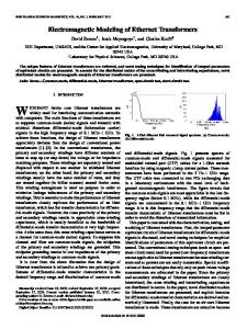
Leakage current and charge transport in HfOx The charge transport in poly-crystalline hafnium oxide has shown to occur preferentially at grain boundaries (GBs) (3), where the positively charge oxygen vacancies segregate. The dominant charge transport mechanism is the Trap-Assisted Tunneling (TAT) assisted by O vacancy defects, which is described by a quantum-mechanical model including electron-phonon coupling and lattice relaxation (4, 5). Figure 1 shows the leakage currents measured on MIM capacitors with stoichiometric HfO2 and substoichiometric HfOx hafnium oxide fabricated by depositing an overlaying Ti metal film. Despite the same
978-1-4673-4871-3/12/$31.00 ©2012 IEEE
symbols: experiments lines: simulations
1E+03 1E+01
sub-stoichiometric
1E-01 1E-03
30°C 60°C 90°C 120°C 150°C
1E-05 stoichiometric
1E-07 1E-09 0
0.5
1
1.5
Gate Voltage [V] Fig. 1. Leakage currents measured (symbols) and simulated (solid lines) at different temperatures on MIM capacitors with stoichiometric HfO2 and sub-stoichiometric HfOx hafnium oxide. Simulations are performed with the multiphonon TAT model proposed in (4, 5).
20.1.1
IEDM12-474
Cumulative prob. (F)
(a) capture emission
mjℏω0
njℏω0
(
)
Pj = R j ⋅ m j − n j ⋅ =ω0 [pW]
0.6 0.4 0.2 0.0
TiN
P(x, y, z ) = kTH ⋅ ∇ 2T (x, y, z ) [°K]
Forming Voltage [V]
Z [nm]
1.5
1.7
VFORMING[V]
3.0
750 600 450 300
Fig. 2. (a) Schematic representation of the energy-release process occurring at the trap sites during TAT for the simplified case of a single trap: Pj, Rj, mj and nj are respectively the power dissipated, the electron flow rate, the phonons emitted/absorbed at the j-th trap site; hω0 is the phonon energy. (b) 3D power dissipation map and (c) 3D temperature profile as derived from the simulation of a single GB containing 20 randomly distributed defects. kTH is the HfOx thermal conductivity.
1.9
⎛ E (x , y , z ) − b ⋅ F (x , y , z ) ⎞ ⎟⎟ G( x , y , z ) = ν ⋅ exp⎜⎜ − A k BT ( x , y , z ) ⎝ ⎠
tHfOx = 50Å Area = 5x5µm2
2.5
2.0
1.5
experiments simulations
10-6
10-4
10-2
100
Gate Current @ 0.5V [A] Fig. 4. Forming voltage versus leakage current measured on samples with an area of 5x5µm2 and a HfOx thickness of 5nm (11). Solid lines show simulations performed by the model in (7, 9).
The forming is modeled as a positive-feedback process (8, 9). The power dissipation associated with the TAT current is calculated within the multiphonon description from the energy released at every capture event by charge carriers to the portion of the lattice where the trap is located. The temperature (T) increase associated with this power dissipation is computed by solving the Fourier heat transfer equation, as shown in Fig. 2. The oxygen vacancy generation rate (G) depends exponentially on temperature and electric field (F) (8,10,12):
temperature, thus inducing a positive feedback loop. This process triggers the BD runaway leading to the formation of a CF. By modeling the forming process using the above description we successfully reproduced forming transients on single devices, as well as the statistical distribution of the forming voltages VFORM, as shown in Fig. 3 (9). The value considered for EA agrees with that calculated in (10) for the stoichiometric HfO2 (EA~4.5eV), whereas it is much lower for HfOx=1.85 (EA~3.0eV) (7), likely due to lower oxygen vacancy formation energy in more O deficient amorphous structures. Figure 4 shows that the leakage current, IG, is correlated to the forming voltage, independently from the dielectric and OEL thicknesses, and the device area (11). This IG-VFORM trend is related to the formation of a highly sub-stoichiometric thin HfOx layer close to the interface with the Ti electrode (7). This highly oxygen deficient layer supports a higher leakage current, promoting the formation of a preferential conductive filament controlled by the dielectric barrier corresponding to the oxide portion
(1)
kB is the Boltzmann’s constant; ν is the Debye vibration frequency; b is the bond polarization factor (8); EA is the effective defect formation energy at zero-field (8). Generation of new defects caused by field and temperature leads to a higher TAT current, which in turn results in more power dissipation and subsequently higher
IEDM12-475
1.3
Fig. 3. Cumulative VFORM distributions measured (symbols) and simulated (solid lines) across TiN/5nm HfO2/TiN at room temperature. Simulations have been performed using the model proposed in (8, 9).
TiN
(c)
simulations experiment
0.8
Z [nm]
(b)
1.0
20.1.2
with the lower O vacancy density. This explains the lower forming voltage observed in samples with the higher leakage current, as demonstrated by the forming simulations shown in Fig. 4 (11).
TE (TiN)
Z [nm]
(a)
Oxygen ion distributions after CF formation In order to understand the mechanisms responsible for the reliable switching in RRAM devices despite the stochastic nature of ion diffusion and the small number of O ions involved, we have extended the above forming model (8) by including the diffusion and recombination of oxygen ions and vacancies. Such processes are described through a kinetic Monte Carlo (kMC) model which allows reproducing the process statistic. The ion diffusion and recombination description is coupled with the model reproducing the charge-transport, the local temperature increase and the stress-induced generation of new oxygen vacancy/ion couples. Diffusion rates (RD) are calculated by
BE (TiN) Fig. 5. Oxygen vacancy (green dots) and ion (red dots) distributions simulated in the case of a RVF (voltage ramp rate = 1V/s). Device parameters and forming conditions are: 5nm-thick HfOx; T=25°C, 1µA current compliance.
that control the directional (i.e. vertical) and random (i.e. mainly radial) components of O ion diffusion, respectively. Besides moving along the CF, ions tend also to out-diffuse under the action of the internal temperature and Coulomb repulsion induced by other ions, Fig. 6(b). The interaction of O ions with the overlaying layer is still not unambiguously understood. If the O ions reach the top Ti metal, they could oxidize the Ti metal (this process is energetically favored), being completely lost and no more available for contributing to the subsequent reset operation. This would prevent to achieve a long endurance in RRAM devices. Storing the O ions in some favorable positions where they can be easily moved forward and back for achieving a reliable switching is essential for RRAM operations. We think that the thin TiOx layer formed at the HfOx interface during process (i.e. after the Ti after-deposition thermal annealing) prevents the O ion deep penetration into the top electrode because of the very high activation energy for O ion diffusion (17). Thus, O ions could be stored in some interstitial positions near the top interface, consistently with voids related by broken O-Hf bonds and the mechanical stress affecting the dielectric portion surrounding the CF. The O ion distribution is very important for understanding the mechanisms of subsequent reset operation, reliable switching, endurance (beyond 109 cycles) and retention.
⎛ E A ,D (x , y , z ) − λ Q ⋅ FEFF (x , y , z ) ⎞ ⎟ (2) 2 RD ( x , y , z ) = ν ⋅ exp⎜ − ⎜ ⎟ k BT ( x , y , z ) ⎝ ⎠ ,
where Q is the charge of the diffusing specie, λ = 3Å is the jump distance, and EA,D is the activation energy for ion/vacancy diffusion, given by EA,D=0.7eV and EA,D=1.5eV for O2- ions and positive O vacancies (13, 14), respectively. O vacancies are found to not move because of the large activation energy. FEFF is the effective field along the jump direction, calculated by taking into account the charge associated with O ions and vacancies. We modeled the recombination of O ions and vacancies by using an effective energy description with low activation energy of ∼0.2 eV (15). The ion diffusion and their distribution at the end of the forming operation depend on several factor, such as the current compliance (which determines the local temperature inside the CF), the forming mode (i.e. either ramped, RVF, or constant, CVF, voltage forming), and the voltage ramp rate, which can lead to current overshoot (16). Figure 5 show an example of the spatial O ion and vacancy distributions obtained from the simulations at the end of the RFV transient. Vacancies are distributed quite uniformly, indicating a regular CF resistance profile, whereas the O ions tend to accumulate near the top interface. The distributions of O ions along the vertical and radial coordinates are shown in Fig. 6(a)-(b) for both CVF and RVF, respectively. CVF leads to a slightly more uniform O ion distribution along the vertical CF direction, whereas O ions tend to accumulate more at the HfOx interface with the positively biased top Ti electrode during RVF. The O ion accumulation near the top interface is related to the different role played by field and temperature,
Ion diffusion for reliable switching Set and reset are believed to be related to the disruption and reconstruction of a dielectric barrier inside the CF, respectively (8, 18). The barrier disruption during set is successfully described as a field-induced dielectric breakdown process (8, 18).
20.1.3
IEDM12-476
120 100
Ions/nm
Conclusions
CVF
(a)
RVF
We investigated the main physical mechanisms involved in forming, set and reset operations of HfOx RRAM devices by using a physical description linked to the microscopic properties of the material. Simulation results underlined the importance of ion diffusion and the crucial role played by dielectric-metal interfaces, that are critical for both understanding and engineering RRAM device performance and reliability.
80 60 40 20 0 0
1
2
3
4
5
References
HfOx Thickness [nm] 120
CVF
(b)
100
Ions/nm
(1) S. Yu, R. Jeyasingh, Y. Wu, and H.-S. P. Wong, "Understanding the conduction and switching mechanism of metal oxide RRAM through low frequency noise and AC conductance measurement and analysis," IEEE International Electron Devices Meeting, December 2011, pp. 275-278. (2) D. Ielmini "Modeling the Universal Set/Reset Characteristics of Bipolar RRAM by Field- and Temperature-Driven Filament Growth," IEEE Trans. Electron Devices, vol. 58, pp. 4309-4317, December 2011. (3) V. Iglesias et al., "Correlation between the nanoscale electrical and morphological properties of crystallized hafnium oxide-based metal oxide semiconductor structures," Appl. Phys. Lett., vol. 97, p. 262906, 2010. (4) L. Larcher, "Simulation of leakage currents in MOS and Flash memory devices with a new multiphonon trap-assisted-tunneling model", IEEE Trans. Electron Devices, vol. 50, pp. 1246-1253, 2003. (5) L. Vandelli, A. Padovani, L. Larcher, R.G. Southwick III, W.B. Knowlton, and G. Bersuker, "A physical model of the temperature dependence of the current through SiO2/HfO2 stacks," IEEE Trans. Electron Devices, vol. 58, pp. 2878-2887, 2011. (6) D. Gilmer et al., "Asymmetry, vacancy engineering and mechanism for bipolar RRAM," IEEE International Memory Workshop, 2012, p. 49. (7) A. Padovani, L. Larcher, P. Pavan, C. Cagli and B. de Salvo, "Understanding the role of the Ti metal electrode on the forming of HfO2based RRAMs," IEEE International Memory Workshop, 2012, p.127. (8) L. Vandelli et al., "Comprehensive physical modeling of forming and switching operations in HfO2 RRAM devices," IEEE International Electron Devices Meeting, December, 2011, pp. 421-424. (9) L. Vandelli, A. Padovani, L. Larcher, G. Bersuker, D. Gilmer, and P. Pavan, "Modeling of the forming operation in HfO2-base resistive switching memories," 3rd IEEE International Memory Workshop, May 2011, pp. 119-122. (10) J. McPherson, J. Y. Kim, A. Shanware, H. Mogul, "Termochemical description of dielectric breakdown in high dielectric constant materials", Appl. Phys. Lett., vol. 82, pp. 2121-2123, 2003. (11) K. G. Young-Fisher, G. Bersuker, B. Butcher, A. Padovani, L. Larcher, D. C. Gilmer, "Correlation between Initial Leakage Current and Forming Voltage in HfOx RRAM Devices," unpublished. (12) G. Bersuker, Y. Jeon, and H. R. Huff, "Degradation of thin oxides during electrical stress," Microelectron. Reliab., vol. 41, p. 1923, 2003. (13) N. Capro, P. Broqvist and A. Pasquarello, "Migration of oxygen vacancy in HfO2 and across the HfO2 /SiO2 interface: a first-principles investigation, " Appl. Phys. Lett., vol. 91, p. 192905, 2007. (14) A. S. Foster, F. Lopez Gejo, A. L. Shluger, and R. M. Nieminen, "Vacancy and interstitial defects in hafnia," Phys. Rev. Lett., vol. 89, p. 225901, November 2002. (15) R. Govindaraj, C. S. Sundar, and R. Kesavamoorthy, “Atomic scale study of oxidation of hafnium: Formation of hafnium core and oxide shel,” J. Appl. Phys., vol. 100, 084318, 2006. (16) A. Kalantarian et al., "Controlling Uniformity of RRAM Characteristics via the Forming Process," IEEE International Reliability Physics Symposium, April 2012, pp. 6C.4.1-6C.4.5. (17) A. P. Brouma, N. M. Degnan, M. L. Meier, ”Oxygen diffusion into titanium,” ASEE Annual Conference Proceedings, p. 10783, 2003. (18) G. Bersuker et al. "Metal Oxide RRAM Switching Mechanism Based on Conductive Filament Properties," J. App. Phys., vol. 110, p. 124518, December 2011.
RVF
80 60 40 20 0 0
1
2
3
4
radial direction [nm] Fig. 6. Density of oxygen ions along (a) the CF and (b) the radial direction as obtained from the kMC simulations of ramped voltage forming (ramp rate = 1V/s) and constant voltage forming (VG = 1.2V) operations. Device parameters and forming conditions are: 5nm-thick HfOx; T=25°C, 1µA current compliance.
Conversely, the barrier reconstruction occurring during reset is a more complex physical process, requiring a relatively large temperature (induced by the power dissipation associated with the charge transport (8, 18) to support the diffusion of O ions and the recombination/oxidation process. In order to investigate the physics of this process, we performed reset simulations using the model described above by considering the initial distribution of O vacancies and ions extracted from forming simulations. As expected, the density of O vacancies along the CF is shown to reduce during the reset transient, leading to the formation of a potential barrier that is related to the resistance increase observed during the LRS to HRS transition (not shown for brevity). The dielectric barrier formed inside the CF during the reset operation depends on the resistance profile of the conductive filament, which affects in turn the power dissipation and temperature increase (8). Furthermore, simulations show that another important factor affecting the barrier formation is the proximity to the O ion reservoir and the role played by the metal electrodes. During subsequent set operation, O ions generated by the field-induced breakdown of the barrier inside the CF diffuse again toward the top interface driven by the field.
IEDM12-477
20.1.4