94GHz Single-Layer Slotted Waveguide Array by Diffusion Bonding of Laminated Thin Plates #
Jiro Hirokawa, Miao Zhang, Makoto Ando
Department of Electrical and Electronic Engineering, Tokyo Institute of Technology S3-20, 2-12-1 Ookayama, Meguro-ku, Tokyo 152-8852, Japan,
[email protected]
1. Introduction We fabricate the single-layer slotted waveguide array antenna [1, 2] shown in Fig.1 in 94GHz band by diffusion bonding of laminated thin metal plates. In the conventional fabrication in 25GHz band, we used die-casting where a die for the feeding groove structure is expensive typically. Also, screwing between the feeding groove structure and the slotted plate near the feeding apertures could be difficult at 94GHz due to too narrow walls of 0.5mm thickness. Etching plates is cheap because we do not need a die at all. The single-layer slotted waveguide array antenna requires only three etching patterns. They are for the slotted plate, the side walls for the feeding groove structure and the base plate with a feeding aperture. A small number of the etching patterns reduce the fabrication cost. Diffusion bonding gives close electrical contact between the feeding groove structure and the slotted plate even at a high frequency such as 94GHz. The fabrication by diffusion bonding can be applied not only for the single-layer slotted waveguide array antennas but also for a conventional slotted waveguide array antenna [3] where a feeding waveguide is placed below radiating waveguides. Such double-layer structure cannot be fabricated easily by die-casting. It can be fabricated similarly to the single-layer structure by the diffusion bonding. The number of the etching patterns for the double layer structure is only five, which does not increase the fabrication cost very much.
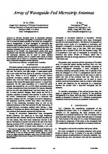
2. Structure and Design Fig.1 shows the structure of the single-layer slotted waveguide array antenna. The feeding waveguide is placed at the ends of the radiating waveguides on a single layer. Each radiating waveguide is fed by a coupling window. The coupling windows are spaced by a half guided wavelength in the feeding waveguide to excite 180-degree out-of-phase between adjacent radiating waveguides. The coupling of the windows is controlled by the width. Each radiating waveguide has a number of resonant slots. The coupling of the slots is adjusted mainly by the offset from the center axis of the waveguide. A feeding aperture is cut on the center of the feeding waveguide from the bottom. We design an 18 x 18-element array for uniform excitation at 94.0GHz [4]. The main beam is tilted by 4.7 degrees in the direction of the feed waveguide to suppress the reflection in the radiating waveguide. The width of the feeding waveguide and that of the radiating waveguide are 2.05mm and 2.10mm, respectively. The height of the waveguides is 1.00mm. The size of the antenna is 60mm x 55mm. Fig.1(b) shows the cross-section view of the antenna. The antenna requires basically only three types of layers or patterns for etching. They are for the slotted plate, the side walls for the feeding groove structure and the base plate with a feeding aperture. The lowest layer with the cross section of WR-10 standard waveguide with 3.5mm thickness is just for connecting a WR-10 waveguide by screwing for measurement. This layer is not required for a practical application. The step with 1.5mm thickness between the feeding aperture and the WR-10 waveguide in the cross section is for reducing the overall reflection. Each layer is laminated by several metal plates with 0.1mm thickness. In order to keep the shape of the antenna after diffusion bonding, we use 0.3mm thickness for the slotted plate, which is three times the conventional electrical dimension in the 25GHz
antenna, and 1.0mm thickness for the coupling windows, which is twice the conventional electrical dimension. The thickness for the side walls in the feeding groove structure is 0.5mm, which is equal to the electrical dimension in the 25GHz antenna. Large thickness of the side walls could increase the level of the second-order beams in the oblique cut planes due to the alternating-phase feed between adjacent radiating waveguides [5]. This level is acceptable for our design, which does not give serious degradation of the antenna gain. Fig.2 shows the offset and the length of the slots on the radiating waveguide for the thickness t of the slotted plate of 0.1mm and 0.3mm. The variation of the offset is identical between t=0.1mm and 0.3mm because all the slots are resonant and the coupling can be controlled even though the slotted plate is thick. We confirm that the reflection of the 18-slot array is less than -20dB over 90-98GHz both for t=0.1mm and 0.3mm. Fig.3 shows the division of a T-junction for the thickness d of the coupling window of 0.5mm and 1.0mm. The division for d=1.0mm has narrower bandwidth than that for d=0.5mm because the coupling windows narrower than the resonant width are cutoff and the field in the window region is exponentially decayed for large thickness. We also confirm that the 9-junction array for d=1.0mm has narrow bandwidth for the reflection below -20dB than that for d=0.5mm.
3. Experimental Results We fabricate the antenna by using two types of metal. One is stainless (SUS304) which is typically used for diffusion bonding because it is hard metal tolerable for high temperature of about 1000 degrees and high pressure in diffusion bonding. However the conductivity of stainless is low (1.4x10⁶ S/m) so that the conductor loss is large (0.226 dB/cm) in a WR10 waveguide at 94GHz. The other is copper where the conductivity is high (58.0x10⁶ S/m). The conductor loss of copper is still small (0.035 dB/cm) in a WR10 waveguide at a high frequency of 94GHz. However copper is soft in comparison with stainless so that the mechanical tolerance after diffusion bonding could be small. Fig.4 shows the picture of the antenna of copper. The size is 60mm long and 55mm wide. Fig.5 shows the near field distribution at 94.0GHz. In this figure, the feed waveguide is placed at the bottom and waves propagate from the bottom to the top in the radiating waveguides. In the phase distribution, the phase taper for the measured beam tilt of -5.4 degrees are subtracted. The amplitude is strong around the ends of the radiating waveguides. This could come from over etching of the slots. The phase is delayed toward the end of the radiating waveguide due to the over-etching slots. The phase is not symmetrical with respect to the center along the feed waveguide. This could be caused by the bending sidewalls of the radiating waveguide in the copper antenna after the diffusion bonding. Fig.6 shows the radiation patterns at 94.0 GHz. The main beam is tilted by -5.4 degrees in the H-plane. The highest sidelobe level is -9dB reflecting the tapered amplitude along the radiating waveguides as shown in Fig.5(a). The envelope of the sidelobes is not symmetrical in the E-plane. This comes from the asymmetric near field distribution in phase as shown in Fig.5(b). Fig.7 shows the reflection. The reflection of the copper antenna and the stainless one are -12dB and -8dB at 94GHz. The degradation is due to the misalignment of the thin metal plates in the diffusion bonding. Fig.8 shows the gain. The solid lines with marks indicate the gain simulated by HFSS including the conductor loss. The efficiency degrades due to the conductor loss. The solid line with circles indicates the measured directivity of the stainless antenna. Its peak is 78% at 93.0GHz. The solid line and the dashed line present the measured gain of the copper antenna and that of the stainless antenna, respectively. The peaks are 31.4dBi gain with 60% efficiency at 93.7GHz in the copper antenna and 30.0dBi with 44% efficiency at 92.2GHz in the stainless antenna. The antenna efficiency is expressed as the sum of the loss factors in dB by the following equation. (antenna efficiency) = (reflection loss) + (aperture efficiency) + (conductor loss) (in dB) Table 1 shows the loss factors of the both antenna. The aperture efficiency dominates in the copper antenna while the conductor loss dominates in the stainless antenna.
4. Conclusion We fabricate the single-layer slotted waveguide array antenna in 94GHz band by diffusion bonding of laminated thin metal plates. Low fabrication cost is expected because a die is not required
and a small number of the patterns etching the plates are used. A thicker plate of resonant slots and thicker coupling windows without resonances are required for the diffusion bonding. The former does not reduce the bandwidth of the radiating slot array while the latter decreases the bandwidth of the coupling windows. The copper antenna achieves 60% efficiency for 31.4dBi gain at 93.7GHz. The diffusion bonding could give the misalignment of the thin metal plates, which degrades the aperture efficiency. The efficiency will be enhanced after the aperture efficiency is improved.
References
1.6
0.4
1.5
0.3
1.3 1.2
0.2
offs et (t = 0.3mm) offs et (t = 0.1mm) 3
6
9 12 Slot Number n
15
0.1
0 18
Fig.2: Slot Parameters for the Thickness of the Slotted Plate
(a) overall view Slotted Plate (0.3mm)
0
Radiating Waveguide
Waveguide (1.0mm) 1.5mm (feed aperture) 3.5mm (WR10)
(b) cross-section view Fig.1: Single-Layer Slotted Waveguide Array Antenna
-3
-10
Reflection (dB)
Input Port 0.5l g T-junction
d = 1.0mm d = 0.5mm
-20
-4 -5
-30
-6
-40
-7
90
92
94 96 Frequency (GHz)
98
Fig.3: Division of a T-Junction for the Thickness of the Coupling Window
Transmission (dB)
Feed Waveguide
Base(5.0mm)
length (t = 0.3mm ) length (t = 0.1mm )
1.4
Offset p (mm)
Length l (mm)
[1] N.Goto, "A Planar Waveguide Slot Antenna of Single Layer Structure," IEICE Tech. Rept., AP8839, 1988. [2] N.Goto, "A Waveguide-Fed Printed Antenna," IEICE Tech. Rept., AP89-3, 1989. [3] R.C.Johnson and H.Jasik, “Antenna Engineering Handbook,” 2nd. Ed., Sec.9-6, McGraw-Hill, 1961. [4] M.Zhang, J.Hirokawa and M.Ando, “Design of Reflection Suppression and Aperture Field Distribution in the Waveguide Two-Dimensional Slot Array using Combination of Full-Wave MoM Analysis and Equivalent Circuit Model,” IEICE Tech. Rept., AP2007-112, 2007. [5] L.Kurtz and J.Yee, “Second-Order Beams of Two-Dimensional Slot Arrays,” IEEE Trans. Antennas Propagat., vol.5, no.4, pp.356-362, 1957.
Relative Amplitude (dB)
0 -10
E-plane
H-plane
-20 -30 -40 -90
-60
-30 0 30 60 Angle (deg) Fig.6: Radiation Patterns (94.0GHz)
90
0
Fig.4: Picture of the Diffusion Bonding Antenna of Copper 30
0 -2 -4 -6
10
-15 -20
90
92
94 Frequency (GHz) Fig.7: Reflection
-8
0
-10 -12 -14 -16 -18 -20
-10 -20 -30 -30 -20 -10
0
10
20
30
180 150 120 90 60 30 0 -30 -60 -90 -120 -150 -180
20 10 0 -10 -20 -30 -30 -20 -10
0
10
20
HFSS (PEC) HFSS (SUS304) HFSS (copper)
30
x position (mm) (b) Phase (degree) Fig.5: Near Field Distribution (94.0GHz)
SUS304 Copper HFSS 96 98
Directivity Gain (SUS304) Gain (copper)
34 90% 80% 32 70%
30
x position (mm) (a) Amplitude (dB)
y position (mm)
-10
-25
Gain (dBi)
y position (mm)
20
Reflection (dB)
-5
30
50% 40%
28 30% 26 90
92
94 96 Frequency (GHz)
Fig.8: Gain Table 1: Loss Factors Copper Stainless Reflection loss -0.27dB -0.31dB Aperture efficiency -1.61dB -1.14dB Conductor loss -0.34dB -2.12dB Antenna efficiency -2.22dB -3.57dB
98