switches based on decoding/multiplexing architecture, this chip utilizes a routing ... Paths are passive and bi-directional so performance varies according to the ...
A 1024 PIN UNIVERSAL INTERCONNECT ARRAY WITH ROUTING ARCHITECTURE
Richard Guo, Hung Nguyen Adi Srinivasan , Henry Verheyen , Hong Cai , Steve Law, Amr Mohsen
APTIX 225 Charcot Ave , San Jose, CA 95131 Phone: 408-428-6200
Abstract
Chip Architecture
A re-programmable , universal interconnect array, with 1024 pins and over 1 million transistors is fabricated with 0 . 8 ~triplemetal CMOS technology. Unlike the conventional cross-point switches based on decoding/multiplexing architecture, this chip utilizes a routing architecture which allows an order of magnitude higher pin connectivity with random connections of any number of pins to any other pin. Paths are passive and bidirectional with typical pin-to- piadelay of less than 7NS. This chip also supports optional battery backup.
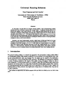
Introduction Crosspoint switch ICs have been widely used in applications such as real-time reconfigurable system, PBXs , parallelprocessing, test interfaces, industrial-control-routing, and datacommunications systems. Other applications utilize the crosspoint switch to change functionality of a circuit by altering the interconnect between board-level components , for example in ASIC emulators with multiple FPGA devices. Prior analog and digital implementations of crosspoint switch ICs have utilized a decoding/multiplexing architecture as shown in Figure 1. The number of circuits and chip area of such an architecture implementation increase rapidly with the product of the number of input and output lines. Numerous crosspoint switches are avilable for analog and digital signals having from 8 lines ( 4 input and 4 output ) to 128 lines ( 64 input and 64 output ). This paper describes a single-chip, re-programmable , universal interconnect array utilizing a novel routing architecture which provides an order of magnitude higher pin connectivity than the conventional decoding architecture. This chip has 1024 pins and over one million transistors fabricated with 0 . 8 ~triple-metal CMOS technology. Unlike conventional crosspoint switches, this chip allows any number of pins to beconnected to any other pin. Paths are passive and bi-directional so performance varies according to the speed and strength of the driving circuit. Retention of the programming data is accomplished with conventional SRAM technology.
In order to accommodate 1024 pins efficiently, the chip is organized in an array of 32 X 32 pins. The chip architecture is shown in Figure2. Between the rows and columns of pins the array contains horizontal and vertical interconnect channels respectively. The channels consists of a set of segmented tracks that span the full width of the array. Each pin has anL shaped pin stub which spans one row and one column. This minimizes the base capacitance at a Pad, while ensuring that it can be connected to any other Pad by the use of 3 or less switches in series. The metal paths along each track are a mix of long and short segments which let a single track be used in more than one link whenit has a break in between. Switchcells are located at the intersection of the segmented tracks. The population density of the switch cells, number of tracks per channel and the average segment length are optimized for performance, cost, and routability. Pin stub switches have twice the size compared to the normal segment switches since the probability for k i n g chosen for the former ones is much higher than the latter ones. The switches between long segments also have larger size versus those between short ones to achieve tighter speed distribution between worst case and best case delay. The circuit diagram of the switch cell is shown in Figure 3. The switch cell consists of a specially designed RAM cell with built-in level shifter and a NMOS pass transistor. The drain and source terminals of the NMOS pass transistor are connected to vertical or hiorizontal tracks and the gate is driven by the RAM cell. For the case of "open" the ram cell stores a "0" , and for the case of "short" the ram cell stores a "1". In order to have full VCC signal and cut down the ON resistance, the gate of each NMOS pass transistor is driven by the voltage level VPP, which is higher than VCC and is derived from an internal charge pump. This approach combined with special router software which generates shortest possible connection between pins, yields a typical pin to pin resistance of 120 ohm to 150 ohm, and capacitance of 35pf to 45pf depending on fanout. We also found from simulation that U0 buffers were not needed even for the case with large I/O loading due to the extra delay caused by IlO buffers itself. The key characteristics of this chip are listed in Table 1.
4.5.1 IEEE 1992 CUSTOM INTEGRATED CIRCUITS CONFERENCE
0-7803-0246-x/92 $3.00
1992 IEEE
Pin
Output Port
Switch cell
-+=$+LE+ & Logi
Decoding & Multiplexing Circuits
Figure 1 -- Prior DecodinglMultiplexing Architectures of Crossooint Switch ICs Figure 2
-- Novel Routing Architecture for the Universal Interconnect A r r a y
The RAM cell has separate read and write path to the bit-line to insure the cell stability during the " read " and also improve the "write" margin. The bit-line and word-line are drivcn by corresponding bit-line and word-line shift registers. During "read" bit-line sensing output is loaded back into the same bitline shift registers through the feedback path. The level shifter of the RAM cell improves the margin for high voltage breakdown or snap back. At the initial power up state, all the Ram cells must be in the '0' state in order to keep all the pass gate off. Internal power up circuitry guarantee all bit-lincs and word-lines are turned on to write '0 state into every Ram cell during power-up. The VPP charge pump must be designed to be strong enough to override all thc sub Vt leakage, junction leakage and switching current of RAM cell during the programming and normal operation. This chip uses a back bias-generator to reduce the parasitic capacitances and improves latch-up immunity. This chip also supports battery backup application due to it's low standby currcnt (