FPGA placement determines the location of logic blocks ... 3) Fixed, as well as programmable, routing resources used to realize all required ...... To intensify the exploration of the problem space, SA employs a double loop. ...... [10] C. Blum and A. Roli, âMetaheuristics in combinatorial optimization: Overview and conceptual ...
1
A Comparison of Heuristics for FPGA Placement S. Areibi and X. Bao School of Engineering G. Grewal, D. Banerji and P. Du Department of Computing & Information Science University of Guelph, Guelph, Ontario Canada N1G 2W1
Abstract Field-Programmable Gate Arrays (FPGAs) are digital integrated circuits (ICs) that contain configurable logic and interconnect to provide a means for fast prototyping and also for a cost-effective chip design. The innovative development of FPGAs spurred the invention of a new field in which many different hardware algorithms could execute on a single device [16]. Efficient Computer Aided Design (CAD) tools are required to compile hardware descriptions into bit-stream files that are used to configure the target FPGA to implement the desired circuits. Currently, the compile time, which is dominated by placement and routing phases, can easily take hours or even days to complete for current large (over 8-million gate) FPGAs. Within the next few years the logic capacity of FPGAs will tend to increase dramatically (up to 40-million gates) that prohibitively long compile times may adversely affect instant manufacturability of FPGAs and become intolerable to users seeking very high speed compile. This paper presents several constructive and iterative improvement placement based heuristics that significantly reduce the amount of computation time required to achieve high-quality placements, compared with VPR [9], [8]. Cluster Seed, GRASP and Partitioning based approaches prove to be excellent candidates to generate good starting points in negligible amounts of time. The effectiveness of these constructive based methods are tested by implementing several local search based methods. Meta-heuristics in the form of Tabu Search and a hybrid Simulated Annealing with short-term memory are further implemented to explore and exploit the solution space effectively.
Keywords — FPGA Placement, GRASP, Cluster Seed, Partitioning, Simple Local Search, Tabu Search, Simulated Annealing with Memory I. I NTRODUCTION An FPGA has become a popular means to realise digital systems because of its dramatic reduction of turn-around time and start-up cost compared with traditional Application Specific Integrated Circuits (ASICs). FPGA placement and routing are two critical phases in FPGA design. FPGA placement determines the location of logic blocks required by circuits in the chip such that the area and speed are optimized. The quality of placement greatly affects the routing phase. Once placement is completed, routing is performed by assigning the actual interconnections between logic blocks. Due to the fact that both placement and routing are NP-hard [30], both phases of design can consume most of the CPU time during compilation. Current CAD tools provide high-quality placement and routing solutions at the expense of CPU time [25]. The compile time tends to increase tremendously as the size of circuits becomes larger. With the continuous increase in the logic capacity of FPGAs, it is imperative to develop effective and efficient placement and routing algorithms that will provide acceptable solutions in reasonable amounts of CPU time. Also, as we move to sub-micron designs, circuit delay, as well as power dissipation [2] are mostly caused by the interconnections among logic elements [27]. This problem is especially severe for FPGAs, which employ programmable switches and connections instead of metal lines to implement a net-list. Poor solutions, even derived quickly, are often not acceptable in industry. With 40-million gate FPGAs on the horizon, these prohibitively long compilations may nullify the time-to-market advantage of FPGAs. Therefore, there is a great need for CAD tools that execute in a reasonable amount of CPU time, while still generating high-quality solutions. In this paper, we focus on the placement phase of the FPGA-based design process, with the goal of reducing the compile time to achieve high-quality placements. The most important goal for FPGA placement, minimizing the total wire-length required to complete the routing, is used as our placement objective. Several iterative improvement/metaheuristic placement algorithms are provided which dramatically reduce compile times, while still achieving highquality placements. Local search iterative improvement techniques [6] are implemented to obtain good solutions in very short periods of time. The first is Simple Local Search (SLS) which uses a general iterative improvement strategy. SLS attempts to achieve reduction in wire-length cost by swapping blocks in a window which limits
2
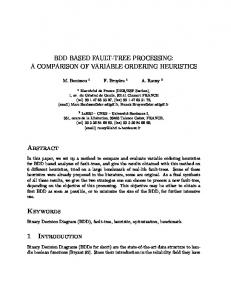
the swapping region. Initially the window is large, and as the heuristic progresses the window shrinks in size. Local search is also implemented as an Immediate Neighbourhood Local Search (INLS). This technique is capable of obtaining reasonable quality placements fast by swapping adjacent blocks surrounding the selected blocks. Furthermore, several meta-heuristics are implemented to further improve solution quality by effectively exploring the solution space. Tabu Search (TS) attempts to efficiently explore the solution space utilizing memory as a mechanism to avoid getting stuck at a local optimal. Finally an adaptive placement algorithm, called Greedy Simulated Annealing (GSA), which employs a short-term memory to record recent search history is investigated. This information is used in an unique way to improve the convergence rate of the traditionally slow Simulated Annealing (SA) algorithm. The overall effect is a significant reduction in time to obtain high-quality placements compared with other SA-based techniques, such as VPR [7]. A. Contributions and Paper Organisation The main contributions of this paper can be summarised as following: (i) Development and implementation of several constructive based placement techniques (Cluster Seed, GRASP, Partitioning Based) and investigating their effectiveness in terms of solution quality and CPU time, (ii) A thorough investigation of the performance of several meta-heuristic search techniques for FPGA placement, (iii) Introducing a hybrid search technique GSA which combines certain features from Tabu Search and Simulated Annealing. The remainder of this paper is organised as follows: Section II presents related work and necessary background material. Section III describes constructive based approaches in the form of Cluster Seed Search, GRASP and multiway partitioning. Section IV presents several local search techniques in the form of Simple Local Search (SLS) and Immediate Neighbourhood Local Search (INLS). Several Meta-heuristic and hybrid techniques are presented in Section V. In Section VI, we compare the results obtained using both of our new heuristics with those obtained by VPR. Finally, conclusions and future work are presented in Section VII. II. BACKGROUND There is a wide variety of architectures for FPGAs from different vendors including Xilinx, Altera, Lattice, Actel and QuickLogic. Although the exact structure of these FPGAs varies from each other, all FPGAs consist of three fundamental components as shown in Figure 1: 1) Logic blocks that are capable of implementing combinational/sequential logic functions; 2) I/O blocks or I/O pads for communication with the outside world; and, 3) Fixed, as well as programmable, routing resources used to realize all required inter-connections between the blocks. Vertical Routing Channel
Switch Box
IO blocks
CLB
CLB
CLB
CLB
CLB
CLB
CLB
CLB
CLB
Configurable Logic Blocks
. .
Horizontal Routing Channel
Fig. 1.
An Island Based FPGA Architecture
The Island Style FPGA architecture is employed by many vendors [33]. Logic blocks in this architecture are referred to as Configurable Logic Blocks (CLBs) and arranged as a symmetrical array. Routing tracks have Manhattan geometry; that is, they are either horizontal or vertical. The detailed routing structure consists of three components: connection blocks, switch blocks, and routing channels. A connection block is used to connect a CLB to the routing channels via programmable connections. The pins of each CLB pass uninterrupted through the connection block and have the option of “fusing” to some channel segments. The switch block is a switch matrix that is used to connect wires in one channel segment to other wires.
3
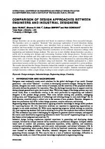
Depending on the topology [33], each wiring segment on one side of a switch block may be connected to some or all of the wiring segments on the other three sides. This flexible routing structure enables every CLB to have connections with any other CLB or I/O pad, depending on the number of tracks in the routing channels. A CLB in most commercial FPGAs consists of one or more Basic Logic Elements (BLE). Each BLE usually consists of a Look Up Table (LUT) and a register. A. FPGA Placement FPGA placement usually begins with a net-list of logic blocks, which includes CLBs and I/O pads, and their interconnections. The result of placement is the physical assignment of all blocks and pads on the target FPGA, as shown in Figure 2, that minimises one or more specific objective cost functions (wire-length, speed, power dissipation, etc.). In order for an FPGA to accommodate the design, some void (unused) CLBs and pads are usually present. Place blocks to FPGA
Initial CLBs and I/O pads after Packing 0
1
2
3
4
5
6
7
0
1
2
3
4
5
6
7
8
9
Pad array Void blocks
0 1 2 3 4 5 6 7 v0 (1,2) (3,1) (1,3) (2,1) (1,1) (2,3) (3,3) (2,2) (3,2) 0 1 2 3 4 5 6 7 8 9 v0 v1 (4,1) (0,1) (0,3) (2,4) (4,3) (2,0) (3,0) (1,4) (3,4) (1,0) (0,2) (4,2)
Representation of CLBs and I/O pads after Placement Fig. 2.
7 (1,4)
3 (2,4)
8 (3,4)
2 (0,3)
2 (1,3)
5 (2,3)
6 (3,3)
4 (4,3)
v0 (0,2)
0 (1,2)
7 (2,2)
v0 (3,2)
v1 (4,2)
1 (0,1)
4 (1,1)
3 (2,1)
1 (3,1)
0 (4,1)
9 (1,0)
5 (2,0)
6 (3,0)
CLB array
FPGA coordinate system
Example of a placement for FPGA.
The most basic objective for FPGA placement is to minimise the routing cost, which is the total wire-length required to complete the routing. Routing cost is used because reducing it actually reduces a number of associated design parameters. By reducing the routing length, the routing resources required by all interconnections are also reduced. This results in an increase in circuit speed due to the reduction in connection capacitance and resistance. Power consumption, which is another very important parameter to measure the quality of an FPGA implementation, is reduced too [27]. If the objective of the placement tool is to minimise the routing cost, the process is referred to as wire-length-driven placement. There are other objective terms that can be added to the original cost function to directly optimise the various design goals [28]. For example, placement can be performed to minimise the length of a critical path to meet timing constraints, referred to as timing-driven placement [23] [32], or to balance the wire density across the FPGA device, referred to as routability-driven placement [26]. In this paper, we use the wirelength-driven approach as a metric in our FPGA placement approach. In the placement phase, it is computationally too expensive to determine the exact configurations of routing resources to realize physical connections for CLBs and I/O pads, which actually is another N P -hard problem. For this reason, the routing cost is approximated during placement. The speed and accuracy of estimation have a significant effect on the performance of any placement tool. The Half-Perimeter Wire-Length (HPWL) model is the most widely used method to estimate the wire-length of a net [31]. A net is approximated by half the perimeter of the smallest bounding rectangle that encloses all terminals in the net, as shown in Figure 3. In a Manhattan routing structure, the HPWL of a net approximates the length of a Steiner tree, which is the lowest bound on the final routing cost on a net. Given a block b with coordinates (x b , yb ), the half-perimeter of net i is calculated as follows: HP W Li = (M AXb∈i {xb } − M INb∈i {xb } + 1) + (M AXb∈i {yb } − M INb∈i {yb } + 1)
(1)
For a net with two or three terminals, the routing cost obtained by HPWL model is accurate. When there are more than three terminals in a net, a q(i) factor [11] is introduced to compensate for the fact that the HPWL model under-estimates the wire-length necessary to connect all blocks. The value of q(i) depends on the number of terminals in net i. The parameter q(i) is 1 for nets with 3 or fewer terminals, and gradually increases to 2.79
4
(Xmax, Ymax)
Bounding Box
(Xmin, Ymin) HPWL Fig. 3.
Half-perimeter wire-length model
for nets with 50 terminals. For exceptionally heavy fanout nets that have more than 50 terminals, the value of q(i) increases linearly [8] at the rate of: q(i) = 2.7933 + 0.02616 ∗ (T erminalN umber − 50)
(2)
Therefore, the final cost function, called the bounding box cost, takes the following form: Costbounding
box
=
NX nets
q(i) ∗ HP W Li
(3)
i=1
Consequently, the FPGA placement pertaining to this paper is equivalent to the problem of minimizing the bounding box cost. B. Previous Techniques for FPGA Placement FPGA placement is an N P -hard combinatorial optimisation problem, hence no polynomial-time algorithm is known to produce an exact solution [31]. In recent years, many heuristic techniques have been developed in an attempt to obtain (sub-optimal) solutions in a reasonable amount of time. Historically, these methods have been divided into two classes: partitioning-based placement [18], [5] and iterative improvement [7], [9]. In partitioning-based placement, a circuit is recursively bi-sected, minimizing the number of cuts of the nets that connect components between partitions, while leaving highly-connected blocks in one partition. Eventually, the partition size reaches a few blocks to obtain improvement by grouping the highly-connected blocks together. These kind of methods are good from a “global” perspective, but they do not directly attempt to minimise wire-length. Therefore, the solutions obtained are sub-optimal in terms of wire-length. However, they run fast, and are normally used in conjunction with other search techniques, such as local search, for further quality improvement. Iterative improvement methods start with an initial placement and seek improvements by searching for small perturbations in the neighbourhood of the placement that results in better solutions. For FPGA placement, these perturbations are location swaps (pairwise move) between two blocks (either two CLBs or two I/O pads). In local search methods [1], only the moves that will improve the current solution are accepted. Placement heuristics in this category can run fast if well implemented. The weakness of these methods is related to the fact that they can easily get trapped in local minima. When the number of local minima is large, which actually seems to be a generic feature of many of the classic N P -hard problems including placement [4], the probability that these heuristics converge to a global minima is extremely small. Meta-Heuristics, in the form of Simulated Annealing (SA), improve the performance of basic local search by allowing hill-climbing (i.e., accepting moves that would deteriorate the objective function) to escape local optima, which usually cause the latter heuristic to terminate. Besides accepting beneficial swaps, moves that deteriorate the solution will be accepted in SA with a probability of e−∆C/T , where ∆C is the change in cost, and T is analogous to temperature in the metal crystallisation process. The changes of T is referred to as annealing schedule. Initially, T is set to a high value such that most inferior solutions can be accepted. As the annealing process continues, T gradually decreases (cooling), reducing the probability of accepting poor solutions. In the final stage, T usually is only a small fraction of its original value and almost only improving solutions are allowed. Currently, SA-based
5
placement heuristics, like VPR [7], [9], have achieved similar or higher quality solutions, compared to other types of placement tools. However, this improvement often comes at the expence of longer runtime [24]. A more recent approach is to reduce the complexity of large circuits by clustering them into less complicated and easily solvable forms, which helps to decrease the time required to obtain good solutions for the overall problem. This approach has been applied successfully to circuit partitioning [19] and VLSI standard-cell placement [3]. In many cases, a decrease in computation time by an order of magnitude compared to manipulating the flat net-list is reported [3], [19]. Only recently has this approach been applied to the FPGA placement problem [29], and then only in a limited way. C. FPGA Benchmarks Ten MCNC [34] benchmark, shown in Table I, are used to measure the performance of all heuristics developed in this paper1 . This suite consists of circuits ranging from a few hundred CLBs to nearly ten thousand CLBs and is organised into three groups: small, medium and large. The “FPGA matrix” column is the actual CLB matrix of target FPGA, which is the minimum size to hold the design. In our approach, an island style FPGA model, with each CLB containing a single 4-input lookup table (4-LUT) and a single D flip-flop is used. The I/O pad pitch-to-logic block ratio[7], which is the number of pads available at each marginal block location, is set to 2. Each CLB has 6 pins: 4 inputs, 1 output, and 1 clock (global), and we assume the FPGA has dedicated resources for routing the clock, reset and other global nets. Circuit name e64 tseng ex5p alu4 seq frisc spla ex1010 s38584.1 clma
FPGA matrix 17x17 33x33 33x33 40x40 42x42 60x60 61x61 68x68 81x81 92x92
Number of CLBs 274 1047 1064 1522 1750 3556 3690 4598 6447 8383
Number of I/O Pads 130 174 71 22 76 136 62 20 342 144
Number of nets 290 1099 1072 1536 1791 3576 3706 4608 6485 8445
Average fanout 3.94 4.28 4.73 4.52 4.46 4.48 4.73 4.49 4.18 4.61
TABLE I MCNC B ENCHMARK CIRCUIT SUITE USED AS TEST CASES
III. C ONSTRUCTIVE BASED T ECHNIQUES Constructive placement techniques are excellent candidates to generate good starting points in negligible amounts of time. These techniques have been successfully applied in ASIC design [36]. In traditional constructive placement, a seed cell is chosen and placed within the layout of the chip. Next, a cell is picked up from a pool of unused cells (according to their connectivity to the previously placed cell) and placed in an empty position near the initial seed cell. This process is repeated until a legal placement solution is obtained. Several constructive based techniques are investigated in this section based on (i) Cluster Seed, (ii) GRASP, and (iii) Partitioning Based Approach. A. Cluster Seed Search Cluster Seed Search (CSS) is a constructive (cluster growth) based approach used to build up an initial and legal placement. Cluster growth placement techniques have been successfully applied to standard cell design [35]. They are considered as bottom-up methods that operate by choosing cells and placing them into a partial placement [4]. There are two main functions used by cluster growth: (i) selection function and (ii) placement function. The selection function is responsible for selecting the best candidate based on a connectivity metric. The placement function decides the best location for the cells according to the availability of vacant space in the area [4]. In traditional ASIC standard cell placement [36], constructive algorithms are generally based on primitive connectivity rules. Cell arrangement is based on the degree of connectivity to the previously placed cells (most densely connected first) [30]. However, since the number of input and output pins of each logic block is fixed, connectivity rules for traditional ASIC design do not perform as well for FPGA design. Therefore in the FPGA 1 Most
researchers use the benchmarks to validate their results
6
c2 Seed Cell
c1
c1
c3
c4 c2
c3 c4 (a)
l2 Seed CLB
l1
l1
l4
l2 l3
l3 l4
(b)
Fig. 4.
CSS in (a) Standard Cell Design and in (b) FPGA design
placement, CSS uses the fanout number as a criterion to select the best block and create an improved initial and legal placement solution. A logic block with high fanout indicates that this block belongs to a net which has more terminals. Moving these logic blocks with high fanout together tends to shrink the bounding box of the net containing more terminals with higher probability. Figure 4 illustrates the difference of CSS in standard cell design and FPGA design. In Figure 4 (a), c1 has higher physical connectivity to c3 than c2 and c4 , and therefore c3 is placed closer to the seed cell c1 . However in Figure 4 (b), l4 has a higher fanout than l2 and l3 , and accordingly l4 is placed to the location closest to the seed CLB l1 . The pseudo-code for CSS is shown in Figure 5. Typically, a seed block is selected randomly and placed on the FPGA fabric. The next block is then chosen from the remaining unplaced blocks which are connected to the previously placed seed block based on their fanout. The latter is placed at a vacant location closest to the seed block, such that the wire-length is minimised. This current placed block becomes the next seed for next selection. The process is repeated until an improved initial and legal solution is constructed.
1. Seed = RandomSelectSeed(); /*randomly pick a block as a seed*/ 2. SetLocationOfSeed(); /*place random seed at the first position of FPGA*/ 3. While(Initial Solution Not Complete) 4. { CreateListOfFanoutNumber(Seed); /* create the list of fanout number of blocks connected to the seed*/ 5. Seed = SelectBestBlock(); /*select the block with the highest fanout number as the next seed*/ 6. SetLocationOf Seed(); /*place current seed at the location close to the previously placed seed*/ 7. } /* end of loop */ 8. Return the solution Fig. 5.
Pseudo-code for CSS
B. GRASP The GRASP meta-heuristic is a multi-start or iterative process, in which each iteration consists of a construction phase followed by a local search phase [14]. Normally, an initial and feasible solution is built up in the constructive phase. A local improving process follows up to explore the neighbourhood of this initial solution and attempts to iteratively improve it. The best solution found in the iteration is stored as the final result. As a constructive based technique, GRASP has two main parameters that need tuning. The first is the stopping criteria, and the second is
7
the element selection method in the restricted candidate list. Since only a few parameters need to be tuned, this makes GRASP appealing to researchers.
for i = 1 to Max Iteration do { S = InitializationForConstruction(Seed); /*randomly pick up a pad and put all CLBs at the location closest to it*/ 3. EvaluateInitialBBCost(S); /*calculate the bounding box cost of this infeasible solution*/ 4. while ( Initial Solution contruction (S) not done ) { 5. CreateCandidateList(RCL); /*greedily create candidate list according to bounding box */ 6. TargetBlock = SelectBestBlock(RCL); /*select from RCL a block which will cause least increase in HPWL */ 7. S = SetBestBlock(TargetBlock); /*place selected best block close to the previous target block*/ 8. ReevaluateBBCost(S); /*recalculate the bounding box cost of the partial solution*/ 9. } repeat if a legal initial solution is not created yet 10. } /*end of for*/ 1. 2.
Fig. 6.
GRASP Pseudo-code for FPGA Placement
The pseudo-code in Figure 6 illustrates the GRASP algorithm. The parameter Max Iteration is the number of iterations executed and Seed is used as the initial point for the construction of the solution in each iteration. In the current implementation, I/O pads are randomly distributed around the FPGA chip and an I/O pad is selected as Seed in each iteration. Initialisation and Evaluation of Partial Solution Unlike generic GRASP implementations, GRASP for FPGA placement starts with a partial solution instead of an empty solution in each iteration, as shown in Figure 7(a). At first, I/O pads are randomly placed around the FPGA chip, and their locations are not changed during the construction phase. Next, an I/O pad is chosen randomly as the initial Seed for the construction process. Meanwhile, all the CLBs are placed at the closest location to the initial Seed. These CLBs are moved, based on a greedy function, until a legal complete placement solution is generated. Construction Phase At each iteration of the construction phase, a set of candidate CLBs is chosen to be added to the partial solution. While a CLB is incorporated into the partial solution under construction, the incremental increase in wire-length cost of the new solution is usually represented by the greedy function. The evaluation of all unplaced CLBs by this function leads to the formation of a restricted candidate list (RCL), as shown in Figure 7(b). A CLB that results in the smallest incremental wire-length is selected to be placed to the closest location to the previously placed target CLB2 . Once the best CLB is added to the partial solution, it is removed from the candidate list. The process is repeated until the construction phase is completed. C. Partitioning Based FPGA Placement Partitioning based methods, also referred to as min-cut techniques, have been successfully applied in several areas (e.g., VLSI design automation, parallel processing, data mining and efficient storage of large databases on disks). Iterative improvement methods used in the past are based on Fiduccia-Mattheyses (FM) algorithm [15] and the Kernighan-Lin (KL) algorithm [20]. The partitioning based FPGA Placement presented in this section starts by randomly dividing the circuit into two blocks. The partitioning algorithm is then applied to minimise the number of nets cut between the two partitions. This is applied in a recursive manner until each partition contains a few blocks that are highly-connected. Figure 8 shows the mechanism by which the algorithm (either simple iterative or based on a meta-heuristic) swaps two blocks to reduce the wire-length cost. 2 Notice
that either location (1,2) or (2,3) would be suitable to the CLB placed in location (1,3).
8
0 0
Seed 3
1 1
2
3
4
5
2
3
4
5
v
5
v
(1,4)
(2,4)
(3,4)
01....6
(0,3)
1 (0,1)
(1,0)
0
I/O pads array
(0,3)
v
v
v
(2,3)
(3,3)
(4,3)
v
v
4
(2,2)
(3,2)
(4,2)
v
v
v
v
(1,1)
(2,1)
(3,1)
(4,1)
0
v
2
(1,0)
(2,0)
(3,0)
2
3
4
Location in FPGA chip
. 3
CLB
(0,3)
5
1
2
3
I/O pads array
(2,4)
4
5
6
CLBs array
(0,3) (0,3) (0,3) (0,3) (0,3) (0,3)
0
6
4
1
3
2
20
35
64
75
80
93
Next placed location
I/O pad
v (1,2)
1
(0,1) (3,0) (0,3) (4,2)
v (2,3)
Void Block
(1,3)
v (0,2)
0
CLBs array
6
0 (0,3)
1
2
3
4
5
6
CLBs array
1
(0,3) (0,3) (0,3) (0,3) (0,3) (0,3)
(0,1)
0 (1,0)
1
2
3
4
(0,1) (3,0) (0,3) (4,2)
5
I/O pads array
(2,4)
CLBs
RCL
99
Incremental cost
v
5
v
(1,4)
(2,4)
(3,4)
12......6
0
v
v
(2,3)
(3,3)
(4,3)
Void Block
I/O pad
(1,3)
v (0,2)
5
v
v
v
4
(1,2)
(2,2)
(3,2)
(4,2)
v
v
v
v
(1,1)
(2,1)
(3,1)
(4,1)
0
v
2
(1,0)
(2,0)
(3,0)
Location in FPGA chip
.
CLB
Initial representation of CLBs and I/O pads for the construction
(a) GRASP Construction Phase Fig. 7.
(b) GRASP: RCL Construction
GRASP: Construction Phase/RCL Construction
new partitions
(b)
(a)
Blocks that are located in different partitions are picked to be swapped Fig. 8.
Partitioning Based FPGA Placement
D. Constructive Techniques: A Comparison The performance of the different constructive based techniques discussed for FPGA placement are compared based on the ten MCNC benchmarks. The comparison is made in terms of solution quality (total wire-length) achieved by each method and the CPU runtime. The Partitioning-based algorithms CSS and GRASP are run to create initial solutions. The Partitioning-based algorithm is carried out based on the simple local search (SLS) that is introduced in Section IV-A. Table II shows results obtained by running these algorithms 10 times. Although the results obtained by CSS are inferior, it achieves 19% average improvement over the random based approach in a short time. Partitioning-based algorithm achieves the best results with 44% average improvement compared to random based placement. GRASP yields 25% improvement over randomly generated solutions but suffers from larger CPU time overhead. Table III shows the results obtained using several constructive based techniques followed by an iterative improvement phase (based on INLS3 introduced in Section IV) to further enhance the solution quality. GRASP based on INLS achieves on average 12% improvement compared to Random + INLS. The CSS constructive based method achieves on average 5% improvement. The partitioning based algorithm combined with INLS on the other hand achieves on average 11% improvement. 3 INLS
refers to Immediate Neighbourhood Local Search.
9
Circuit name
Avg.random initial cost
e64 tseng ex5p alu4 seq M.avg frisc spla ex1010 s38584.1 clma L.avg Avg
7542 41286 42301 61504 79903 46489 229152 236251 332664 559870 796591 430905 238697
Partition-F Avg. Avg.CPU cost runtime(s) 5074 0.1 20293 0.4 22392 0.5 37291 1.8 52190 1.9 33042 1.2 119272 4.3 128432 4.3 192384 5.8 286332 7.5 459302 11.4 237104 6.7 132276 3.8
GRASP-F Avg. Avg.CPU cost runtime(s) 6451 0.05 30579 0.7 33854 0.6 48711 1.4 63513 1.8 44164 1.1 165651 6.7 161950 7.8 245879 10 415661 22 613427 36 320513 16 178567 8.7
CSS-F Avg Avg.CPU cost runtime(s) 6992 0.01 34808 0.05 37381 0.04 53175 0.08 69390 0.11 48688 0.07 177393 0.44 181525 0.47 264977 0.74 478670 1.33 631368 2.20 346786 1.03 193567 0.54
TABLE II C OMPARISON BETWEEN PARTITIONING , CSS AND GRASP WITH R ANDOM I NITIAL S OLUTIONS
Circuit Random-INLS-F GRASP-INLS-F name Avg. Avg. Avg. Avg. cost time(s) cost time(s) e64 4004 0.04 3589 0.05 tseng 15803 0.23 13933 0.53 ex5p 21352 0.24 19858 0.6 alu4 28635 0.35 25160 1.22 seq 39096 0.50 35610 1.45 M.avg 26221 0.33 23640 0.9 frisc 102901 1.28 92581 5.5 spla 110372 1.38 98455 5.95 ex1010 138479 3.0 108885 8.8 s38584.1 204574 3.62 183201 20.1 clma 330038 6.07 297464 35.6 L.avg 177272 3.07 156117 15.1 Avg 99575 1.61 87873 7.9
Partition-INLS-F Avg. Avg. cost time(s) 4001 0.12 14473 0.44 20061 0.51 26097 1.9 36671 2.1 24325 1.3 93088 4.6 95641 4.9 111177 6.4 183297 9.1 301505 13.9 156941 7.8 88602 4.4
CSS-INLS-F Avg Avg. cost time(s) 3905 0.02 15729 0.18 20445 0.22 27517 0.27 37174 0.36 25216 0.26 94450 1.04 101296 1.65 128115 3.72 194362 3.94 318885 6.14 167421 3.31 94180 1.76
TABLE III A
COMPARISON BETWEEN
PARTITION /CSS/GRASP WITH INLS
IV. L OCAL S EARCH T ECHNIQUES As one of the most basic iterative heuristic methods, local search algorithms can find approximate solutions to large-scale combinatorial optimisation problems [1]. The fundamental principle underlying a local search algorithm is that it always moves from the current solution to the next improving solution within the neighbourhood in a greedy manner. Local search algorithms attempt to improve the solution quality either stochastically or deterministically. The stochastic strategy always accepts the first improving solution found during random evaluation. The deterministic strategy on the other hand scans and evaluates the whole neighbourhood and accepts the best available solution. Typically, local search techniques terminate either by getting stuck in a local minimum or after a predefined number of iterations have passed. A. Simple Local Search (SLS) Simple Local Search uses a simple iterative improvement strategy that swaps blocks in a window which limits the region for swapping as shown in Figure 9. Initially the window is set to some large value, usually spanning the whole FPGA chip to enable the exploration of the solution space. As the algorithm progresses, the window shrinks in size to finely tune the search (i.e., enable fine-tuned search). In the current search window, two blocks are randomly selected and evaluated; the swap of these blocks is accepted if the wire-length cost is reduced. The number of iterations is defined by the following equation: Niterations = 10 × (Nblocks )1.33
(4)
where Nblocks is the total number of CLBs and I/O pads. By starting from an initial legal solution, searching the whole neighbourhood consumes considerable time which is prohibitively large for NP-hard problems, while
10
FPGA Chip
Initial search window size
Final search window size
Fig. 9.
. .
. .
The Search Window of SLS
attempting to achieve improvements. The pseudo-code for this strategy is shown in Figure 10. The complexity of the algorithm is of order O(n) where n is the number of iterations. Since SLS uses a non-deterministic strategy to move from the current solution to a neighbouring solution, it attempts to accept the first improving solution. Although this stochastic strategy makes local search algorithms run fast, it prevents the latter from aggressively finding the best solution in the neighbourhood. This may easily trap the heuristic in sub-optimal solutions that are far away from the global optimal.
1. SetExitCriteria(); /*set iteration number*/ 2. S = InitialPlacement(); /*create the initial solution*/ 3. window = SetToWholeChip; 4. set Niteraion ; 5. while(Niteraion != 0) /*start of loop*/ 6. { Block1 = RandomSelectBlock(window); /*randomly pick up the first block*/ 7. Block2 = RandomSelectBlock(window); /*random pick up the second block*/ 8. C = Cost(Block1) - Cost(Block2); /*calculate the change of cost if swapping these two blocks*/ 9. if(∆C < 0) /*only accept the improving swaps*/ 10. S = SwapPosition(Block1,Block2); 11. Niteraion = Niteraion -1; 12. window = UpdateWindow(Niteretions ); /*update the size of the search window*/ 13. } /* end of loop */ 14. Return the final solution; /* get final placement solution S */ Fig. 10.
Pseudo-code for SLS
Searching within some local neighbourhood of the current solution boosts the exploration and exploitation ability of SLS. Figures 11(a) and 11(b) illustrate the effect of window size on the efficiency of the SLS heuristic on a medium/large circuit. The size of the neighbourhood has an impact on possibilities of revisiting previous solutions. When the size of the search window is too large, the efficiency of the search of SLS is mitigated. B. Immediate Neighbourhood Local Search (INLS) An alternative local search method is developed to achieve adequate placement solution quality in a short time. Limiting the scope of swaps within the region of the original block position has been shown to give superior results compared to unrestricted moves when a good initial placement exists [22]. Therefore this method doesn’t randomly pick up any pair of blocks in the whole neighbourhood region but checks the vicinity of target block and swaps the nearby blocks around the target block as shown by Figure 12. The next seed block is chosen from the immediate neighbours of the previously selected block, where the selection can be based on either a deterministic or random criteria.
1.7x10
4
1.6x10
4
1.6x10
4
1.6x10
4
tseng.net
Bounding Box Cost
Bounding Box Cost
11
0
10
20
1.1x10
5
1.0x10
5
9.9x10
4
9.6x10
4
frisc.net
0
30
(a) Medium Sized Circuit Fig. 11.
20
40
60
Search Window Size
Search Window Size
(b) Large Sized Circuit
Effect of Search Window on Medium/Large Circuits Selected Block
=�=�=�=�>> =�=�>> ==>> � � 9� 9:� 9:� 9:9�:9:9��=�=������� =�=�>> ���� 4�3 =�=�>> 43 ������ ==>> ���� ,�+ ,+ ������ ���� :� :� :� 9� 9 9 =�=�> 4�3 =�> 43 => ,�+ ,+ 9� 99 :� 99 :9� :� :9�� ������ �� 2�1�0 210 ��� -�/�. -/. ������������� 9� 9