FPGA design process consists of logic synthesis, technology mapping, placement, and rout- ing. After the logic ... NP-complete [1]. Even the .... placement algorithm, timing delay requirements are first translated into physical design con- straints ...
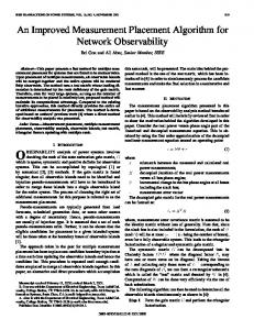
Placement Algorithm for FPGA Circuits ZOLTAN BARUCH, OCTAVIAN CREŢ, KALMAN PUSZTAI Computer Science Department, Technical University of Cluj-Napoca, 26, Bariţiu St., 3400 Cluj-Napoca, Romania {Zoltan.Baruch, Octavian.Cret, Kalman.Pusztai}@cs.utcluj.ro Abstract. Field-Programmable Gate Arrays (FPGAs) are flexible and reusable circuits that can be easily reconfigured by the designer. One of the steps involved in the logic design with FPGA circuits is placement. In this step, the logic functions are assigned to specific cells of the circuit. In this paper we present a placement algorithm for FPGA circuits. In traditional min-cut based placement algorithms, the only metric in the cost function is the cut size. The proposed algorithm not only reduces the cut size and balances the size of the two portions, but also evenly distributes the connections among them. We also propose another sequence of slicing lines which reduces the maximum cut size and the total wirelength of the circuit.
1.
Introduction
Field-Programmable Gate Arrays (FPGAs) are flexible and reusable circuits that can be easily reconfigured by the designer. These circuits represent one of today’s most popular digital logic implementation options. An important component of the FPGA-based design is the computer-aided design (CAD) software necessary to efficiently use the circuits. A typical FPGA design process consists of logic synthesis, technology mapping, placement, and routing. After the logic synthesis phase, the logic specification is divided in the technology mapping phase into logic functions that are directly implemented in the FPGA circuit. In the placement phase, these logic functions are assigned to specific cells of the circuit. Finally, in the routing phase, the logic signals are connected by programmable switches. In this paper, we focus on the placement problem. The placement problem, with the objective to minimize the total wirelength, is NP-complete [1]. Even the simplest case of the problem, i.e., one-dimensional placement, is hard to solve. For real circuits, the solution space is too large to permit enumerative techniques. Therefore, heuristic algorithms are used, which require relatively short execution times (a polynomial function of the number of cells), and can find good solutions to the placement problem, not necessarily the best solutions. Exact algorithms, using techniques like dynamic programming, are computationally expensive. A number of heuristic techniques have been developed for solving the placement problem. A widely used technique for hard combinatorial optimization problems, including placement, is simulated annealing (SA), introduced by Kirkpatrick, Gelatt and Vecchi [2]. A logarithmic temperature scheduling for the SA is proved to ensure global optimum solution. This 1
requires a very slow cooling schedule, which can make SA prohibitively slow. Therefore, an efficient algorithm for the placement problem is desirable. A placement is acceptable if 100% routing can be achieved within a given area. This is not an easy task for FPGA architectures with very limited routing resources, like the Atmel 6000 circuits [3]. A good placement will not only put connected blocks together, but will also ensure that logic elements are not placed too closely in order to ensure the routability of the circuit. Our first contribution is an algorithm which not only reduces the cut size and balances the size of the two portions, but also evenly distributes the connections among them. Our second contribution is another sequence of slicing lines which is more adequate for FPGA circuits than the traditional methods. This sequence reduces the maximum cut size and the total wirelength of the circuit. The rest of this paper is organized as follows. In the next section, we define the placement problem. In Section 3, we briefly describe some related work. In Section 4, we describe the placement algorithm for the FPGA circuits. Experimental results are presented in Section 5. Finally, conclusions are made in Section 6.
2.
The Placement Problem
Given a collection of cells or modules with ports on the boundaries and a collection of nets (which are sets of ports that are to be connected together), the process of placement consists of finding suitable physical locations for each cell on the entire layout. The locations are suitable if they minimize given objective functions, subject to certain constraints imposed by the designer, the implementation process, or layout style. The cells may be standard-cells, macro-cells, FPGA logic blocks, etc. More formally, the placement problem can be defined as follows. Given a set of m modules, M = {M1, M2, …, Mm}, a set of n nets N = {N1, N2, …, Nn}, and a set of p primary input pins and primary output pins R = {R1, R2, …, Rp}, we associate with each module Mi ∈ M a set of nets N Mi , where N Mi ⊆ N. Similarly, we associate with each net Ni ∈ N a set of modules M Ni , where M Ni = {Mj | Ni ∈ N M j }. We are also given a set of locations L = {L1, L2, …, Lk}, where k ≥ n. The placement problem is to assign each Mi ∈ M to a unique location Lj such that some objective function is optimized. Usually each module is considered to be a point, and if Mi is assigned to location Lj then its position is defined by the coordinate values (xj, yj). Sometimes a subset of the modules in M are fixed, i.e., pre-assigned to locations, and only the remaining modules can be assigned to the remaining unassigned locations. Depending on the technology used, different physical placement constraints exist. For gate-array technology, all modules have the same shape and size and are to be placed into predetermined locations on the placement area. For macro-cell technology, modules have different shapes and sizes, and the dimensions wi × hi of Mi for all the modules are given in the circuit specification. The placement area has dimensions W × H and is given in the circuit specification. For performance driven placement, timing specifications are also given. Timing specifications of a circuit include signal arrival times at the primary inputs, the required signal arrival times at the primary outputs, internal delay di of a module Mi, and the maximum allowable signal skew Ci at module Mi for all the modules.
2
3.
Related Work
Algorithms have been developed specifically for the placement of logic in FPGA circuits. Ebeling et al. [4] described automatic mapping tools for the Triptych FPGA architecture. These tools include a placement algorithm based on a simulated annealing approach. Beetem [5] introduced a penalty-driven iterative improvement algorithm for simultaneous placement and routing of FPGAs. Nag and Roy [6] presented an incremental placement algorithm for row-based FPGAs which analyzes post-layout timing and routability information to obtain better placements. Togawa et al. proposed a method for the simultaneous place and route of symmetrical FPGAs based on hierarchical bi-partitioning. Gao [7] developed net-based and path-based performance driven placement algorithms for gate-arrays, macro-cells and Xilinx FPGAs, in order to minimize the signal arrival times at the primary output pins and the signal skews at the inputs of the modules. In the net-based placement algorithm, timing delay requirements are first translated into physical design constraints, such as net constraints. The placement algorithm then generates a placement under the guidance of the net constraints. In the path-based placement algorithm, path delays are considered explicitly during the placement process. This algorithm tries to minimize the total wire length and the latest arrival times at the primary output pins.
4.
Placement Algorithm for FPGA Circuits
A placement algorithm for FPGA circuits must not only minimize the total wirelength by grouping the interconnected cells, but must also ensure the routability of the circuit. We describe a min-cut bi-partitioning based placement algorithm which tries to ensure the routability by evenly distributing the connections among the two portions. We also propose a new sequence of applying slicing lines which is more adequate for FPGA circuits than the traditional sequence. The only metric in the cost function in traditional partitioning algorithms, applied for the placement of FPGA circuits, is the cut size. However, the cut size alone is not a good metric for architectures with limited routing resources, such as FPGA circuits. Since the algorithm tries to place connected blocks close together, it is likely to generate a placement with congested areas, where a feasible routing is difficult to find. In other words, it is possible to obtain a partition with a small cut size, with one portion being heavily connected and the other being very sparse. For FPGA applications, min-cut based placement algorithms must be modified to take into account not only the sizes of the two portions, the size of the network crossing the cut-line, but also the distribution of interconnections within the two portions. We consider that multiple terminal nets are represented by a hyper-graph model. In general, to connect k terminals, max {k-1, 0} connecting paths are needed. We define the unbalancing number of a net to be the number of connecting paths needed to connect all the terminals in the left portion minus the number of connecting paths needed in the right portion. The unbalancing number of a bi-partition is defined to be the sum of the unbalancing numbers of all nets. The absolute value of the unbalancing number of a bi-partition counts the difference between the number of connecting paths needed in the left portion and the right portion [8]. Given an initial bi-partition, we can compute its unbalancing number in O(|T|) time by examining all the nets, where T is the set of all terminals. We assume that there are more interconnecting paths in the left portion than in the right portion, that is, the unbalancing number of this bi-partition is positive. If a node v is moved from the left portion to the right por-
3
tion, we can compute f(v, e), the amount by which the unbalancing number of the net e decreases, by examining the set of all neighbors of v, N(v). The following cost function is used to incorporate the effect of congestion distribution in a given partition: Cut_size + WEIGHT × Unbalancing number where WEIGHT is a constant. If WEIGHT is set to zero, then the algorithm is the same as the conventional min-cut partitioning algorithm. By setting the value of WEIGHT appropriately, we can control the importance of balancing the congestion. In conventional min-cut based placement, the layout region is bi-partitioned using slicing lines in a top-down manner, in accordance with the recursive application of the min-cut bi-partitioning. The sequence in which slicing lines are applied plays an important role. The conventional hierarchical min-cut placement always chooses the cut-line at the center of the current region. If we order the slicing lines to be applied in this sequence, Fig. 1 (a)-(d) shows the sequence of slicing lines to be applied, where slicing lines currently applied are shown as dashed lines and slicing lines applied earlier are shown as solid lines.
Fig. 1. Choosing the slicing line at the center of the current region.
Assume that the current slicing line l, shown as the dashed line in Fig. 2, is immediately next to the center slicing line. Slicing line l will cut four regions and their corresponding sub-networks into halves. In each step of the min-cut bi-partitioning, we can swap a pair of nodes such that one is in A and the other is in E, one is in B and the other is in F, and so on. However, in order to take into account the result of the bi-partitioning for the slicing lines applied earlier, any swapping of nodes that crosses the slicing line applied earlier is not allowed.
Fig. 2. An example in the traditional min-cut placement.
The number of nodes in a region is proportional to the area of that region. Since the slicing line l is close to the center slicing line, the four regions cut by l are small. Therefore, the number of nodes that are placed in regions A-H are small. Consequently, the number of possible pairs that we can choose from for a move in this bi-partitioning process is limited. 4
This usually results in a relatively large cut-size for the slicing lines close to the center due to a small number of possible moves [8]. Based on this observation, we propose another sequence of slicing lines in which they are applied to reduce the congestion near the center. The horizontal slicing lines and vertical slicing lines are applied alternatively as before. However, for the slicing lines of the same orientation, the slicing lines that are closer to the center are applied earlier, as shown in Fig. 3.
Fig. 3. Proposed sequence to apply slicing lines.
5.
Experimental Results
The placement algorithm was implemented in the C language. The experiments were performed on an IBM PC computer with a 200 MHz Pentium-MMX processor, under the Windows NT Version 4.0 operating system. The circuits used are from the MCNC (Microelectronics Center of North Carolina) benchmark suite. The experiments were conducted as follows. The standard circuits were converted from the EDIF format (Electronic Design Interchange Format) to the netlist format used by the technology mapping program. The circuits were then technology mapped for the Atmel 6002 FPGA circuit. The placement process was applied to the netlists obtained after the technology mapping. Table 1. The sum of the cut sizes for the proposed algorithm and the traditional algorithm. Circuit b1 c17 cm138a con1 decod majority tcon x2
Proposed Algorithm 13 8 23 17 44 11 45 38
W=0 Traditional Algorithm 19 10 38 30 69 17 60 51
Reduction 31.5 % 20.0 % 39.4 % 43.3 % 36.2 % 35.2 % 25.0 % 25.4 %
Proposed Algorithm 15 8 28 17 51 11 41 42
W=1 Traditional Algorithm 17 10 38 28 59 15 51 46
Reduction 11.7 % 20.0 % 26.3 % 39.2 % 13.5 % 26.6 % 19.6 % 8.6 %
In Table 1 we compared the sum of the cut sizes for all the slicing lines applied, for the proposed algorithm and the traditional algorithm. The comparison was made for two cases. The first case is without balancing the number of connections in the two portions (WEIGHT = 0), indicated in the table by W = 0, and the second case is with balancing the connections (WEIGHT = 1), indicated in the table by W = 1. The reduction of the total cut sizes ranges between 20% and 43.3% when W = 0, with an average of 32%, and ranges between 8.6% and 39.2% when W = 1, with an average reduction of 20.6% in this case. 5
In Table 2 we compared the maximum cut sizes for all the slicing lines applied, for the proposed algorithm and the traditional algorithm. The reduction obtained by the proposed algorithm is up to 30% when W = 0, with an average reduction of 17.7%, and up to 35.7% when W = 1, with an average reduction of 22.8%. Table 2. The maximum cut sizes for the proposed algorithm and the traditional algorithm. Circuit b1 c17 cm138a con1 decod majority tcon x2
6.
Proposed Algorithm 7 4 9 9 10 7 10 12
W=0 Traditional Algorithm 9 4 12 12 12 10 11 14
Reduction 22.2 % 0.0 % 25.0 % 25.0 % 16.6 % 30.0 % 9.0 % 14.2 %
Proposed Algorithm 8 4 14 8 15 9 14 12
W=1 Traditional Algorithm 11 6 16 10 17 14 17 16
Reduction 27.2 % 33.3 % 12.5 % 20.0 % 11.7 % 35.7 % 17.4 % 25.0 %
Conclusions
In this paper we presented a min-cut bi-partitioning based placement algorithm for FPGA circuits. The algorithm was implemented for the Atmel 6002 FPGA circuits. The proposed algorithm not only reduces the cut size and balances the size of the two portions, but also evenly distributes the connections among them, in order to ensure the routability of the circuit. We also proposed another sequence of slicing lines which is more adequate for FPGA circuits than the traditional sequence. The proposed sequence reduces the maximum cut size and the total wirelength of the circuit. The experimental results show the efficiency of the algorithm.
7.
References [1] S.M. Sait and H. Youssef, “VLSI Physical Design Automation”, McGraw-Hill Book Company, 1995 [2] S. Kirkpatrick, C.D. Gelatt and M.P. Vecchi, “Optimization by Simulated Annealing”, Science, No. 220, pp. 671-680, May 1983 [3] Atmel Corp., “Configurable Logic. PLD, FPGA, Gate Array Data Book”, San Jose, 1995 [4] C. Ebeling, L. McMurchie, S.A. Hauck and S. Burns, “Placement and Routing Tools for the Triptych FPGA”, IEEE Transactions on Very Large Scale Integration (VLSI) Systems, Vol. 3, No. 4, pp. 473-482, December 1995 [5] J. Beetem, “Simultaneous Placement and Routing of the LABYRINTH Reconfigurable Logic Array”, The International Workshop of Field-Programmable Logic and Applications, Oxford, U.K., pp. 232-243, 1991 [6] S. Nag and K. Roy, “Iterative Wireability and Performance Improvement for FPGAs”, Proceedings of the 30th Design Automation Conference, pp. 321-325, 1993 [7] T. Gao, “Performance Driven Placement and Routing Algorithms”, Ph.D. Thesis, University of Illinois at Urbana-Champaign, 1994 [8] Z. Baruch, “Contributions to the Computer Aided Design of Digital Systems”, Ph.D. Thesis, Computer Science Department, Technical University of Cluj-Napoca, 1998
6