A Complete Electronic Network Interface Architecture for Global Contention-Free Communication over Emerging Optical Networks-on-Chip Marta Ortín-Obón§ , Luca Ramini† , Herve Tatenguem Fankem† , Víctor Viñals§ , Davide Bertozzi† §
†
gaz-DIIS-i3A, University of Zaragoza, Spain. {ortin.marta, victor}@unizar.es ENDIF, University of Ferrara, Italy. {luca.ramini, herve.tatenguemfankem, davide.bertozzi}@unife.it
ing path. Despite their limited scalability, these networks are attractive for specific application domains, where performance predictability and ultra-low latency communications are a must (e.g. data center applications [11]). WRONoCs can be conceptualized as non-blocking full crossbars. Therefore, all the complexity of the control architecture is located at the boundary of the interconnect fabric. To our knowledge, no complete NI architecture has been reported so far in the open literature, with the exception of NIs for space-routed ONoCs. However, these are conceptually simpler due to the intuitive conversion of electrical bit parallelism into optical wavelength parallelism [9]. In contrast, WRONoCs rely on serialization or on a limited bit parallelism, which questions the achievement of performance goals. Even neglecting this difference, the NI design for an optical medium is a non-trivial task due to the interdependent issues that come to the forefront: end-to-end flow control, buffer sizing, clock re-synchronization, and serialization ratio. This paper takes on the challenge of designing and characterizing the complete NI architecture for emerging WRONoCs, in an attempt to validate whether (and to what extent) the projected benefits of optical NoCs over their electrical counterpart are still preserved with the NI in the picture. The distinctive feature of this work is the completeness of the architecture, including both initiator and target side. Especially, the digital architecture to enable optical NoC operation has been designed out of state-of-the-art basic building blocks (e.g., mesochronous synchronizers and dual-clock FIFOs), thus reflecting realistic quality metrics. The system-level requirements of a target multi-core processor with cache-coherent memory architecture have a large impact on the interface footprint. Finally, for the optical and opto-electronic components, we used a consistent set of static and dynamic power values from the same literature source [2, 1]. Our evaluation methodology consists of 2 steps: first, we synthesize and characterize latency, and power for all of the architecture components on a low power industrial 40 nm technology; second, we set up a complete SystemC-based simulation infrastructure (for both the optical and electronic parts) with RTL-equivalent accuracy, thus enabling to capture fine grained performance effects associated with the microarchitecture.
ABSTRACT Although many valuable research works have investigated the properties of optical networks-on-chip (ONoCs), the vast majority of them lack an accurate exploration of the network interface architecture (NI) required to support optical communications on the silicon chip. The complexity of this architecture is especially critical for a specific kind of ONoCs: the wavelength-routed ones. From a logical viewpoint, they can be considered as full nonblocking crossbars, thus the control complexity is implemented at the NIs. To our knowledge, this paper proposes the first complete NI architecture for wavelength-routed optical NoCs, by coping with the intricacy of networking issues such as flow control, buffering strategy, deadlock avoidance, serialization, and above all, with their codesign in a complete architecture.
1.
INTRODUCTION
The current research frontier for on-chip interconnection networks consists of assessing the feasibility of the optical interconnect technology, by exploiting the recent remarkable advances on silicon photonics [7]. The literature on this topic is becoming quite rich, mainly projecting superior bandwidth, latency and energy with respect to electrical wires beyond a critical length [12]. This benefits are extended to on-chip communication architectures, either as standalone optical networks (ONoCs) [13], or as hybrid interconnect fabrics [4]. Nonetheless, projected quality metrics are overly optimistic for a number of reasons extensively discussed in [1], including optimistic technology assumptions, use of logical topology designs instead of physical ones, and overlooking static power. A big approximation of many projected results is the lack of a complete and accurate network interface architecture for driving on-chip optical communication, which may account for a large fraction of the overall network complexity. This is especially true for a particular category of ONoCs: the Wavelength-Routed ones (WRONoCs). These networks deliver contention-free global connectivity without need for arbitration or packet routing by replicating the amount of wavelengths used, and by associating each wavelength with a different and non-conflicting optical routPermission to make digital or hard copies of all or part of this work for personal or classroom use is granted without fee provided that copies are not made or distributed for profit or commercial advantage and that copies bear this notice and the full citation on the first page. Copyrights for components of this work owned by others than the author(s) must be honored. Abstracting with credit is permitted. To copy otherwise, or republish, to post on servers or to redistribute to lists, requires prior specific permission and/or a fee. Request permissions from
[email protected]. GLSVLSI’14, May 21–23, 2014, Houston, Texas, USA. Copyright is held by the owner/author(s). Publication rights licensed to ACM. ACM 978-1-4503-2816-6/14/05 ...$15.00. http://dx.doi.org/10.1145/2591513.2591536 .
2.
RELATED WORK
Early ONoC evaluation studies rely on coarse, higherlevel models and/or unrealistic traffic patterns [19, 23, 10, 18], while more recent ones come up with complete end-toend evaluations using real application workloads [14] and/or more accurate optical network models [5]. Looking in re-
267
λ1
I1
λ2
λ4
λ3 λ3
NI
T1
REQUEST RESPONSE
T2
MEMORY CONTROLLER WAIT-FOR
λ4
T3
Figure 2: Dependence between a request and reponse at the NI.
λ1
I2
λ2
T4
NoC by allocating a different buffer for each kind of message in the NI. This has direct implications on the buffering architecture of our target NI (that is, on the number of virtual channels), depending on the communication protocols the WRONoC needs to support. As a consequence, we make an assumption on a target system architecture. Without lack of generality, we focus on a homogeneous chip multiprocessor with 16 cores, similar to the Tilera architecture [22]. Each core has a private L1 cache and a bank of the shared distributed L2 cache, both connected to a common NI through a crossbar. The system has directory-based coherence managed with a MESI protocol. By analysing the dependency chains of the protocol and deadlock-free buffer sharing opportunities, we came up with a requirement of 3 VCs for deadlock avoidance. Proof is omitted for lack of space.
Figure 1: Wavelength-selective routing trospect, early results have been only partially confirmed, nonetheless showing the potential of ONoCs for on-chip communication. The refinement of comparative analysis frameworks is far from stabilizing. In fact, other missing aspects are progressively coming to the forefront as the ONoC research concept strives to become an industry-relevant technology. So far, the NI architecture has been overlooked in most evaluation frameworks, or in the best case, only considered in the early stage of design. Some pioneer works account for the NI in their network analysis for wavelength-routed optical networks [17, 1, 3], or space-routed ONoCs [9]. In every case, they suffer from one of the following weaknesses: first, they model NI components only at behavioural level [17], or they target only the more abstract level of formalization of interface specification [3]; second, they consider only the signal driving section of the ONoC, basically up to the (de)serializers. This way, higher-level network architecture design issues such as flow control, synchronization, or buffering architecture are overlooked. The distinctive features of our approach are: architecture completeness, comparison with electrical interface counterparts, physical synthesis of digital components, RTLequivalent SystemC modeling for microarchitectural performance characterization, and analysis of the impact of NI quality metrics on global network ones.
3.
5.
BACKGROUND ON WRONOCS
Wavelength-routed optical NoCs rely on the principle of wavelength-selective routing. As it is conceptually showed in Figure 1, every initiator can communicate with every target at the same time by using different wavelengths. The topology connectivity pattern is chosen to ensure that wavelengths will never interfere with each other on the network optical paths. This way, all initiators can communicate with the same target by using different wavelengths. WRONoCs support contention-free all-to-all communication with a modulation speed of 10 Gbps/wavelength. Our NI can work with any WRONoC topology. Without lack of generality, we model a wavelength-routed ring inspired by [15] implemented on an optical layer vertically stacked on top of the baseline electronic layer.
4.
NI ARCHITECTURE
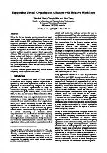
This section presents, to the best of our knowledge, the first complete network interface architecture for wavelengthrouted optical networks, as depicted in Figure 3. As a consequence, the objective is not to present the best possible design point, but rather to start considering the basic components, and deriving guidelines about which ones deserve the most intensive optimization effort. Clearly, ONoCs move most of their control logic to the NIs, which should therefore not be oversimplified with abstract models. To avoid message-dependent deadlock, every NI needs separate buffering resources (virtual channels, VCs) for each one of the three message classes of the MESI protocol. This should be combined with the requirements of wavelength routing: each initiator needs an output for each possible target, and each target needs an input for each possible initiator. As a result, each target comes with 3 FIFOs for each potential initiator. In the transmission side, the same 3 FIFOs are shared for all destinations and flits are sent to different paths afterwards (all the logic components after the 1x15 demultiplexers are replicated for each destination). All the FIFOs at both the transmission and the reception side must be dual-clock FIFOs (DC FIFOs) to move data between the processor frequency domain (we assume 1.2GHz) and the one used inside the NI. As hereafter explained, the latter depends on the bit parallelism. We used the DC FIFO architecture presented in [21]. To size the DC FIFOs, we considered the size of the packets that would use each of the VCs: control packets need 2 flits, while data packets need 21 flits assuming flits are always 32 bits long. The FIFO depth will be assessed in the experimental results. The minimum size for the DC FIFO to achieve perfect throughput is 5 slots [21], so all the VCs in the transmission side have been sized this way. For the reception side, we sized the data VC based on the round-trip latency in order to allow uninterrupted communications, ending up with 15-slot DC FIFOs. However, for the control VCs we decided to keep small 5-slot DC FIFOs because they can already fit two complete packets and we do not expect to send many back-to-back control packets with the target cache-coherence protocol.
TARGET ARCHITECTURE
During the design of the NI, we consider a high-impact system requirement: message-dependent deadlock avoidance. Message-dependent deadlock arises from the interactions and dependencies created at network endpoints between different message types (as depicted in Figure 2) [6, 8]. In a complete system, the combination of these effects may lead to cyclic dependencies and block resources at both network endpoints and inside the network indefinitely. When we apply these considerations to WRONoCs, the problem gets simplified by the fact that there is no buffering inside the network, which means messages don’t stop along the path, and, therefore, can’t get blocked. However, we must break the dependency cycles at the boundaries of the
268
DC_FIFO 5slots
dest DECOD
VC
MUX 4x1
dest DECOD
DEMUX 1x15
DC_FIFO 5slots
credit flit
BRUTE FORCE SYNC
Driver
11 BITSER
Driver
11 BITSER
Driver
DC_FIFO 5slots
H1 H1
DC_FIFO 5slots DC_FIFO 15slots
H15 H15 H15
1.2 GHz (0.83 ns/cycle)
λ11 λ12 λ13
TSV
ELECTRONIC TSV CLOCK SOURCE
λ1clk OPTICAL NOC
MESOCHRONOUS SYNCHRONIZER CLOCK DIVIDER
DEMUX 1x4
MUX [15x3]x1
H1
TSV TSV
credits
ARBITER
ultra-low complexity design point. Each 32-bit switch includes 3 VCs to avoid message-dependent deadlock, with 5 slots each. It takes one cycle to traverse the switch and one cycle to traverse each link. When it comes to the network interface, it consists of two parts [14]. The first one is a packetizer, which acts as protocol converter from the IP core to the network. This block is also required for the ONoC, so it is not considered in this comparison framework The second one is the buffering stage. In order to preserve the generality of the design and support cores with different operating frequencies that access an ENoC with fixed common frequency, dual-clock FIFOs have been included at the electronic network interfaces, similar to the ONoC NI design. However, in this case all DC FIFOs have 5 slots at both initiator and target side, because round-trip latency does not require larger buffers for maximum throughput operation.
RING MODULATOR
11 BITSER
ARBITER
CREDIT COUNTER
OPTICAL SIDE
ELECTRONIC TRANSMISSION SIDE
DEMUX 1x15
dest DECOD
DEMUX 1x15
DEMUX 1x3
VC DECOD
DC_FIFO 5slots
COMP
TIA
11 BITDESER
COMP
TIA
11 BITDESER
COMP
TIA
11 BITDESER
COMP
TIA
TSV TSV TSV TSV
PD
λ1clk
PD
λ11
PD PD
λ12 λ13
ELECTRONIC RECEPTION SIDE 0.9 GHz (1.1 ns/cycle)
10 GHz (0.1 ns/cycle)
7.
6.
EVALUATION
This section characterises the most important networkquality metrics for the electro-optical NI. Results for an ENoC configured with typical parameters from [20] are also included. This aims to set the bases for a future comprehensive crossbenchmarking study, which is out of the scope of this paper.
Figure 3: Optical Network Interface Architecture for 3-bit parallelism After flits are sent to the appropriate path depending on their destination, they must be translated into a 10 GHz bit stream in order to be transmited through the optical NoC. This serialization process is parallelized to some extent to increase bandwidth and reduce latency. 3-bit parallelism means that 3 serializers of 11 bits each work in parallel to serialize the 32 bits of a flit, resulting on a bandwidth of 30 Gbps. The bit-parallelism determines the frequency inside the optical NI: 1.1 ns (0.1*number of bits) are needed to serialize a flit with 3-bit parallelism, but only 0.8 ns are needed with 4-bit parallelism. In turn, this also impacts the size of the reception DC FIFO based on round-trip latency, which increases from 15 to 17 slots when moving from 3 to 4-bit parallelism. Another key issue to be considered in NIs is the resynchronization of received optical pulses with the clock signal of the electronic receiver. In this paper we assume sourcesynchronous communication, which implies that each pointto-point communication requires a strobe signal to be transmitted along with the data on a separate wavelength. With current technology, this seems to be the most realistic solution, even considering the promising research effort that is currently being devoted to transmitting clock signals across an optical medium [16]. The received source-synchronous clock at the reception side of the NI is then used to drive the de-serializers and, after a clock divider, the front-end of the DC FIFOs. We assume that a form of clock gating is implemented, so when no data is transmitted, the optical clock signal is gated. Another typically overlooked issue is the backpressure mechanism. We opt for credit-based flow control because credit tokens can reuse the existing communication paths. Besides, the low dynamic power of ONoCs can easily tolerate the signalling overhead of this flow control strategy. Credits are generated at the reception side of the NI when a flit leaves the DC FIFO (at the processor frequency) and forwarded to the transmission side so that they can be sent back to the source (at the NI frequency). To synchronize between different frequency domains, we used brute force and mesochronous synchronizers.
7.1
Methodology
To obtain accurate latency results, we implemented detailed RTL models of the optical and electronic network interfaces and NoCs using SystemC. We instantiated a 4x4 2D mesh for the electronic NoC, and a similar system connected by the optical ring. The network-wide focus, well beyond the NI, aims at relating NI quality metrics to network ones. Delay values for the optical ring have been backannotated from physical-layer analysis, and have been differentiated on a per-path basis. For power modeling, every electronic component has been synthesized, placed and routed using a low power 40 nm industrial technology library. Power metrics have been calculated by backannotating the switching activity of block internal nets, and then importing waveforms in the PrimeTime tool. We have applied clock gating to achieve realistic static power values. Energy-per-bit has been computed by assuming 50% switching activity. Table 1 sums up the static power and energy-per-bit for all the electronic and optical devices. For the fast developing optical technology, we consider a coherent set of both conservative and aggresive parameters [2, 1].
7.2
NI Latency Breakdown
Figure 4 presents the latency breakdown for the NI components and the ONoC, obtained from our accurate RTLequivalent simulations. We clearly see that the latency of the network is negligible, but it requires support from a time consuming NI. Inside the NI, the DC FIFOs are the components with the largest latency.
7.3
Transaction Latency
We simulate the most common traffic patterns generated by a MESI coherence protocol in our RTL models without any contention. The increased accuracy of our analysis stems from the fact that our packet injectors and ejectors model actual transactions of the protocol, as well as their interdependencies. Table 2 describes the analysed compound transactions and Figure 5 presents the zero-load latency results. The messages included in these patterns amount to
BASELINE ELECTRONIC NOC
The baseline electronic switch architecture is the consolidated ×pipesLite architecture [20], which represents an
269
Table 1: Static Power and Dynamic Energy of Electronic and Optical Devices. HARDWARE count per NI
COMPONENTS DC FIFO 5slots (TX) DC FIFO 5slots (RX) DC FIFO 15-17 slots DEMUX1x3 DEMUX1x15 DEMUX1x4 MUX4x1 + ARB MUX45x1 + ARB SERIALIZER DESERIALIZER MESO-SYNCHRONIZER COUNTER 2bits BRUTE FORCE SYNC CLOCK DIVIDER TSV TRANSMITTER aggressive TRANSMITTER conservative RECEIVER aggressive RECEIVER conservative THERMAL TUNING/RING 20K LASER POWER aggressive LASER POWER conservative E-SWITCH (3VCs) DC FIFO ctrl: 3.31ns data: 3.81ns
Comb. logic 1.1ns
DC FIFO ctrl: 2.91ns data: 2.68ns
Serializer 0.1ns
De-serializer 1.1ns
3 30 15 1 3 15 15 1 45 45 45 45 15 15 120 60 60 60 60 180 / / /
3-bit parallelism STATIC DYNAMIC POWER ENERGY (mWatts) (fJ/bit) 0.12 10.65 0.12 8.54 0.12 26.50 0.000725 0.92 0.0021 25.21 0.00056 6.72 0.08 0.36 0.9 5.09 0.0475 9.41 0.0289 7.74 0.041 8.00 0.01482 1.014 0.004234 1.4 0.01172 0.6 / 2.50 0.025 20 0.100 50 0.050 10 0.150 25 0.020 / 0.0421 / 0.308 / 17.9 193
ONoC min: 0.023ns max: 0.320ns
id
Event
P1a
L1 miss
P1b/c
Total latency: ctrl flit = 9.04ns; data flit = 9.31ns
Figure 4: Latency breakdown of the optical NI with 3-bit parallelism and the optical ring. an average 99.9% of the total network traffic, as we observed from full-system simulations of realistic parallel benchmarks from PARSEC and SPLASH2 and multiprogrammed workloads built with SPEC applications (we only exclude communication with the memory controllers). Therefore, they are a very good indicator of the network latency improvements we can expect from the optical network, including its (non-negligible) network interface overhead. We observe that in all the patterns except the last one, the ONoCs either beat or obtain equal results to the ENoC with all path lenghts. As opposed to the ENoC, most of the latency of the ONoC is spent in the NI, which is needed to support the low latency optical communication. The tendency changes in pattern 5 because the replacement packet is using a VC designed for control to transmit data, and the smaller FIFO cannot store enough flits to support the round-trip latency. However, this messages are only 7.4% of the total network traffic.
L1 write miss, 1/2 sharers
P2a
L1 needs upgrade to write
P2b/c
L1 needs upgrade to write, 1/2 sharers
P3
P4
P5
L1 write miss, another owner L1 read miss, another owner L1 replacement ENoC min ENoC max
100
Sequence of messages 1. Request from L1 to L2 2. Data reply from L2 to L1 3. ACK from L1 to L2 1. Request from L1 to L2 2. L2 sends data reply and invalidates 1/2 sharers 3. Sharers sends ACK to L1 req. 4. ACK from L1 to L2 1. Request from L1 to L2 2. ACK reply from L2 to L1 3. ACK from L1 to L2 1. Request from L1 to L2 2. ACK reply from L2 to L1 and invalidates 1/2 sharers 3. Sharers send ACK to L1 req. 4. ACK from L1 to L2 1. Request from L1 to L2 2. L2 forwards request to owner 3. Owner sends data to L1 4. ACK from L1 to L2 1. Request from L1 to L2 2. L2 forwards request to owner 3. Owner sends data to L1 and L2 4. ACK from L1 to L2 1. Writeback from L1 to L2 2. ACK from L2 to L1 ENoC avg 3−bit ONoC
4−bit ONoC
90
Throughput
Latency (ns)
7.4
3 30 15 1 3 15 15 1 60 60 45 45 15 15 150 75 75 75 75 225 / / /
Table 2: Messages generated by the coherence protocol.
E/O conv. 0.1ns
O/E conv. 0.1ns
count per NI
4-bit parallelism STATIC DYNAMIC POWER ENERGY (mWatts) (fJ/bit) 0.12 12.72 0.12 10.2 0.12 31.65 0.000725 0.92 0.0021 25.21 0.00056 6.72 0.11 0.49 0.9 5.09 0.0417 2.63 0.0281 6.12 0.0565 11.1 0.01482 1.014 0.00503 1.66 0.0139 0.714 / 2.50 0.025 20 0.100 50 0.050 10 0.150 25 0.020 / 0.0525 / 0.385 / 17.9 193
We test the behaviour of the electronic and optical networks under contention. To do that, we focus only on requests and data replies. We leave the ACKs out because they are not in the critical path of the communications. We monitor transactions between an L1 and an L2 located in different nodes, and gradually insert congestion by sending requests from the other nodes to the same L2. Figure 6 presents the results for the ENoC and the 3, 4 and
80 70 60 50 40 30 P1a
P1b
P1c
P2a
P2b
P2c
P3
P4
P5
Figure 5: Latency of the most common communication patterns. For the ENoC, we include minimum, maximum, and average paths.
270
ENoC
3−bit ONoC
4−bit ONoC
6−bit ONoC
Table 3: Buffer sizes explored for the 3 VCs at each side of the NI. Note that the actual capacity of the DC FIFOs is one flit less than the number of slots. id Transmission side Reception side A 3, 3, 3 3, 3, 3 B 3, 3, 5 3, 3, 5 C 5, 5, 5 5, 5, 5 D 5, 5, 5 5, 5, 15 E 5, 5, 22 5, 5, 15 F 10, 10, 44 10, 10, 44
25 20 15 10 5 0 0
1
2
3
4 5 6 Number of Interferers
7
8
14
10000 Transaction Latency (ns)
Completed Transactions /1000ns
30
Figure 6: Number of completed transactions per 1K ns between two nodes as the number of interferers increases. 6-bit parallelism ONoCs. Without contention, more transactions get completed in the optical NoC because their latency is lower. As we keep increasing the number of interferers, the throughput for the 3-bit parallelism ONoC drops much faster than for the ENoC. This is because the former can eject a maximum of 30 Gbps, while the latter transmits flits at 38.4 Gbps. For this reason, replies need to wait much longer until they can be transmitted. However, when considering the 4-bit parallelism ONoC, which has a bandwidth of 40 Gbps, we see results comparable and even superior to those of the ENoC. At 6-bit parallelism, the increased bandwidth (60 Gbps) only gives the ONoC a slight advantage, which is not enough to justify the increase in static power (as later documented).
7.5
100
10 1 4 15 Number of Simultaneous Requestors
Figure 7: Transaction latency with varying buffer sizes. 10.6% and 11.8% for the aggressive technology with 3 and 4-bit parallelism, respectively. It is worth highlighting that most of the static power of the electronic components in the NI comes from the DC FIFOs. Also, the savings in execution time of the ONoC vs the ENoC may compensate the higher static power and result in overall energy reductions. This is especially true when we consider the power of the system as a whole [14]. For energy-per-bit we included minimum, maximum and average path lengths for the ENoC and specific values for control and data packets for the ONoC (which change due to the different size of the reception DC FIFOs). We clearly see that the ONoC has significantly lower energy-per-bit than the ENoC, which confirms the trend from previous literature. Apart from that, we still see how the main contributor for the ENoC energy is the NoC, while the NI carries all the complexity for the ONoC.
Buffer Size Exploration
In this section we analyse the effect of modifying the buffering of the optical network interface. We fix the bit parallelism at 3 and explore all the buffer size combinations detailed in table 3. Figure 7 shows how buffer size in the NI affects transaction latency, using the same request-reply pattern as in the previous section. In case A, the minimum buffering has a very negative impact on performance, because data packets are stalled waiting for credits from the reception side FIFOs, which can only store 2 flits. This effect is slightly mitigated when we increase the buffer size for this VC to 5 slots in case B. Even though the DC FIFOs can achieve perfect throughput, backpressure is still preventing faster communications. We don’t see any difference by increasing the size of control VCs in case C because the bottleneck is in the data VC. However, in case D, the reception side has been sized based on the round-trip latency and we achieve the maximum possible throughput. The larger buffers in cases E and F do not show any further improvements because the network is already using up all the bandwidth.
7.6
A B C D E F
1000
8.
CONCLUSIONS
This paper presents an accurate design of NIs for WRONoCs, captures the effect on the most important network-quality metrics, and sets the scene for further comparative ONoC analysis. Regarding latency, the ONoC is always faster than its electronic counterpart even considering the NI, thus preserving the primary goal of a WRONoC. The behaviour under contention depends mainly on the available bandwidth of the interconnect technologies under test. For the WRONoC, such bandwidth can be modulated by tuning the bit parallelism, and adjusting buffer size to flow control requirements for maximum throughput operation. Similar tuning knobs do exist for ENoCs, namely flit width and buffer sizes. Therefore, the ultimate question is whether such tuning knobs are energy efficient in comparative terms, which depends on the sensitivity of system performance to such knobs for the application at hand. This is left for future work. When we consider power figures, we notice that, while switches are the main contributors in ENoCs, the NI has the largest share in ONoCs. For static power, this contribution is in the same order of magnitude than that from laser sources with conservative optical technology parameters. However, by further improving the optical technology, the role of the NI becomes dominant, thus making it the main target for future optimizations. Finally, the ONoC pre-
Power and Energy-per-Bit
Figure 8 depicts the static power and (dynamic) energyper-bit for the ENoC vs. the 3 and 4-bit parallelism ONoCs. We do not consider ONoCs with less than 3-bit parallelism because the bandwidth of the optical paths would be too low, or ONoCs with more than 4-bit parallelism, because the static power becomes unacceptable (we can see a clear trend in Figure 8). We present a breakdown of the contributions of the NIs (electronic and optical components) and NoCs. The optical NoC is solely composed of laser power, so it has no impact on dynamic energy. We observe that the electronic switches dominate the static power, accounting for 95.8% of the total. However, this trend is reversed in the ONoC, with a contribution of only
271
Energy per bit (pJ/bit)
Static Power (W)
0.8
0.5
0.8
0.6
0.4
0.2
0.0
1.4
0.6
1.0
optical NoC
0.4
electronic NoC 0.3 NI optical components NI electronic components
0.2 0.1
ENoC
aggr cons 3bit ONoC
aggr cons 4bit ONoC
0.0
min
max avg ENoC
aggr cons aggr cons 3b,ctrl 3b,data
aggr cons aggr cons 4b,ctrl 4b,data
b) Energy per bit
a) Static Power
Figure 8: Static power and Energy-per-Bit of the NIs and the electronic and optical NoCs. serves its superior dynamic power properties over its ENoC counterpart, even in the presence of its NI. This paper shows that the NI architecture should not be overlooked for realistic ONoC assessments, and comes up with new insights not provided by earlier photonic network evaluations. The most important one is that NI optimizations perhaps have higher priority over the relentless search for ultra-low-loss optical devices.
9.
[11]
[12]
ACKNOWLEDGMENTS
[13]
This work was supported by grants TIN2010-21291-C0201 (Spanish Government, European ERDF), IT FIRB Photonica (RBFR08LE6V) project, and HiPEAC-3 NoE (European FP7/ICT 217068).
10.
[14]
REFERENCES
[1] C. Batten, A. Joshi, V. Stojanovic, and K. Asanovic. Designing chip-level nanophotonic interconnection networks. IEEE Journal on Emerging and Selected Topics in Circuits and Systems, pages 137–153, 2012. [2] S. Beamer, C. Sun, Y.-J. Kwon, A. Joshi, C. Batten, V. Stojanovic, and K. Asanovic. Re-architecting DRAM memory systems with monolithically integrated silicon photonics. In ISCA, pages 129–140. ACM, 2010. [3] M. Biere, L. Gheorghe, G. Nicolescu, I. O’Connor, and G. Wainer. Towards the high-level design of optical networks-on-chip. Formalization of opto-electrical interfaces. In Int.Conf. on Electronics, Circuits and Systems., pages 427–430, 2007. [4] J. Chan, G. Hendry, A. Biberman, and K. Bergman. Architectural design exploration of chip-scale photonic interconnection networks using physical-layer analysis. In Optical Fiber Communication (OFC), pages 1–3, 2010. [5] J. Chan, G. Hendry, A. Biberman, and K. Bergman. Architectural exploration of chip-scale photonic interconnection network designs using physical-layer analysis. Journal of Lightwave Technology, pages 1305–1315, 2010. [6] W. Dally and B. Towles. Principles and Practices of Interconnection Networks. Morgan Kaufmann Publishers Inc., San Francisco, CA, USA, 2003. [7] C. G. et al. A cmos-compatible silicon photonic platform for high-speed integrated opto-electronics. Proc. Integrated Photonics: Materials, Devices, and Applications, 2013. [8] A. Hansson, K. Goossens, and A. Radulescu. Avoiding message-dependent deadlock in network-based systems on chip. VLSI Design, 2007. [9] G. Hendry, J. Chan, S. Kamil, L. Oliker, J. Shalf, L. Carloni, and K. Bergman. Silicon nanophotonic network-on-chip using TDM arbitration. In Annual Symp. on High Perf. Interconnects (HOTI), pages 88–95, 2010. [10] A. Joshi, C. Batten, Y.-J. Kwon, S. Beamer, I. Shamim, K. Asanovic, and V. Stojanovic. Silicon-photonic clos
[15]
[16]
[17] [18]
[19]
[20]
[21]
[22]
[23]
272
networks for global on-chip communication. In Int. Symp on Networks-on-Chip, pages 124–133, 2009. R. Kapoor, G. Porter, M. Tewari, G. M. Voelker, and A. Vahdat. Chronos: Predictable low latency for data center applications. In Procs of the ACM Symp. on Cloud Comp., pages 9:1–9:14, 2012. P. Kapur and K. C. Saraswat. Optical interconnects for future high performance integrated circuits. Physica E: Low-dimensional Systems and Nanostructures, pages 620 – 627, 2003. S. Koohi, M. Abdollahi, and S. Hessabi. All-optical wavelength-routed NoC based on a novel hierarchical topology. In Procs of the Int. Symp. on Networks-on-Chip, NOCS ’11, pages 97–104, 2011. G. Kurian, C. Sun, C.-H. Chen, J. Miller, J. Michel, L. Wei, D. Antoniadis, L.-S. Peh, L. Kimerling, V. Stojanovic, and A. Agarwal. Cross-layer energy and performance evaluation of a nanophotonic manycore processor system using real application workloads. In Int. Parallel Distributed Processing Symposium (IPDPS), pages 1117–1130, 2012. S. Le Beux, J. Trajkovic, I. O’Connor, G. Nicolescu, G. Bois, and P. Paulin. Optical ring network-on-chip (ORNoC): Architecture and design methodology. In Design, Automation Test in Europe Conference Exhibition (DATE), pages 1–6, 2011. J. Leu and V. Stojanovic. Injection-locked clock receiver for monolithic optical link in 45nm soi. In Solid State Circuits Conference (A-SSCC), 2011 IEEE Asian, pages 149–152, 2011. I. e. a. O’Connor. Towards reconfigurable optical networks-on-chip. RECO SoC, pages 121–128, 2005. Y. Pan, J. Kim, and G. Memik. Flexishare: Channel sharing for an energy-efficient nanophotonic crossbar. In Int. Symp. on High Performance Computer Architecture, pages 1–12, 2010. Y. Pan, P. Kumar, J. Kim, G. Memik, Y. Zhang, and A. Choudhary. Firefly: Illuminating future network-on-chip with nanophotonics. In Procs. of the Int. Symp. on Computer Architecture, ISCA ’09, pages 429–440, 2009. S. Stergiou, F. Angiolini, S. Carta, L. Raffo, D. Bertozzi, and G. De Micheli. xpipes lite: a synthesis oriented design library for networks on chips. In Design, Automation and Test in Europe, pages 1188–1193 Vol. 2, 2005. A. Strano, D. Ludovici, and D. Bertozzi. A library of dual-clock fifos for cost-effective and flexible mpsoc design. In Int. Conf. on Embedded Computer Systems (SAMOS), pages 20–27, 2010. TileraCorporation. Tile-Gx8016 specification. http://www.tilera.com/sites/default/files/ productbriefs/Tile-Gx-8016-SB011-03.pdf. D. Vantrease, N. Binkert, R. Schreiber, and M. Lipasti. Light speed arbitration and flow control for nanophotonic interconnects. In MICRO-42, pages 304–315, 2009.