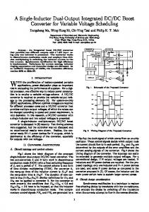
2011 Published by Elsevier Ltd. Selection and/or peer-review under ... With the high speed development of power electronics, switching power supplies are ...
Available online at www.sciencedirect.com Available online at www.sciencedirect.com
Physics Procedia
Physics Procedia 00 (2011) Physics Procedia 24000–000 (2012) 2053 – 2058 www.elsevier.com/locate/procedia
2012 International Conference on Applied Physics and Industrial Engineering
A Composite PWM Control Strategy for Boost Converter Liu Qingfeng, Leng Zhaoxia, Sun Jinkun, Wang Huamin School of Automation and Information Engineering Xi’an University of Technology Xi’an, CHINA
Abstract In order to improve the control performance of boost converter with large signal disturbance, a composite PWM control strategy for boost converter operating in continuous condition mode (CCM) was proposed in this paper. The parasitical loss of Boost converter was analyzed and a loss compensation strategy was adopted to design feed-forward tracker for converter. The composite PWM controller consisted of the tracker and PID controller. Simulation and experiment results validated the validity of the control strategy presented in this paper. © 2011 Published by Elsevier B.V. Selection and/or peer-review under responsibility of ICAPIE Organization Committee.
© 2011 Published by Elsevier Ltd. Selection and/or peer-review under responsibility of [name organizer]
Open access under CC BY-NC-ND license.
Keywords:boost converter; continuous condition mode; loss; feed-forward tracker; composite control
1. Introduction With the high speed development of power electronics, switching power supplies are widely applied in various fields. DC-DC switching converters are the main components of switching power supplies. As an importance branch of power electronics, the investigations on DC-DC switching converters are widely carried out in the world[1-6],in which, control of converters is one of the hotspots. Boost converter is a basic topology of DC-DC switching converter. Its non-minimum phase characteristic complicates the converter control based on analog controller[7]. Single loop and double loop analog control can’t satisfy the steady state and dynamic capability of Boost converter with large signal disturbance, which is designed based on tradition small signal average model[8]. In addition, the parasitical loss has effect on converter control inevitably[9]. Based on above-mentioned reasons, the characteristics of parasitical parameters in Boost converter are analyzed, and the feed-forward tracker is designed based on loss compensatory strategy. Then, the current mode controller and the voltage mode controller are designed to improve the control performance of Boost converter.
1875-3892 © 2011 Published by Elsevier B.V. Selection and/or peer-review under responsibility of ICAPIE Organization Committee.
Open access under CC BY-NC-ND license. doi:10.1016/j.phpro.2012.02.301
2054
Liu Qingfeng et al. / Physics Procedia 24 (2012) 2053 – 2058 Author name / Physics Procedia 00 (2011) 000–000
2. The analysis of parasitical loss in Boost converter
Fig.1 is the circuit topology of Boost converter. S is power switch, D is diode, L is inductor, C is capacitance, Vin is input voltage, Vo is output voltage, R is load, RL is inductor equivalent resistance, RS is on-resistance of power switch, RD is on-resistance of diode, RC is capacitance equivalent series resistance.
Figure 1. The circuit topology of Boost converter .
2.1 Loss Analysis In practice converter circuit, RC is commonly small and it mostly effects the ripple of output voltage[9], so, RC can’t have great effect on steady state model of converter. In this paper, RC is ignored. Supposing the parasitical resistances in circuit centralized in inductor, the equivalent series resistance of inductor RL can be deduced by averaging process, which is shown in (1).
RL = R L + D1 ⋅ R S + (1 − D1 ) ⋅ R D = (R L + R S ) ⋅ D1 + (R L + R D ) ⋅ (1 − D1 )
(1)
= R LS ⋅ D1 + R LD ⋅ (1 − D1 ) D1 is duty ration. The input power, output power and parasitical loss are shown in (2), IL is average inductor current and Io is average output current.
Pin = Vi ⋅ IL = Vi ⋅ I o / (1 − D 1 ) Pout = Vo 2 / R Ploss = RL ⋅ IL2 = RL ⋅ ( I o /(1 − D 1 ) )
(2) 2
Equation (3) can be deduced according to power balance.
RL ⋅
Vo Vi = − Vo 2 R ⋅ (1 − D1 ) 1 − D1
(3)
The steady state voltage ratio of converter is described in (4).
= M
Vo Voref (1 − D1 ) ⋅ R = = Vi Vi RL + (1 − D1 ) 2 ⋅ R
(4)
Fig.2 describes the relation of voltage ratio and duty ration with different parasitical parameter. According to fig.2, the parasitical parameter will have big effect on the voltage characteristic of Boost converter.
2.2 Loss Compensation
2055
Liu Qingfeng et al. / Physics Procedia 24 (2012) 2053 – 2058 Author name / Physics Procedia 00 (2011) 000–000
In this paper, a loss compensation strategy is presented based on above-mentioned analysis. Substituting (1) into (3), the discrete duty ration with loss compensation can be deduced and the result is shown in (5).
⎛ Vi (k ) R − R LS ⎞ DW (k ) = 1− ⎜ − LD ⎟ ⎜ 2 ⋅ V (k ) 2 ⋅ R (k ) ⎟⎠ oref ⎝ 2
(5)
⎛ Vi (k ) R − R LS ⎞ R − ⎜ − LD ⎟⎟ − LS ⎜ 2 ⋅V (k ) 2 ⋅ R(k ) ⎠ R (k ) oref ⎝ The average reference value of inductor current with loss compensation is shown in (6).
ILW (k ) =
Voref (k )
R(k ) ⋅ (1- DW (k ) )
(6)
3. Controller design The basic principle of controller is shown in Fig.3. Non-linear feed-forward tracker consists of (5) and (6). For tracking the steady state operation point (DW,ILW) , the input disturbance and load disturbance are input to the tracker, namely, the feed-forward tracker is designed to improve the control precision of Boost converter. For improving dynamic performance of converter, the current mode P controller and the voltage mode PID controller are adopted to adjust duty ration based on the output signal of tracker. The expression of current mode P controller is described in (7).
ILP( k ) = K p ⋅ ( ILW (k − 1) − ILave ( k − 1) ) here, Kp is proportion coefficient; ILave is the average sampling of inductor current. The expression of voltage mode PID controller is described in (8).
Figure 2. The relation curve of voltage ratio and duty ration with different parasitical parameter .
(7)
2056
Liu Qingfeng et al. / Physics Procedia 24 (2012) 2053 – 2058 Author name / Physics Procedia 00 (2011) 000–000
Figure 3. The sketch of controller .
VoPID (k ) = K p ⋅ error _ p (k − 1) + K i ⋅ error _ i (k − 1) + K d ⋅ error _ d ( k − 1) here,
error _ p (k −= 1) Voref (k − 1) − Vo (k − 1), error _ = i( k − 1) error _ i( k − 2) + error _ p(k − 1) ⋅ Ts , error _= d (k − 1)
(8)
, Kp is proportion coefficient; Ki is integral
( error _ p(k − 1) − error _ p(k − 2) ) / Ts
coefficient; Kd is differential coefficient;Ts is sampling period. The expression of composite PWM controller is described in (9).
D (k + 1) = DW ( k ) + ILP( k ) + VoPID (k )
(9)
4. Simulation and experiment results The simulation tests are done in Matlab. The parameters of Boost converter are as follows: Vi=5V, Voref=12V, R=10Ω, L=100μH, C=100μF, f=100kHz, RL=130mΩ, RC=1mΩ, RS=44mΩ, VD=1.4V. The simulation result is shown in Fig.4. Control strategy is applied at 6ms. Vi changes from 5V to 7V at 15ms and changes from 7V to 5V at 20ms. R changes from 10Ω to 20Ω at 30ms and changes from 20Ω to 10Ω at 35ms. Voref changes from 12V to 15V at 45ms and changes from 15V to 12V at 53ms. The experiment results are showed in Fig.5. The parameters of converter is accordant with the status in simulation, DSP2812 is adopted to realize control of converter. Fig.5(a) shows the adjusting process of input changing from5V to 7V; (b) shows the adjusting process of load changing from 20Ω to 10Ω; (c) shows the adjusting process of reference voltage changing from 12V to 10V. Experiment results show the output voltage of Boost converter can be exactly and rapidly controlled at various operation conditions. 5. Conclusion In this paper, CCM Boost converter is the control object. The output characteristic and parasitical loss of converter are analyzed; loss compensation strategy is deduced and feed-forward tracker of Boost
Liu Qingfeng et al. / Physics Procedia 24 (2012) 2053 – 2058 Author name / Physics Procedia 00 (2011) 000–000
converter is designed based on loss compensation. Combining double loop PID control and feed-forward tracker, the steady state and dynamic capabilities of Boost converter are improved. Simulation and experiment results are given as a verification of the control strategy.
Figure 4. Simulation waveform of duty cycle and output voltage .
2057
2058
Liu Qingfeng et al. / Physics Procedia 24 (2012) 2053 – 2058 Author name / Physics Procedia 00 (2011) 000–000
Figure 5. Experiment waveform of output voltage .
References [1]Wu Zhong, Li Hong, Zuo Peng, Liu Wei-zhi, “Cascade control of DC/DC boost converters,” Proceedings of the CSEE, vol. 22, January,2002, pp. 110-115. [2]Xu Feng, Xu Dian-guo, Liu Yu-xiu, “A novel nonlinear control method for PWM DC-DC converter with optimizing transient response,” Proceedings of the CSEE, vol. 23, December,2003, pp.133-139. [3]Wang Wei, Yi Jian-qiang, Zheng Yao-lin, Zhao Dong-bin, “Fuzzy neural network control method for DC-DC converter,” JOURNAL OF SYSTEM SIMULATION, vol. 16, November, 2004, pp.2567-2574. [4]Mattavelli P, “Digital Control of dc-dc Boost Converters with Inductor Current Estimation,” Applied Power Electronics Conference and Exposition, 2004,pp.74-80. [5]Hsieh, C.H, “Optimal Fuzzy-Immune-PID Controllers Design of PWM DC-DC Converters,” Fuzzy Information Processing Society, 2007, pp.123 -128. [6]He, Y., Luo, F.L, “Sliding-mode control for dc-dc converters with constant switching frequency,” Control Theory and Applications, vol.153, January,2006, pp. 37-45. [7]Mohan, Powerelectronics-Converters Applications and Design. Beijinj: Higher Education Publication, 2003. [8]Zhang Yongping, Zhang Bo, Chen Bin, Hu Zongbo, “A Novel Control Law of Boost DC/DC Converter Based on Bilinear Theory,” TRANSACTIONS OF CHINA ELECTROTECHNICAL SOCIETY,vol. 21, July, 2006, pp.109-114. [9]Zhang Zhansong. Switching Power Supply Principle and Designing. Beijing: Electron industry Publication, 1999.