A Delay Model for Interconnect Trees Based on ABCD Matrix. Guofei Zhou, Li Su, Depeng Jin, Lieguang Zeng. State Key Laboratory on Microwave and Digital ...
6A-5
A Delay Model for Interconnect Trees Based on ABCD Matrix
Guofei Zhou, Li Su, Depeng Jin, Lieguang Zeng State Key Laboratory on Microwave and Digital Communications Department of Electronic Engineering, Tsinghua University, Beijing 100084, China Email:[Zhougf05@mails, Suli99@mails, Jindp@mail, Zenglg@mail].tsinghua.edu.cn
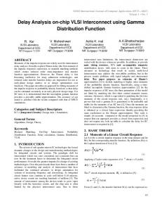
In Kahng’s works, each segment of interconnects is modeled as equivalent RLC circuits. The interconnect trees would be replaced with the RLC network. The first moment and the second moment of transfer function from the source to the sink can be easily figured out by iterative formulas[2]. The accuracy of models is mainly dependent on what the number of segment the interconnect lines are cut into. In the paper, each interconnect line is modeled with ABCD matrix. As we all know, the ABCD matrix of interconnects which derive from telegraphy equations can described interconnect accurately. For an arbitrary interconnect tree, we consider the main path between the source and the sink of interest, and replace each subtree with its respective admittance. To calculate the response at the sink we replace the interconnect line on the main path with ABCD matrix. Fig. 1 shows an example of a main path where every branch on the main path of the tree is replaced with ABCD matrix, and those subtrees off the main path are replaced with their respective admittances. Vn indicates the voltage of node n. VN +1 and V1 indicates the voltage of the source, and the sink respectively. Yn is the admittance of the node n . [ABCD]n is ABCD matrix of the interconnect between node n and n+1.
Abstract - The accuracy of interconnect delay estimations can be improved by the method presented in this paper��in which the first two moments are obtained with ABCD matrix and a stable model to incorporate effects of transport delay into the delay estimate is developed. Simulation results show that the method share the same accuracy with traditional methods when rise time delay is much longer than transport delay and more accurate when the two are of the same order.
I Introduction Elmore delay model based on RC network, still is one of the most popular interconnect delay estimation tools for circuit synthesis and optimization as well as post layout circuit verification, due to its simplicity, recursive properties and ease of adaptation to VLSI interconnect[1]. Elmore delay model uses the first circuit moment which can not capture the effect of inductance of interconnect, to estimate the delay and the accuracy would be deteriorated when clock frequency increases. To achieve higher accuracy, a two-pole model which based on RLC interconnects is presented by Kahng and Muddu[2]. The model based on the first two moments, gains higher accuracy than previous ones due to the second moment capturing the effect of inductance. The transmission line in network of the previous models would cut into several segments and replaced with RC or RLC circuits. However, replacing segments with lumped RC or RLC circuits would lead approximation error to calculate the moments. In the paper, transmission line would be replaced with ABCD matrix which can describe the line accurately. And the accuracy of moment calculation would be improved compared to those previous works. Furthermore, the transport delay is ignored in previous models. Therefore, in this paper, the total delay is divided into the transport delay and the rise time delay. The transport delay must be calculated first and remove its impact from the original system. Then, a stable RLC model is used to approximate the new system to estimate the rise time delay.
VN +2
ª1 «0 ¬
Zs º 1 »¼
VN
ªA «C ¬
Bº D »¼ N
V2
ªA «C ¬
YN
Bº D »¼ 2
V1
ªA «C ¬
Y2
Bº D »¼1
Y1
Fig. 1.�������������������� To calculate the total transfer function of the ladder network, the transfer function between node n and n+1 should be figured out firstly. For a network described by ABCD matrix as shown in Fig. 2, its transfer function can be (1) easily gotten by formula: H n ( S ) = 1/( A + BYn, L ) Yn,in
II. Background
ªA «C ¬
Bº D »¼ n
H n (S)
Fig. 2.
A. Interconnect tree analysis with ABCD matrix
978-1-4244-1922-7/08/$25.00 ©2008 IEEE
VN +1
510
Yn,L
�
6A-5
ª A B º ª cosh(θndn ) Zn,0 sinh(θndn )º «C D» = «Y sinh(θ d ) cosh(θ d ) » � n n n n ¬ ¼n ¬ n,0 ¼
Where Yn , L is the load admittance. To calculate H n ( S ) , Yn , L the sum of the admittance of subtree and the input admittance of post-order network, must be calculated firstly. So it’s necessary to compute the input admittance of the post-order network. Yn ,in = (C + DYn, L ) /( A + BYn , L ) (2)
Where Zn ,o = (rn + ln s) / scn , Yn,0 = 1/ Zn,0 , θn = (rn + sln )scn . rn , ln and cn are the resistance, inductance and capacitance per unit length respectively. Yn , L is the load admittance of the line n and its Talyer expansion is as following Yn, L = yn(0), L + yn(1), L s + yn(2), L s 2 + ... . We expand the transfer function around s=0, and truncate it by only using the first few coefficient of the expansion. Due to the models in the paper are two order models, only the first three coefficient of the expansion would be used to calculate the transfer function. Additionally, we have yn(0),L = 0 according to the characteristic of the practice
H n ( S ) is the transfer function between the node n and n+1. H ( s) is the transform function between the source s and the node N+1 . By using formulas (1) and (2), we can get transfer function of each branch. Then the total transfer function from the source to the sink can be given as following: H (s ) = H s ( s) H N ( s) H N −1 ( s)...H1 ( s ) ������(3) B. Classification of delay
(6) circuits [4]. Then we get YL = y L(1) s + yL(2) s 2 + ... The input admittance Yn,in in the Fig. 2 can be obtained.�
The total delay of interconnects is due to the following two components[3]: (I) the transport delay is due to the time taken for the electromagnetic wave to propagate form source to the destination, and (II) interconnect rise time delay is due to the distributed parameters of the interconnect line. The transport delay for an interconnect line of length h �is given by T E M = h / v ������������������� (4) Where v is the velocity of electromagnetic wave in transmission line. The rise time delay can be given approximately by following formula. TR = kRC = krch 2 ���������������(5)� Where k is constant and R and C are the total resistance and capacitance of the interconnect line. To the interconnect system with transmission line, the unit step response wave is like curve A as shown in Fig. 3. The total delay of interconnect for given threshold voltage is the sum of TEM and TR . The previous models ignored TR would lead big errors when TEM cannot be ignored due to the increasing of the length. As shown in Fig. 3, curve B can hardly match curve A exactly.
Yn , in =
C + DYn , L A + BYn , L
=
Yn ,0 sinh(θ n d n ) + cosh(θ n d n )Yn , L cosh(θ n d n ) + Z n ,0 sinh(θ n d n )Yn , L
�
We expand items of the numerator and denominator. Then the first two coefficient of Yn,in can be obtained easily as (1) following yn,(1) in = Cn + yn , L
yn(2),in =
(1) yn , L Rn C n Rn Cn 2 (2) (1) Rn C n (1) + + y n , L − ( C n + y n , L )( + y n , L Rn ) 3! 2! 2!
(7)
Where Cn = dn cn � Ln = d n ln and� Rn = d n rn The load admittance of each segment is the sum of the admittance of subtree and the input admittance of post-order segment. So the iterative formula can be given as following Yn, L = Yn + Yn −1,in (8) When all of Yn , L are figured out by the formula (7) and (8), the transfer function of each segment can be calculated too. According to the formula (1), the transfer function between Yn and Yn +1 �is given as following H n (S ) =
V
=
Vth
1 cosh(θ n d n ) + Y n , L Z n ,0 sinh(θ n d n )
1 1 + h n (1) s + hn ( 2 ) s 2 + ...
The first two coefficients are obtained as following by expanding the each item of the denominator TEM
hn(1) =
TR
t
Fig. 3.
�
Rn Cn (1) + yn, L Rn 2!
2
hn(2) = Ln2!Cn + (Rn4!Cn )
+ (Ln +
Rn2Cn (1) (2) ) yn,L + yn,L Rn 3!
(9)
H s ( s ) is the transfer function between the source and the node N+1. set Z s = Rs + sLs , 1 H s ( s ) = H N +1 ( s ) = 1 + Z s YN ,in
III. Analysis of New models A. Approximation of transfer function The path from the source to the sink in interconnect tree is regarded as main path, which can be described as a ladder network as shown in Fig. 1. Those interconnect lines on the main path are replaced with ABCD matrix. The ABCD matrix for the transmission line n with length d n can be obtained by solving the telegraphy equations as following:
=
1 1 + Rs y
(1) N , in
s + ( Rs y N(2,)in + Ls y N(1), in ) s 2 + ...
Therefore hN(1)+1 = Rs y N(1),in , hN(2)+1 = Rs yN( 2),in + Ls yN(1),in
511
(10)
6A-5
Real poles. When b12 − 4b2 > 0 �� the two-order system has two different poles. The step response is (1 + a1 p1 ) p 2 p1t (1 + a1 p 2 ) p1 p 2 t u out ( t ) = 1 e + e (18) p 2 - p1 p 2 - p1 2) Complex poles. The condition for complex poles is b12 − 4b2 < 0 � The step response is
The total transfer function
1)
N +1
H (s ) = H s ( s) H N ( s) H N −1 ( s )...H1 (s ) = Π H n (s )
(11)
n =1
Then the first two coefficients of the total transform function can be obtained as following formula h1 =
N +1
¦
n =1
h2 =
h n(1 ) ,
N +1
¦h n =1
(2) n
N + 1 N +1
+¦
¦h
n =1 m =1 n≠m
(1) n
hm(1)
(12)
u out ( t ) = 1 -
B. The stable model concerned with transport delay
Where ρ = tan -1 ( α )
Due to the lumped parameter models can not capture the effect of the transport delay, we divides the delay into two components: the transport delay and the rise time delay. The transport delay of each interconnect segment on the main path between the source and the sink is T f ,n = Ln Cn and can be calculated firstly. Then the total transport delay from the source and the sink is given as following
β
β =
3)
(13)
Since the interconnect system with transmission line is a linear time invariable system, according the feature of transport delay as shown in Fig. 3, we get − sT � then� H *n ( s) = H n (s )esT �����(14)� H n ( s ) = H n * ( s )e Substitute� H n ( s ) �into the formula (11) and expand the numerator and denominator of formula (13) as following� H * (s ) = e
sT f
N +1
Π H n ( s) =
n =1
Double poles. The condition for a double pole is b12 − 4b2 = 0 ��The step response is
kakng
1
2
approximate the transfer function H ( s ) in Kahng’ model, To compare the Kahng model with the new model objectively, the delay would be calculated with MATLAB by using the step response formulas rather than the closed formula derived by Kahng.�
(15)
Where k1 = T f 㧧 k2 = (T f )2 / 2 㧧 h1 and h2 can be obtained from the formula (10). The first two moments are expressed as following M 1 = h1 - k1 , M 2 = k 2 - k1h1 + h12 - h2 (16) Due to the resistance of interconnect on chip or MCM have dominate impact on the delay, in the most case we can get[4] M 1 and M 2 are both more than zero. After T f
IV. Experimental Results and Discussion A. Example 1
is removed from H (s ) , we get the new transfer
In Fig. 4, a interconnect system with transmission line is shown. r = 15 kΩ/m, l = 246 nH/m and c = 176 pF/m are the resistance, inductance and capacitance per unit length respectively. Rs ޔLs ޔCT and h are source resistor, source inductor, load capacitor and length of line. Input signal is unit step signal and the delay estimates refer to 50% threshold voltage. In the experiment, simulations would be made by the new model and the Kahng’ model separately, and compare those results with those simulated by Hspice which can provide accurate results. In the Table I, the 50% delay of 3mm interconnect line are calculated under the different source impedance and load admittance. In the table 2, the 50% delay at different length are given when Rs = 50 Ω ޔLs = 2.46 pH and CT = 0.176 pF.
function H * ( s) . When we use few moments to describe the system, actually the transfer functions are truncated and may lead the instability. So some tactics should be used to deal with the situation. In the paper, we would use a two-order model to approximate H* (s) , which is described as following
H app ( s ) = (1 + a1 s ) /(1 + b1 s + b2 s 2 )
.
2 (b2 - a 2 )
according to the sign of the� b12 − 4b2 . In experiments of the paper, we would not use the closed formula to estimate the rise time delay, but calculate the delay directly by match tool MATLAB. H ( s ) = 1 /(1 + b s + b s 2 ) �is used to
f ,n
1 + k1 s + k 2 s 2 + o( s 2 ) 1 + h1 s + h2 s 2 + o ( s 2 )
4 ( b 2 - a 2 ) - b12
For the given threshold voltage Vth � we select the formula (18), (19) or (20) to estimate the rise time delay TR
n =1
f ,n
-b1 2(b2 - a2 )
α=
uout (t ) = 1- e p1t + ( p1 + a1 p12 )tetp1 ������������(20)
N
Tf = ¦ Tf ,n
α 2 + β 2 -α t a (α 2 + β 2 ) -α t e sin( β t + ρ ) + 1 e sin( β t ) (19) β β
(17)
Where a1 = M 2 / M 1 , b1 = M1 + M 2 / M 1 , b2 = M . The first two moments of the new system equal those of H * ( s) , besides the stability of the new system can be guaranteed [6]. The two poles p1,2 as following are derived from the equation (17). We assume that the input signal is the step signal, and TR is the rise time delay referring to the 2 1
threshold voltage Vth . Depending on the sign of b12 − 4b2 , the poles of the transfer function can be real or complex. We derive delay estimation formulas separately from the two-pole response for each of these cases.
Fig. 4.
512
6A-5
TABLE IV The changed parameters under different conditions
TABLE I 50% delay of different source and load Spice
Source Rs
Ls
/Ω 40 50 75 40 50 75
/pH 2.46 2.46 2.46 2.46 2.46 2.46
Load CT /pF 0.176 0.176 0.176 1.76 1.76 1.76
/ps 33.9 38.9 51.9 130 145 184
Delay Model Kahng New Model Td Error Ttotal Error /% /ps /ps /% 39.9 17.7 36.3 7.07 44.1 15.1 40.6 6.01 54.8 5.58 52 0.19 133 2.31 130.7 0.54 148 2.07 145.7 0.48 187 1.63 184.7 0.38
Cond. Cond1 Cond2
Spice
/mm 0.1 0.5 1 1.5 2 2.5 3
/ps 7.08 10.5 14.9 19.9 24.4 31.6 38.3
Delay Model/ps Kahng New Model Td Error Tf TR Ttotal /ps /% /ps /ps /ps 7.1 0.28 0.66 6.41 7.07 11.3 7.62 3.29 7.55 10.8 17 14.1 6.58 9.32 15.9 23.1 16.1 9.87 11.5 21.4 29.5 20.8 13.2 14.2 27.2 36.6 15.8 16.4 17.3 33.7 44.1 15.1 19.7 18.9 40.6
W4 /mm 1 3
W6 /mm 3 3
Ct1 /pf 0.176 0.176
Ct2 /pf 0.176 0.176
Ct3 /pf 0.176 0.176
Ct4 /pf 0.176 0.176
Ct5 /pf 0.176 0.176
According to the data in the Table I, we can find the model in the paper is more accurate than Kahng’s model with the source and load changed when the length of interconnect is large. The main problem of previous lumped parameter models is that their can not capture the transport delay, and the accuracy of estimation would be deteriorated when the transport delay increase, just as shown in the Table II. From the data of the Table II, we can also find that the accuracy of the new model would not deteriorate with the increasing of length as the Kahng’s model. The Table III the simulation results of respective nodes of a interconnect tree under different conditions. From the data of the Table III, we can also figure out that when the transport delay and the rise time delay are of same order, the accuracy of estimations would be improved, such as the node 6.
TABLE II 50% delay in different length
h
W1 /mm 1 2
Error /% 0.14 3.33 6.71 7.39 11 6.64 6.01
V. Summary and Conclusions The accuracy of interconnect delay predictions in integrated circuits can be improved by RLC model presented in this paper. In the model, the moments are derived form ABCD matrix firstly. And then the total delay is divided into two components: the transport delay and the rise time delay, to estimate. Simulation results show that the method has the same accuracy with traditional methods when the transport delay is much smaller than the rise time delay and is more accurate when the two are of the same order.
B. Example2 As shown Fig. 5, the interconnect tree is uniform, and r = 15 kΩ/m, l = 246 nH/m and c = 176 �pF/m are the resistance, inductance and capacitance per unit length. The load capacitances of sinks are list in the Table III. The lengths of interconnect line W2, W3, W5, W7 and W8 keep unchanged under different conditions and is 1mm. The rest interconnect lines in the figure are list in the Table II. The delay estimates refer to 50% threshold voltage.
References [1] W. C. Elmore, “The transient response of damped linear networks with particular regard to wideband amplifiers”, Applied physics, Vol. 19, pp.55-63, 1948. [2] A. B. Kahng, S. Muddu, “An analytical delay model for RLC interconnects”, IEEE Trans on computer-aided design of integrated circuits and system, Vol. 16, pp. 1507-1514, 1997. [3] X. D. Yang, C. K. Cheng, W. H. Ku, et al. “Hurwitz stable reduced order modeling for RLC interconnect trees”, IEEE Journal of Analog Integrated Circuits and Signal Processing, Vol. 31, pp. 222-228, 2002. [4] Peter R. O’Brien, Thomas L. Savarino, “modeling the driving-point characteristic of resistive interconnect for accurate delay estimation”, ICCAD, pp.512-515, 1989. [5] Y. I. Ismail, E. G. Friedman, J. L. Neves, “Equivalent Elmore delay for RLC trees”, IEEE Trans on CAD, Vol. 19, pp.83-97, 2000. [6] B. Chen, H. Z. Yang, et al., “Stable interconnect RC model via matching the first Two moments”, Communications, Circuits and Systems and West Sino Expositions, Vol. 2, pp. 1330-1333, 2002.
Fig. 5. TABLE III 50% delay of interconnect trees Cond.
Cond1
Cond2
node /mm
4 5 6 7 8 4 5 6 7 8
Spice
/ps
120 133 150 130 130 179 180 194 175 175
Kahng Td /ps 116 137 163 129 129 201 195 221 188 188
Delay Model /ps New Model
Tf
TR
Ttotal
/ps 13.2 19.7 32.9 19.7 19.7 32.9 26.3 39.4 26.3 26.3
/ps 103.1 115 119 109 109 154 163 167 158 158
/ps 116.3 134.7 151.9 128.7 128.7 186.9 189.3 206.4 184.3 184.3
513