Mar 13, 2007 - James-Roxby et al. [6] present architectures that use shared memory only for data, while multiple programs must reside locally in the processor ...
A Design Kit for a Fully Working Shared Memory Multiprocessor on FPGA Antonino Tumeo Matteo Monchiero Gianluca Palermo Fabrizio Ferrandi Donatella Sciuto Politecnico di Milano, Dip. di Elettronica e Informazione
{tumeo,monchier,gpalermo,ferrandi,sciuto}@elet.polimi.it
ABSTRACT
Nevertheless, implementing a multiprocessor on FPGA incurs in many additional problems. Most of these issues, like cache coherence, multiprocessor interrupt management, processor identification and synchronization are left to the system designer. This paper tries to give an answer to this problem, presenting a platform which makes it easy to design a multiprocessor on FPGA. We introduce a synthesizable architecture and a programming model. These two elements permit to easily write parallel applications, and make them run on a commercial FPGA. Main contributions can be summarized as follows: 1) An architecture of a shared memory multiprocessor. This is composed by commercial IPs, organized in a parametric framework. Threading/synchronization features are exposed to the programmer by a micro-OS kernel. 2) A programming model, which exposes parallelism of multimedia applications. 3) A software mechanism to deal with data consistency, and a hardware layer to manage thread synchronization. We implemented this framework by using the Xilinx toolset and a complete JPEG encoder application, which have been written by using our programming model. Experimental results show that the parallelized application, running on our system, and implemented with 4 simple softcores, achieves the same performance of a hard-processor. The structure of this paper is the following. Section 2 discusses some related work. The proposed architecture is described in Section 3. Section 4 presents the programming model. Experimental results are discussed in Section 5. Finally, Section 6 concludes the paper.
This paper presents a framework to design a shared memory multiprocessor on a programmable platform. We propose a complete flow, composed by a programming model and a template architecture. Our framework permits to write a parallel application by using a shared memory model. It deals with the consistency of shared data, with no need of hardware coherence protocol, but uses a software model to properly synchronize the local copies with the shared memory image. This idea can be applied both to a scratchpadbased architecture or a cache-based one. The architecture is synthesizable with standard IPs, such as the softcores and interconnect elements, which may be found in any commercial FPGA toolset.
Categories and Subject Descriptors C.1.4 [Parallel Architectures]: Distributed architectures
General Terms Design
Keywords FPGA, shared memory, reconfigurable logic, programming model, embedded computing
1.
INTRODUCTION
Chip Multiprocessing (CMP) represents a new paradigm for processor design. This trend has been pursued by most semiconductor industries, both for high performance computers (e.g. the IBM Cell), and complex embedded systems (e.g. ST Nomadik and Philips Nexperia). Reconfigurable platforms have emerged as an important alternative to ASIC design, featuring flexibility versus relatively lower performance [10]. Recently, most FPGA vendors (e.g. Xilinx and Altera) have shipped synthesis infrastructure, including softcores and interconnect elements.
2.
RELATED WORK
Several works discussing multiprocessor systems implemented on FPGA have appeared. Clark et al. [2] and James-Roxby et al. [6] present architectures that use shared memory only for data, while multiple programs must reside locally in the processor memory. Furthermore, ad hoc programming techniques are used to deal with synchronization of shared resources, lacking of a real systematic approach. Although Altera provides a simple mutex core to address synchronization problems, Gai et al. [4] propose a dedicated arbitrator using the G-T algorithm with its related API. Anyway they do not address the cache coherency problem and do not show any performance benchmark. Hung et al. [5] focus their attention on the cache coherence problem, proposing a dedicated hardware module able to snoop memory writes. Since the mechanism uses interrupts to in-
Permission to make digital or hard copies of all or part of this work for personal or classroom use is granted without fee provided that copies are not made or distributed for profit or commercial advantage and that copies bear this notice and the full citation on the first page. To copy otherwise, to republish, to post on servers or to redistribute to lists, requires prior specific permission and/or a fee. GLSVLSI’07, March 11–13, 2007, Stresa-Lago Maggiore, Italy. Copyright 2007 ACM 978-1-59593-605-9/07/0003 ...$5.00.
219
the applications resides on the external DDR memory, while private data are saved in the local memories. The processor core can be further configured with a local data cache for the shared data segment.
3.1
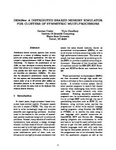
Figure 1: The CerberO Architecture validate the cache, it may suffer of performance problems and, with non-precise interrupt management, it cannot in our opinion always ensure the correctness of the operation. Recently, Gaisler Research AB has presented LEON 3 [1], a synthesizable VHDL model of a processor compliant with the SPARC V8 architecture with full symmetric shared memory multiprocessing support, comprehensive of cache coherence, but no hardware synchronization. This is possible thanks to the open source nature of the LEON project, while it would not possible for the MicroBlaze and NIOS softcores, by Xilinx and Altera, respectively. Furthermore, the LEON core is quite complex, making it difficult to implement more than one instance on a medium size FPGA. Consistency models are deeply discussed in [3]. In addition, explicit software coherency mechanisms have been proposed several times in the past. In particular, we mention the recent paper by Loghi et al. [7] that evaluates and suggests software coherency as a solution when looking for favorable power/performance ratios, in the context of Multiprocessor System-on-Chip.
3.
Synchronization and Communication
Synchronization and Processor Identification mechanisms are supplied by a dedicated module, the Synchronization Engine (SE). This is connected to each processor through the Fast Simplex Link (FSL) point-to-point connections. This module is composed of three different memories and provides hardware locks and barriers management. The first memory is a 32 bit Context Access Memory (CAM) able to store the addresses of shared locations. Since, in the Xilinx toolchain, IP Cores are accessed through memory mapped calls, this memory can also store addresses of shared peripherals. The second memory is a RAM that stores the id of the processor that currently retains a lock or that has initialized a barrier. The third memory, another RAM, is used for hardware barrier management to count the arrivals (through a decrementing counter) of the processors to the barrier. When the stored value reaches zero, the processors are released and go on executing. Locks and barriers requests are served in a FIFO ordering, and, when two contemporary requests occur, a static priority ordering kicks in. When a processor requests a lock, that is already acquired by another MicroBlaze, or when it is waiting on a barrier, it starts spinning in a busy-waiting loop. The number of slots for locks can be configured by the system designer considering the target application and the number of processors of the target CerberO architecture. We implemented a simple crossbar to permit high bandwidth direct point-to-point communication from and to each processor in the system to allow fast small data passing without adding pressure to the shared bus and the shared memories. This module (CerberO CrossBar) is connected to a second FSL master/slave couple of ports on each processor.
3.2
Task Scheduling and Allocation
Both the SE and the CrossBar provides the necessary features to enable the CerberO Nano Kernel (CNK), our thin software layer that permits to schedule and dynamically allocate threads on the processors of the architecture. CNK relies on two shared tables that contains the ready tasks and the free processing elements. First operations consist of a boot phase, which selects one MicroBlaze to be the master processor, and inserts the first threads in the ready table. The master processor starts sending to the other ones the addresses of the tasks to execute over the CrossBar. Then, any processor can start adding a new task to the ready task table and, if there are any other free processors (reported in the free processors table), it directly sends them the address of the thread to execute. When the execution of a task ends, the processor checks if there are any other ready tasks. If this is not the case, it sets itself as free and waits for the address of a new thread to come from the CrossBar. We currently adopt a run to completion model for each task. It’s important to note that all these components can be easily integrated in the common EDK flow, in order to permit fast prototyping of multiprocessor system-on-chip. In addition, the system is easy to augment with application specific IP Cores, private or shared among all processors.
ARCHITECTURE
The CerberO Architecture has been implemented using the commercial standard Xilinx Embedded Developer Kit (version 8.2) and its toolchain. CerberO, showed in Figure 1, is realized connecting multiple Xilinx MicroBlaze softcores on a single shared Coreconnect On-Chip Peripheral Bus (OPB). Shared IPs and the controller for the shared external memory reside on the OPB bus. The shared IPs include the UART controller, the Debug Module for the processors, the SysACE controller for the compact flash reader, a small shared Block RAM memory for booting purposes and a timer to record execution times. The external memory controller is a slightly modified version of the standard Xilinx MultiChannel OPB DDR RAM controller, augmented to support up to eight Xilinx CacheLink ports instead of the standard four ports, in order to implement up to eight MicroBlaze cores with instruction caches active. Each MicroBlaze in the system is connected to a local memory through the Local Memory Busses (LMB) for private data. The shared instruction and data segments of
220
Pn
Virtual addressing space
Machine physical addressing space mapping on physical DRAM and FPGA RAM
to deal with this problem, which relies on the partitioning of the program induced by synchronization operation. In the following, we make several assumptions about the hardware (consistent with the architecture of Section 3). Flush primitives are provided to write in main memory data imported in the private memories/caches. The consistency model we assume is specified as follows: Synchronization data are always consistent. All the other data are consistent only at each synchronization point. It can be classified as a Weak Ordering model, mainly because it breaks the write atomicity property [3] – i.e. writes to shared data are not seen in the program order, since these can be locally elaborated while being incoherent in the shared memory. As we have seen in Section 3, synchronization is handled by the SE, thus ensuring sequential ordering for synchronization variables. For other data, the programmer must be aware to protect contended structures with locks. At a first glance, the model may appear strict. Nevertheless, many programs can be written using this model, still being performing. This especially applies to array-based applications, often parallelized by dividing large matrices into smaller portions, which are then assigned to the processors.
P2 DRAM
P1 P0
Shared portion of address space portion SharedShared portion of address of address space Shared portionspace Private portion of of address space Private portion of address space Private portion of address spaceof Private portion address space
Pn
Mn P1
P2
M2
P0
M0
M1
FPGA
Figure 2: Addressing space
4.
PROGRAMMING MODEL
The programming model we propose permits to easily write parallel applications for the architecture described in Section 3. Most of its features has been inherited from conventional parallel programming model for scientific computation, like for example ANL PARMACS [8] and OpenMP [9]. It well adapts to array-based multimedia applications, like image and video processing.
4.1
5.
CerberO has been used to prototype a complete multimedia application from start to end, file reading and saving included. The application implements the baseline JPEG compression algorithm with Huffman coding and is composed by seven phases: (i) original image (.PPM format) reading, (ii) RGB to YUV color spaces conversion (for color images), (iii) expansion, (vi) downsampling, (v) quantization tables setting, (vi) bi-dimensional Discrete Cosine Transform (DCT 2D), Quantization and zig-zag reordering, (vii) entropic coding and file saving. Sequential phases are (i), (iii) and (vii), while the other phases can be easily parallelized. In particular, since the RGB to YUV conversion works independently pixel for pixel, it’s possible to distribute the workload following different patterns. The downsampling phase works instead averaging the Chroma information for four adjacent pixels. DCT 2D, quantization and zig zag reordering then executes on blocks of 8 x 8 pixel. Our experiments have been conducted using a 160x120 .PPM image, as input data set. We decided to spawn multiple threads working on 8x8 blocks for all the parallel phases and to flush the shared data in private memories before joining and re-spawning successive threads. Data are loaded into the local memory at the beginning of each phase (loading local data is automatic for CerberO with caches). At the end of each phase, private data are synchronized with shared data. This operation (‘flush’) is similar for the architecture with local caches and local memories. We synthesized three different architectures implementing from 2 to 4 MicroBlaze soft cores following our framework and downloaded onto a Xilinx University Program VirtexII Pro Development Board, which features a Virtex-II Pro XC2VP30 Speed Grade -7 FPGA. Their occupations, compared to a single MicroBlaze platform are shown in Table 11 . The MicroBlaze soft processors have been implemented with barrel shifter, integer divider and pattern comparator.
Memory Model
As shown in Figure 2, the addressing space of each processor is partitioned into a private portion and a shared portion. The private space is accessible only by the local processor, while the shared one is equally seen by all components of the system. Function stack is kept into the private space. Any datum can be mapped into the shared space by using a special dynamic allocation primitive. Software allocation primitives can be used to move data from the shared space to the local memory and vice versa. Since in a FPGA softcore, like the MicroBlaze, data caches are implemented with the same internal Block RAMs of the private data memory, the latencies of a local cache or a local memory are similar. For this reason, our system can be configured either with data cache or local memories, and the programming model can be specialized accordingly. The use of a cache or a local memory does not theoretically change the problem so much, for the programming model. Data in the local memory must be explicitly moved in and out (we actually copy shared data to local variables and vice versa), while the data cache automatically load and writes data, but needs a coherence protocol. Since we choose not to implement a hardware protocol, we must rely on explicit flushes, which are similar to explicit data movement from the local memory to the shared memory.
4.2
Execution Model
Thread execution is based on a fork/join model, similarly to PARMACS and OpenMP. Inter-thread synchronization is achieved through barriers and locks.
4.3
EXPERIMENTAL RESULTS
Consistency Model
The consistency of local data (either cached or stored to a local memory) is not enforced by the hardware. So, proper commands for loading and flushing of shared data must be explicitly inserted in the program. We propose a strategy
1
221
The architecture with data caches or local memories have
3
Table 1: FPGA utilization of the different architectures
4 input LUTs Slice FFs
27392 27392
1P 15% 11%
CerberO 2P 3P 31% 44% 22% 30%
Normalized Execution Time
Total
2.5
4P 58% 38%
2 1.5 1 0.5 0 D$
LM
1MicroBlaze
Since the PowerPC architecture does not feature a Floating Point Unit, we configured the MicroBlaze without it. For each MicroBlaze processor the instruction cache is 8 KB, while the private local memory is 32 KB. The data cache, when enabled, is 8 KB. All the CerberO systems have been synthesized at 50 MHz. We also synthesize a PowerPC platform, running at 100 MHz, which uses instruction and data caches of 16 KB. The PowerPC consists of the hard core processor present on the Virtex II-Pro FPGA and the necessary buses and controllers for memories and the mass storage device. Figure 3 shows the performance results measured on our board for 1, 2, 3, 4-core CerberO, normalized with respect to the PowerPC. You can see that the execution time linearly scales with the number of cores. This proves the efficacy of our parallelization and multiprocessing platform. The performance of the single-MicroBlaze architecture for the RGB to YUV and DCT 2D phases is significantly poor with respect to the PowerPC (5X and 5.6 slowdown, respectively). This happens because these phases are especially computationally intensive. Thanks to the parallelization the gap can be reduced up to 20% (RGB to YUV) and 25% (DCT 2D). When comparing the solution with the data cache and the local memories, it can be seen that the latter is better by 14%, 9%, 7%, and 5% for 1,2,3,4 cores. This is not due to the size of the local memory (4X w.r.t. the cache), but to the fact that the local memory avoids misses due to conflicts and write-through. This advantage decreases with the number of cores, because the size of the working set of each cache gets reduced and the number of conflicts in the cache gets smaller too. In general, CerberO with 4 cores and the local memories is only 12% slower than the PowerPC. Notice that the PowerPC is an ASIC running at 100 MHz, while our FPGA does not allow us to synthesize CerberO at more than 50 MHz.
6.
Read
RGB to YUV
D$
LM
2MicroBlaze Downsample + expansion
D$
LM
3MicroBlaze Set quantization tables
D$
LM
PPC
4MicroBlaze DCT 2D + Quantization
Entropic coding + write
Figure 3: Performance evaluation for CerberO w/ data caches or local memories, and PowerPC can achieve comparable performance of a more performing hard-processor.
7.
REFERENCES
[1] Leon3 Processor. available at http://www.gaisler.com. [2] C. R. Clark, R. Nathuji, and H.-H. S. Lee. Using an fpga as a protyping platform for multi-core processor applications. In Workshop on Architecture Research using FPGA Platforms, 2005, 2005. [3] A. G. David E. Culler, Jaswinder Pal Singh. Parallel Computer Architecture: A Hardware/Software Approach. Morgan Kaufmann, 1999. [4] P. Gai, G. Lipari, M. Di Natale, M. Duranti, and A. Ferrari. Support for multiprocessor synchronization and resource sharing in system-on-programmable chips with softcores. In SOC Conference, 2005. Proceedings. IEEE International, pages 109–110, Sept. 2005. [5] A. Hung, W. Bishop, and A. Kennings. Symmetric multiprocessing on programmable chips made easy. Design, Automation and Test in Europe, 2005. Proceedings, pages 240–245, 2005. [6] P. James-Roxby, P. Schumacher, and C. Ross. A single program multiple data parallel processing platform for fpgas. 2004. FCCM 2004. 12th Annual IEEE Symposium on Field-Programmable Custom Computing Machines, pages 302–303, 2004. [7] M. Loghi and M. Poncino. Exploting energy/perfomance tradeoffs in shared memory mpsocs: snoop-based cache coherence vs. software solutions. In Design, Automation and Test in Europe, 2005. Proceedings, 2005. [8] E. L. Lusk and R. A. Overbeek. Use of monitors in fortran: a tutorial on the barrier, self-scheduling do-loop, and askfor monitors. In on Parallel MIMD computation: HEP supercomputer and its applications, pages 367–411, Cambridge, MA, USA, 1985. Massachusetts Institute of Technology. [9] OpenMP. OpenMP application program interface. Version 2.5, May 2005. Available at http://www.openmp.org. [10] F. Vahid. The softening of hardware. Computer, 36(4):27–34, 2003.
CONCLUSIONS
Implementing a shared memory multiprocessor on FPGA imposes several problems. Hardware cache coherency algorithms are complex to implement and verify. Furthermore, commercial toolsets typically provide IPs designed for singleprocessor systems, and make it difficult to organize them in a multiprocessor. In this paper, we propose a multiprocessor architecture, and a programming model to easily write and run parallel multimedia applications. We used this framework to implement a 4-processor system, executing a JPEG encoder. The experiments show that our multiprocessor architecture approximately the same occupation, since both the data cache and the local memory are implemented with the BRAM blocks.
222


![Memory Consistency Models for Shared-Memory - CiteSeerX [PDF]](https://m.moam.info/img/260x300/memory-consistency-models-for-shared-memory-citese_64d8c39a098a9e2e618b4666.jpg)


