1
A Design Workflow for Dynamically Reconfigurable Multi-FPGA Systems Alessandro Panella∗ , Marco D. Santambrogio†‡ , Francesco Redaelli† , Fabio Cancare† , and Donatella Sciuto† ∗ Computer Science Department - University of Illinois at Chicago, Email:
[email protected] † Dipartimento di Elettronica e Informazione (DEI) - Politecnico di Milano, Email: {santambr, cancare, fredaelli, sciuto}@elet.polimi.it ‡ Computer Science and Artificial Intelligence Laboratory - Massachusetts Institute of Technology, Email:
[email protected]
Abstract—Multi-FPGA systems (MFS’s) represent a promising technology for various applications, such as the implementation of supercomputers and parallel and computational intensive emulation systems. On the other hand, dynamic reconfigurability expands the possibilities of traditional FPGAs by providing them the capability of adapting their functionality while still running to cope with runtime environment changes. These two research directions are merged together in this work, that describes a methodology for designing dynamic reconfigurable MFS’s. In this paper a novel MFS design flow has been described, which makes use of blocks reuse through dynamic reconfigurability to make the implementation of large systems feasible even on multi-FPGA architectures with strict physical constraints. Functional to this goal is the development of an algorithm for the extraction of the isomorphic structures of a circuit that extensively exploits the hierarchy of the design.
I. I NTRODUCTION The use of Field Reprogrammable Gate Arrays (FPGAs) is nowadays widespread in both industry and academic research. Their computational power can be increased through the creation of clusters of chips. Besides obviously augmenting the available physical area, this also provides the possibility of massively exploiting parallel computation. Such multiFPGA systems (MFS’s) are currently used in supercomputing applications and logic emulation of custom circuits [1]. A computational paradigm attracting growing interest is reconfigurable computing (RC). An early definition given by Gerald Estrin refers to RC as the process of altering the location or the functionality of a system element, as a response to faults, changes in the environment or explicit application needs [2]. Due to their reprogrammability, FPGAs currently represent the leading technology for implementing reconfigurable systems. In recent years, the evolution of FPGA architectures has made it possible to further increase the degree of flexibility in the use of such chips. This innovation is represented by the possibility of having parts of the FPGA reconfigured at run-time, while others are still running, so that the execution of the system never ceases. This technique is called partial dynamic reconfigurability, as opposed to the standard static reconfigurability. A number of works about MFS design can be found in literature (e.g. [1], [3]–[5]), but only few approaches have been proposed that explore the field of dynamically reconfigurable MFS’s ([6], [7]). Merging together the potential of MFS’s and reconfigurability is nevertheless
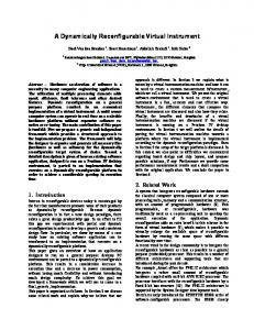
a promising research direction. Although the area available on MFS’s is usually large, some complex applications may require even more space, thus imposing the replacement of the physical architecture with a larger one, a process that is very expensive and time-consuming. By providing a larger virtual area, dynamic reconfigurability allows to go beyond the physical space constraints of the architecture [8]. The presented work proposes a novel design methodology that exploits the dynamic reconfigurability of interconnections in MFS’s. This allows design blocks of the application to be used more than once during execution, with the result of significant area savings. At the best of our knowledge, no other work on multi-FPGA design has explored this scenario. The remainder of this paper is organized as follows. Sections II, III, and IV present the proposed MFS design workflow and describe in details the three phases it is composed of. Section V provides the obtained experimental results, while Section VI briefly reports previous works on MFS design, comparing them with the proposed methodology. Section VII concludes the paper providing some hints for future work. II. P ROPOSED W ORKFLOW AND D ESIGN E XTRACTION The approach proposed in this paper consists of a workflow for the design of MFS’s, whose abstract view is represented in Fig. 1 and is briefly described in the following.
VHDL
Application Description
Design Extraction Global Physical Layout
Multi-FPGA Architecture Description
Output files
Reuse & Dynamic Reconfiguration
no
Feasible?
yes
Figure 1.
Outline of the proposed multi-FPGA systems design workflow.
The input of the design process consists of a VHDL description of the application and a specification of the target
2
multi-FPGA architecture. The VHDL code undergoes a design extraction phase, which aims at collecting the information relevant to the design structure. A global physical layout phase performs the partitioning, placement and routing of the application on the specified architecture. At this point, two situations are possible. If the application fits into the architecture, the flows ends. Otherwise, another step is undertaken, aimed at exploiting the dynamic reconfiguration of the communication infrastructure for modules reuse. The output of the workflow is a new VHDL specification, describing the modules to be instantiated on each FPGA, together with information about the reconfiguration of interconnections. This process relies on existing commercial tools (e.g. Xilinx ISE) for subsequent intra-FPGA synthesis.
slices is retrieved by this step, using existing FPGA synthesis tools such as Xilinx XST [9]. Each leaf of the extracted hierarchical tree is then constituted by a single VHDL process or a group of data-flow instructions. The granularity of this structure is quite coarse, especially if compared to usual gate-level netlists. The choice of handling the circuit at a process-level granularity arises from the fact that the presented workflow performs a global mapping of the application on a multi-FPGA architecture, with subsequent phases taking care of fine-grained local syntheses. In this context, dealing with a low number of relatively large design modules leads to faster results.
A. Intermediate Representation
The global layout phase deals with the search of a feasible mapping of the parsed application on a multi-FPGA architecture received as input, while optimizing some objectives, i.e. the interconnections length. Such mapping assigns one and only one host FPGA of the architecture to each leaf block of the input application and routes interconnections between any two communicating modules assigned to different chips. The cost function to be minimized is the estimated length of the interconnections between blocks assigned to different FPGAs, measured in number of hops and weighted over connections width. Let us define w(i, j) as the amount of communication in number of bits between nodes i and j and let ci identify the FPGA node i is assigned to. The cost function to be minimized is the Weighted Estimated Wire Length (WEWL), computed as follows: X W EW L = w(i, j)d(ci , cj )
The VHDL specification received as input is parsed and interpreted, and the result is saved in a specifically designed intermediate representation, that maintains information both on the structure and the hierarchy of the design tree-like data structure. Hierarchy information is useful to our task for two important reasons. The first one depends on what makes the designer choose a particular design hierarchy when implementing the VHDL application. The designer follows some simple implicit rule in recursively aggregating – or splitting down – components. Design blocks are built based on their functionality: if two sub-components (children) carry out operations that are theoretically portions of a larger function, they are likely to be aggregated in a bigger component (parent). It is evident that such sub-components are probably strongly interconnected. Therefore, it seems natural and favorable to exploit this information in the partitioning, placement and routing of the input circuit. The second reason is rooted in the concept of regularity: if two components belong to the same type, they are roots of two identical sub-trees in the hierarchy. Therefore, when a given operation is carried out during the execution of some algorithm in one of these subtrees, it can be immediately replicated in the other one. B. VHDL Preprocessing and Extraction The extraction phase is composed of two steps. First, the VHDL specification is preprocessed to reduce it to a pure VHDL structural description. The resulting code contains only structural statements for the intermediate nodes of the hierarchical tree, while behavioral and data-flow instructions are allowed exclusively in leaf blocks. To obtain a pure structural description, two operations are carried out for each component in the design: 1) For every process, a leaf component is created which contains the process. The process in the original file is replaced by the instantiation of this component. 2) All data-flow instructions are turned into a leaf component, and are replaced by the instantiation of such component. Then, the specification is parsed into the intermediate representation. The estimated FPGA area occupation in number of
III. G LOBAL P HYSICAL L AYOUT
1≤i