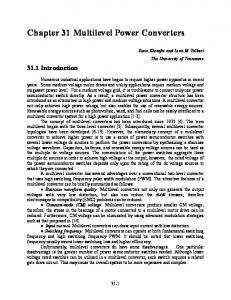
International Journal of Engineering, Science and Technology Vol. x, No. x, 2010, pp. xx-xx
MultiCraft
INTERNATIONAL JOURNAL OF ENGINEERING, SCIENCE AND TECHNOLOGY www.ijest-ng.com © 2010 MultiCraft Limited. All rights reserved
A DSP based SPWM technique for multilevel inverter M.M.Renge1*, H. M. Suryawanshi2 1*
Department of Electrical Engineering, Shri Ramdeobaba Kamla Nehru Engineering College Nagpur (M.S), India 440013 2 Department of Electrical Engineering, Visvesvaraya National Institute of Technology, Nagpur (M.S), India 440011 * Corresponding Author: e-mail:
[email protected], Tel +91-712-2582844, Fax. +91-712-2583237
Abstract In recent years, industry and utility have began to demand high power rating, and multilevel inverter topologies have become a solution for high power application. Various modulation techniques are developed to control the multilevel inverter. Carrier based sinusoidal pulse width modulation (SPWM) is more popular due to its simplicity but this technique requires many timer or combination of digital signal processor (DSP) and field programmable gate array (FPGA) for multilevel inverter. This paper presents the realization of SPWM technique using single low cost DSP. The computational time required to DSP is small which makes it suitable for real-time implementation and DSP has sufficient time to perform other tasks. Experimental results on threephase five-level diode clamped inverter are presented to confirm the validity of proposed idea. Keywords: Sinusoidal pulse width modulation, multilevel inverter, DSP 1. Introduction In response to growing demand for high power inverter unit, multilevel inverter have been attracting attention from academic as well as industry in last three decade. Multilevel inverter is a power electronic device built to synthesize a desired ac voltage from several levels of dc voltages. Compared with traditional two-level voltage inverters, the primary advantages of multilevel converters are their smaller output voltage steps, which result in higher power quality, lower harmonic components, higher voltage capability, better electromagnetic compatibility, and lower switching losses (Nabae et al , 1981, Rodriguez et al. , 2002). A multilevel inverter not only achieves high power rating, but also enables the use of renewable energy sources (Peng and Lai, 1997). Further, they have similar dynamic properties as two level converters with comparable switching frequencies. Hence, these are suitable for flexible ac transmission system (FACTS), high voltage custom power applications and for distributed power systems (Soto and Green, 2002, Woo, 2001). The multilevel inverter starts from three levels. As the number of level increases, the synthesized output waveform adds more steps, producing a staircase waveform. This output voltage waveform approaches to the sinusoidal waveform as a number of levels increase. With good trade off between complexity of implementation and superiority in performance, a multilevel inverter is mostly chosen to be three to nine levels. Three-level diode clamped inverters are in use ( Binu, 2006) and five-level inverter is extensively studied in literature (Rodriguez et al, 2002, Menzies et al 1994, Renge and Suryawanshi, 2008). Several different pulse width modulation techniques for multilevel inverters have been proposed (Czarkowski, Liu, Pillay, 2000, Carrara et al 1992, Gupta and Khambadkone 2007, Loh and Holmes, 2002) with primary goal of synthesis a desired set of ac voltage waveform. The secondary goal is the shaping harmonics spectrum of the output voltage and current waveform. Out of various multilevel PWM methods, carrier-based PWM method and space vector PWM (SVPWM) technique are mostly used to control the multilevel inverter. SVPWM has better THD performance where as SPWM is superior to SVPWM for five-level converter and above, because implementation is simple. In SPWM technique, triangular carrier based modulation scheme have been studied quite extensively from the point of view of harmonics characterization (McGrath and Holmes, 2002). Four carrier phase disposed or phase shifted waveforms are required for five-level inverter. Theoretically, several variation of basic technique, which utilizes disposition of the triangular carrier waveform to shape the high frequency harmonics spectrum have been proposed (McGrath and Holmes, 2002). Traditional natural SPWM system employs analog control system. Analog control relies on large number of discrete component resulting high cost with
2
Renge et al./ International Journal of Engineering, Science and Technology, Vol. 1, No. 1, 2010, pp. xx-xx
Five level diode clamped inverter Vdc 4
Sa1
Sb1
Sc1
Induction motor
Vdc 4 0
Va
Vb Vc
Vdc 4 Vdc 4
Sa8
Driver circuit
Sb8
Sc8
DSP TMS320F2812
Figure 1. Proposed scheme DSP controlled three-phase Five-Level Diode Clamped inverter Vdc/2 C4 Vdc/4 C3 0 C2 -Vdc/4 C1 -Vdc/2
r4 r3 r2 r1
Figure 2. PD carrier, reference waveform, regions and nature of output voltage of five-level VSI.
problems of reliability, repeatability, accuracy and stability. Analog components are also subject to long-term stability problems due to component aging and non-compensated thermal drift (Walkar, 2003). Being analog, untrimmed accuracy of the triangular carrier’s amplitude, and thus switching instants, is limited to 5%. This leads to poor cancellation of spectral terms in multilevel converters, and even after trimming. Digital circuits have many advantages over analog circuits. Unfortunately, the equations relating the natural SPWM switching angles to voltage are transcendental and cannot be solved on line by a microprocessor-based controller (Chaudhri and Fernandes, 2000) . Thus, significant off-line computation is involved in developing these strategies, which has prevented their automatic use by industry in many drive applications. In addition, the implementation of these PWM strategies involve extensive look-up tables (LUT’s) (Walkar, 2003) and interpolation between LUT’s to provide quasi-continuous voltage control with the associated and complexity. This lead to the development of a regular/uniform sampling technique. Regular sampling is based on sample and hold principle, and adaptable to digital controller (Walkar, 2003, Ebsersohn and Gitau, 2004). However, it is not possible to implement the SPWM technique to multilevel inverter using only single DSP (Walkar, 2003). The main aspect of this paper to present the implementation of SPWM technique for five-level inverter using single DSP. Phase disposed SPWM technique is used in the paper to control the three-phase five-level diode clamped multilevel inverter. Single virtual carrier generated by event manager of DSP is used instead of four phase disposed (PD) carriers. Algorithm is developed for Texas Instrument TMS320F2812 DSP to implement the proposed technique. The algorithm is verified by experimentation on three-phase five-level diode clamped inverter with three-phase, 400 V, 1435 rpm induction motor load (in Figure 1). 2. Sinusoidal Pulse Width Modulation SPWM technique does not require the computation therefore, this technique is easy to implement on-line in digital controller. The multilevel carrier based SPWM for N-level inverter uses set of N-1 adjacent level triangular carrier waves with same peak-topeak amplitude and same frequency. Each carrier wave has a distinct dc bias level such that disposition of all the waveforms together fit the vertical span of reference as shown in Figure 2. PD carrier is used here due to its advantage of minimum THD in line voltage (Walkar, 2003). Figure 2 illustrates the carriers, reference waveform and output voltage of five-level inverter. Four carriers (C1, C2, C3, and C4) are used for five-level inverter. Reference (modulating) waveform Vmi (where i = a, b, c) is compared with carrier waveforms and switching patterns are developed to get the required voltage at inverter terminal as,
Renge et al./ International Journal of Engineering, Science and Technology, Vol. 1, No. 1, 2010, pp. xx-xx
3
⎧ Vdc ⎪ 2 ⎪ ⎪ Vdc ⎪ 4 ⎪ Vi = ⎨ 0 ⎪ V ⎪ − dc 4 ⎪ ⎪ V dc ⎪− ⎩ 2
: Vmi (t ) > Vc 4 (t ) : Vc 4 (t ) > Vmi (t ) > Vc 3 (t ) : Vc 3 (t ) > Vmi (t ) > Vc 2 (t ) : Vc 2 (t ) > Vmi (t ) > Vc1 (t )
(1) :
Vc1 (t ) > Vmi (t )
3. DSP based SPWM Digital signal processors are equipped with SPWM comparators and even space vector generators with optimized switching sequences. These are however designed specifically for single phase H-bridge and six-pack switching matrices. Digital signal processors targeted the inverter and drives market, with low cost controllers that are specifically designed to control a single or three-phase system. Furthermore the vendors made available open source algorithms to speed up development lime of the product The DSPs however are only suited for integration with conventional two-level inverters. To integrate to a multilevel inverter the additional control signals have to be generated by the CPU. The computation of the control signals placed additional load on the DSP. (Bin Wu, 2006) has shown that the computation time can be decreased. The aim of this research was to incorporate the benefits of using DSPs with a field programmable gate array (FPGA) that operates as a peripheral to the DSP. In conventional SPWM converters the SPWM generator is a peripheral in the controller. The CPU is thus not concerned with the SPWM generation and dead time calculation, which is much more involved due to the large number of switches. For a five-level inverter implementation 24 control signals. (Zhang et al.1993) used a single counter to generate a time base for the modulation. But, it requires elaborate peripheral circuit. The complexity of the peripheral circuit and its engineering increases with the number of levels. (Walkar, 2003) claimed that, it is not easy to implement with single DSP since readily available DSPs do not have enough PWM output pins for multilevel inverter control and the calculations that are required to be carried out would also place a big burden on the CPU. (Loh et al., 2005) proposes a very cumbersome scheme. In this paper, authors developed a carrier-based PWM scheme for a five-level cascaded H-bridge inverter. This scheme uses one MiniDSP controller for every H-bridge module apart from one master DSP controller and a PC controller. Though a single counter is used for an H-bridge, a combination of several DSPs, their synchronization and interrupt management make this scheme very complex, especially for medium voltage drives. On the other hand, (Cecati et al., 2004) use a FPGA based scheme. (Cecati, et al. 2004) described the method for only a single-phase system, hence, the number of counters will increase for three-phase system. 4. Proposed Technique DSP TMS320F2812 has pins for real time application for two-level three-phase inverter and EV manager also generates the pulse for two-level inverter. However, with the existing facility, DSP TMS320F2812 cannot control 24 switching devices simultaneous. In such cases, additional digital circuitry or FPGA which serves as the intermediary between the DSP and the gating circuits of the insulated gate bipolar transistor (IGBT) converter modules. Second solution is that EV manager can be used as a timer and GPIO pins are used to interfacing the gate drive circuit. In PD-SPWM technique, controller compares reference signal with carrier waveforms as shown in Figure 3 (a). Now, it can be observed that inverter requires four carriers, which are placed with dc offset. In case of analog control, each level may be activated by means of the intersection of considering multi-carriers and a single reference is equivalent to considering only one carrier and more reference voltages, which are obtained by adding positive or negative offsets to the main modulating signal, as shown in Figure 3 (b). Positive offset values are applied to control the lower voltage levels, while negative values are applied to control the upper ones. The output voltage looks the same for the two cases shown in Figure 3 (a) and Figure 3 (b). Here,DSP generates single virtual carrier which functions the role of four carriers. For a period t1-t2 and t3-t4 carrier C is used as C3, for period t2-t3, carrier is used as C4 as shown in Figure 3 (c). Similarly, same carrier C is used as C1 for period t4-t5, and t6-t7 and C4 for a period t5-t6. Table 1. Sampled reference signal and corresponding region and switching state trasitions Sampled value of reference Region Duration Virtual Value of reference single Switch signal carrier as (Vr(tk)) for compare register transitions C4 r4 S1/S5 t2-t3 2 sin 1 2 sin 1 1
2
sin
0
r3
t1-t2, t3-t4
C3
0 2 1 2
sin sin
1 2
r2 r1
t4-t5, t6-t7 t4-t5
C2 C1
2 2 2
sin sin sin
S2/S6 1 2
S3/S7 S4/S8
4
Renge et al./ International Journal of Engineering, Science and Technology, Vol. 1, No. 1, 2010, pp. xx-xx
Table. 2 Switching state and corresponding output of five-level inverter Vr (tk) > Vm(t) Vr (tk) < Vm(t) Region Output Switches on Switches on Output voltage voltage S2, S3, S4, S5 r4 S1, S2, S3, S4 r3
S2, S3, S4, S5
r2
S3, S4, S5, S6
r1
S4, S5, S6, S7
S3, S4, S5, S6 0
0
S4, S5, S6, S7 S5, S6, S7, S8
5. DSP Implementation Texas Instrument DSP TMS320F2812 has two event managers. Each event manager has two timers. Timer generates virtual carrier waveform which is compared by different three compare registers (sampled value of reference signals) to generate the gate pulses for two level inverter. For five-level inverter, single carrier (Figure 3 (c)) is used for all four regions (Figure 2) to compare with piecewise reference waveform. Virtual carrier, C generated by DSP plays role of particular carrier through which reference signal has to be travel. In the travelling period of modulating waveform (C1 or C2 or C3 or C4) through a particular carrier region, DSP generates gating pulses for respective switches. Details of sampled reference single at instant tk and its corresponding region, carrier waveform, compare register value and transition between complementary switches are given in table 1. There are four complementary pair of switches(S1/S5, S2/S6, S3/S7 and S4/S8). Algorithm: 1) Load the count (P) in period resister corresponding to carrier frequency using registers T1PR, T1CON and HISPCP [SPRU065], [SPRU078]. 2) Set Counter in up/down mode using register T1CON [SPRU065]. 3) Sampled the value of reference signal of phase-a (from lookup table or ADC) at interrupt INT2.4 of T1PR [SPRU065]
C4 C3 Vmi(t) C2 C1 (a)
Vmi(t)+1 Vmi(t) C Vmi(t)-1 Vmi(t)-2
C3
C4
C3
C2
C1
(b)
C2
C t1
t2
t3
t4
t5
t6
t7
(c) Figure 3 (a) Phase disposed carrier and modulating signal. (b) Single carrier and four modulating signals with offset. (c) Single carrier and modulating signal.
5
Renge et al./ International Journal of Engineering, Science and Technology, Vol. 1, No. 1, 2010, pp. xx-xx
4) Calculate the region (table1) 5) calculate Vr and store the corresponding count in compare resister. CMPR1= P*Vr 6) Repeat steps (3) to (5) for phase-b and phase-c and load the count in compare registers CMPR2 and CMPR3 [SPRU078]. 7) At interrupts INT2.1, INT2.2, INT2.3 [SPRU078] of compare registers CMPR1, CMPR2 and CMPR3 respectively to set the switching state of the switches (S1-S8) through general purpose output port GPIO [SPRU078]. Switch states are given in table 2. Add the dead time in switching of complementary switches. 6. Experimental Results Three phase five-level diode clamped multilevel inverter is fabricated in the laboratory for three-phase, 400V, 50 Hz, 3 hp, star/delta induction motor. The experimental model consists of three-phase voltage source inverter built using IGBTs, diodes and dc bus of 650 V. Four three-phase uncontrolled rectifiers are connected in series to get dc bus voltage of 650V. Experimentation is carried out for modulating index, ma = 0.9, carrier frequency, fc = 1050 Hz and power frequency f = 50 Hz. +15 V
1K
TMS320F2812
+5 V 470 Ω 47 Ω
MIC4425
6N137
47 Ω
0.01µ
7407
1K
47 Ω 100 µ
G To IGBT E
0.01µ 4.7 V
Figure 4. Gate drive circuit for single IGBT for single pole of five-level diode clamped inverter.
(a)
(b)
(c) Figure 5. Experimental results: (a) Phase Voltage (b)Line to line voltage (c) line current of 5L-VSI for ma = 0.9, fm = 50 Hz, mf = 21.
6
Renge et al./ International Journal of Engineering, Science and Technology, Vol. 1, No. 1, 2010, pp. xx-xx
The main switches Si1-Si8 used are SEMIKRON SKM 50GB063D superfast NPT-IGBT Modules. Hyper fast diodes RHRG75120 are used as clamping diode in the inverter. The unipolar gate driver circuits using discrete elements or integrated circuits have a very low noise margin. Hence, to achieve good performance and to avoid false triggering of the IGBTs during their off state, high performance bipolar gate driving circuits are needed. Such a bipolar high performance gate driver circuit is fabricated that uses the ultra-high speed driver MIC4425. The isolation is provided using ultra high speed optocoupler 6N137. The output current at GPIO pins of DSP TMS320F2812 is 4.0 mA at 3.3 V. This current is not sufficient to drive the optocoupler. The range of input current (LED current) to optocoupler is 7.0 mA to 20.0 mA at high level. Therefore, an IC SN74LS07 is used as buffer. The DSP TMS320F2812 is used as controller and has 32 bit fix point, 150 MHz processor which performs 150 MIPs. LeCroy WaveRunner 6030A digital storage oscilloscope (DSO) is used for the measurement and analysis. In asymmetrical sampling mode, DSP starts sampling and implementation processes starts at every 476.19 µs. For 1050 Hz carrier frequency, time required to implement is 5.96 µs and DSP remain busy during dead time for 3µs (1µs per phase). Total implementation time is 8.96 µs which is very small as compared to 476.19 µs at sampling rate of twice the carrier frequency and DSP has sufficient time to perform other tasks. Figure 5 (a) shows the pole voltage (phase voltage with respect to dc bus mid-point). The FLUKE 43B power quality analyzer is used to measure the THD in inverter output voltage and current. The THD in pole voltage was observed 29.0% at modulating index of 0.9 without sine wave filter. Figure 5(b) shows the line to line voltage. The THD in line voltage is reduced to 12.8%. Figure 5(c) shows the line current of the motor. The THD in line current is observed 3.8%. 7. Conclusion This paper has presented a simple technique to approach natural SPWM technique. This technique is very simple and easy to implement on line with DSP, and it requires neither dedicated processor nor additional circuitry like FPGA nor large digital memory for any modulating index. Time required for computation is very small and DSP has sufficient time for other task. The proposed technique is more effective where low switching frequency is essential, particularly high power application such as FACTs System, UPS and grid connected energy systems. Further switching delay of power devices and gate drive circuit can be compensated to get more precise instant of switching. Experimental study presented, confirms the effectiveness of the algorithm. References Nabae, I. Takahashi, and H. Akagi, 1981. A new neutral-point-clamped PWM inverter. IEEE Trans. Ind. Appl., Vol. IA-17, No. 5, pp. 518–523. J. Rodriguez, J. S. Lai, and F. Z. Peng, 2002. Multilevel inverters: A survey of topologies, controls, and applications. IEEE Trans. Ind. Electron., Vol. 49, No. 4, pp. 724–738, Aug. F. Z. Peng, and J. S. Lai, 1997. Dynamic performance and control of a static var generatior using cascaded multilevel inverters. IEEE Trans. Ind. Appl., Vol. 33, No. 3. pp. 748-755. D. Soto and T. c. Green, 2002. A comparison of High-Power Converter Topologies for the Implementation of FACTS controller. IEEE Trans. Indl. Electron., Vol. 49, No. 5, pp. 1072-1080. S. M. Woo, D.W.Kang, W.C.Lee and D.S.Hyun, 2001. The Distribution STATCOM for reducing the effect of Voltage Sag and Swell. Proceedings of the IEEE Industrial Electronics, New York, pp.1132-1137. Bin Wu, High-Power converters and AC drives. 2006. IEEE press. John Wiley & Sons, Inc. Hoboken, New Jersey. J. Rodriguez, J. S. Lai, and F. Z. Peng, 2002. Multilevel inverters: A survey of topologies, controls, and applications. IEEE Trans. Indl. Electron., Vol. 49, No. 4, pp. 724–738. Takashi Ishida, Kouki Matsuse, Tetsuya Miyamoto, Kiyoaki Sasagawa, and Lipei Huang, 2002. Fundamental Characteristics of five level double converter with adjustable dc voltage for induction motor drive. IEEE Trans. Indl. Electron., Vol. 49, No. 4, pp. 775-782. R.W. Menzies, P. Steimer, and J. K. Steinke, 1994. Five-level GTO inverters for large induction motor drives. IEEE Trans. Ind. Appl., Vol. 30, No. 4, pp. 938–944. M. M. Renge, and H. M. Suryawanshi, 2008. Five-level diode clamped inverter to eliminate common mode voltage and reduce dv/dt in medium voltage rating induction motor drives. IEEE Trans Power Electron., Vol. 23, No. 4, pp. 1598-1607. Li. Li, D. Czarkowski, Y. Liu, and P. Pillay, 2002. “Multilevel selective harmonics elimination PWM technique in seriesconnected voltage inverters,” IEEE Trans. Ind. Appl., Vol. 36, pp. 160–170. Giuseppe Carrara, Simone Gardella, Mario Marchesoni, Raffaele salutary, and Giuseppe sciutto, 1992. A new multilevel PWM method: A theoretical analysis. IEEE Trans. on Power Electron., Vol. 7, No. 3, pp. 497-505. Amit Kumar Gupta, Ashwin M. Khambadkone, 2007.A space vector modulation scheme to reduce common mode voltage for cascaded multilevel inverters. IEEE Trans Power Electron., Vol. 22, No. 5, pp. 1672-1681. P. C. Loh and D. G. Holmes, 2002. Flux modulation for multilevel inverters. IEEE Trans. Ind. Appl., Vol. 38, No. 5, pp. 1389– 1399. B. P. McGrath and D. G. Holmes,2002. Multicarrier PWM strategies for multilevel inverters. IEEE Trans. Indl. Electron., Vol.
7
Renge et al./ International Journal of Engineering, Science and Technology, Vol. 1, No. 1, 2010, pp. xx-xx
49, No. 4, pp. 858–867. Geoffrey R. Walker, 2003. Digitally-implemented naturally sampled PWM suitable for multilevel converter control. IEEE Trans. on Power Electron., Vol. 18. No. 6, pp. 1322-1329. B. N. Chaudhari and B. G. Fernandes, 2000. EPROM based Modulator for synchronized asymmetrical regular sampled SPWM technique. Proc. of IEEE conference on Industrial Technology 2000, pp. 278-282. Akari Mwinyiwiwa, Zbigneiw Wolanski and Boon-Tech Ooi, 1998. Microprocessor implemented SPWM for multiconverters with phase shifted triangle carriers. IEEE Trans. on Ind. Appl., Vol. 34, No. 3, pp. 487-493. G. Ebersohn and M.N. Gitau, 2004. FPGA-implemented carrier based SPWM multilevel controller. IEEE conference, AFRICON 2004, pp. 1175-1178. Z. Zhang, J. Kuang, X.Wang, and B. T. Ooi, 1993. Force commutated HVDC and SVC based on phase-shifted multi-converter modules. IEEE Trans. Power Del., Vol. 8, No. 2, pp. 712–718. P. C. Loh, D. G. Holmes, and T. A. Lipo, 2005. Implementation and control of distributed PWM cascaded multilevel inverters with minimal harmonic distortion and common-mode voltage. IEEE Trans. Power Electron., Vol. 20, No. 1, pp. 90–99. C. Cecati, A. Dell’Aquila, A. Lecci, M. Liserre, and V. G. Monopoli, 2004. A discontinuous carrier-based multilevel modulation for multilevel converters. Proc. 30th Annu. IEEE IECON. Vol. 1, pp. 280–285. TSM320F28X™ System Control and Interrupts Peripherals Guide. SPRU078 (http//:www.ti.com). TSM320F28X Event manager (EV) Peripherals Reference Guide. SPRU065, (http//:www.ti.com). Biographical notes M. M. Renge is Professor & Head, Department of Electrical Engineering, Shri Ramdeobaba Kamla Nehru Engineering College, Nagpur Maharashtra (India). He has engaged in teaching and research activities since the last 22 years. His field of specialization is the electric drives, multilevel converters and FACTS Devices. He has published several papers in various national, international conferences and journals. Dr. H. M. Suryawanshi is working as a Professor in Department of Electrical Engineering, Visvesvaraya National Institute of Technology Nagpur, Maharashtra, India. He has been awarded IETE-Bimal Bose Award- 2009 for distinguished contribution, and Outstanding Achievements Award-2007 by Energy Society of India (Govt. of Pondicherry) and Pondicherry Engineering College, India. He is member of IEEE, IEE and MIE(I). His research interests include the field of Power Electronics, emphasizing developmental work in the area of resonant converters, power factor correctors, active power filters, FACTS Devices, multilevel converters and electric drives. He has published several papers in various national, international conferences and journals. He has guided 8 students for their Ph.D. work.
Received May 2010 Accepted November 2010 Final acceptance in revised form December 2010