MorphoSys: An Integrated Reconfigurable. System for Data-Parallel and Computation-Intensive Appli- cations, IEEE Computers, May 2000. [11] J.M. Arnold S5: ...
A dynamically adaptive DSP for heterogeneous reconfigurable platforms Fabio Campi, Antonio Deledda, Matteo Pizzotti, Luca Ciccarelli, Pierluigi Rolandi ST Microelectronics, Agrate Brianza, Italy
Abstract This paper describes a digital signal processor based on a multi-context, dynamically reconfigurable datapath, suitable for inclusion as an IP-block in complex SoC design projects. The IP was realized in CMOS 090 nm technology. The most relevant features offered by the proposed architecture with respect to state of the art are zero overhead for switching between successive configurations, relevant area and energy computational density on computational kernels (average of 2 GOPS/mm2 , 0.2GOPS/mW) and relatively small area occupation (18 mm2 ), making it suitable for acceleration or upgrade of multi-core heterogeneous embedded platforms. The processor is delivered with a software tool chain providing the application developer algorithmic analysis and design space exploration based on ANSI C, with no utilization of hardware-related constructs or description languages.
1. Introduction The large scale diffusion of embedded systems raises very demanding requirements in terms of computing performance, cost effective development, smart power budgeting and functional flexibility. In particular, multimedia processing and high speed telecommunications impose real time, power and quality constraints that require intensive computation capabilities . At the same time, continuous algorithmic innovation in the same fields impose the need for flexibility, intended as the capability of a given processing engine to adapt to new computation patterns after fabrication. In spite of the boost offered by sheer technology development, standard programmable architectures can hardly meet the harsh requirements described above. The conventional solution of gaining the desired performance through Application Specific Integrated Circuits (ASIC) lacks flexibility, and is severely affected by the huge increase of deThe work presented in this paper is done within the MORPHEUS project (IST FP6, project no. 027342), which is sponsored by the European Commission under the 6th Framework program.
978-3-9810801-2-4/DATE07 © 2007 EDAA
Claudio Mucci, Andrea Lodi, Arseni Vitkovski, Luca Vanzolini ARCES, University of Bologna
sign and verification costs, and the concurrent shortening of time-to-market. Application Specific and mask-level programmable processors ( [1, 2]) provide an elegant solution, but only valid for that segment of the digital processing market whose volumes can afford the ever increasing cost of providing a new set of mask for each upgrade of the target application field. Reconfigurable computing, broadly intended as the capability to couple software based programmability with some degree of dynamic hardware programmability has long been considered ( [3,4]), a feasible alternative to tackle the above described requirements. Commercial Field Programmable Gate Arrays may implement an entire SoC [5], but this comes at the cost of large silicon area utilization and relevant power consumption, and the flexibility offered by their fine grain represent a penalty for peak computation on dataintensive kernels, especially for applications where it can not be compensated by massive parallelism. Most commercial SOC projects target to leading edge application can not afford to migrate all functionalities to reconfigurable hardware, both for legacy and performance reasons. Hence, a very appealing approach to computation intensive applications for the near future can be the definition of multi-core heterogeneous platforms, where different flavours of embedded RAs are coupled with standard programmable architectures (DSP, ASIPs, mask-programmable processors) and small ASIC parts in order to provide the ideal balancing between performance, flexibility and legacy constraints. In this context, there is probably no ideal RA for embedded systems; rather, complex SoC may complete their computational resources portfolio including one or more RAs whose size, granularity and nature suits most the target application environment, while retaining a sufficient degree of flexibility to meet in the medium term evolution ad development of that environment. Investing more and more each successive generation on the reconfigurable domain, Systems-on-Chip may thus complete a slow but steady migration from application specific circuits to domain oriented platforms. This trend is demonstrated by the recent emergence of a broad offer of embedded RAs for SOC. The offer ranges from embedded FPGAs ( [6, 7]) to medium/coarse grain fabrics and
DSP as IP in SOC design. For this reason, DREAM is structured as a microprocessor, although it makes use of reconfigurable technology to provide data intensive computation. Program control and communication with the rest of the chip is handled by an embedded Risc core, that guarantees maximum flexibility and ease of use. The flow of data to be processed is exchanged with the main system interconnect resource through communication buffers, accessed independently and concurrently by the host system and the local data path 1. Moreover, DREAM features a local programmable PLL circuit, allowing to trade dynamically energy consumption with computation speed depending on the required data processing bandwidth, without any impact on the working frequency of the rest of the chip.
Data Bus Data Exchange Buffer Buffers Control
PM
DM
32-Bit Risc Core
Datapath Control
Reconfigurable Data Path
Conf Exchange Buffer
PLL circuit
Configuration Bus
Figure 1. DREAM IO buffers
2.1. Computation pattern datapaths ( [8–10]) to reconfigurable processors ( [11]). This paper present an embedded digital signal processor based on run-time reconfigurable technology. The processor, -named DREAM- exploits a medium grained, multicontext, run time configurable datapath to build custom pipelined function units for data intensive processing. The processor is targeted in particular at SOCs for multimedia and wireless telecommunication applications. It is completed by a full software toolchain providing the application developer with algorithmic analysis and design space exploration in an ANSI C environment, through cycle accurate simulation and profiling. In the following, section 2 will describe the design constraints and the application environment for what this work was conceived and performed. section 3 will describe the processor architecture and discuss most design choices. Section 4 will describe briefly the software toolchain and section 5 will highlight the most significant technical features of the proposed IP.
Computation on the reconfigurable datapath is based on macro-instructions structured in data flow fashion: assembly level operators describing a given macro-instruction are organized in a Data Flow Graph (DFG), described by a simplified ANSI C syntax. After an automated ILP (Instruction Level Parallelism) extraction, each DFG is mapped on reconfigurable hardware as a custom pipelined unit with fixed clock frequency but variable latency and issue delay. Working frequency is thus fixed for a given application, while it can be changed between different successive applications to explore the trade off between processing bandwidth and energy consumption. An hardwired pipeline control logic is used preserve data dependencies described by the DFG, implemented as a Petri net ( [13]): issue N of the each operation is triggered (fired) on a given node when all preceding nodes have completed N, and when all successive nodes have sampled results of N-1. Each issue of configuration and/or computation for a given macro instruction must be explicitly triggered by the user. Both data and configuration bits for the IP block are transferred at system level by the on-chip interconnect controlled by the main processor. In order to avoid long computation stalls in the host system, zero overhead due to reconfiguration is one of the main design specifications for DREAM.
2. Overview This work was performed in the context of the Morpheus EU integrated project. This project aims at realizing an heterogeneous reconfigurable System-on-chip platform, where RAs of different size and nature are grouped together in a processor-based system, providing homogeneous interface to the user. An high bandwidth, state of the art interconnect strategy between the SOC master processor, IO resources and the RAs, as well as a software oriented design flow provide the user with an modular, application oriented approach to the exploitation of heterogeneous data intensive computational engines. DREAM was designed in order to serve as one of the above described engines. The main specification imposed by this context is essentially to provide an homogeneous, user friendly approach to intrinsically different RAs on single silicon die, which is also a very convenient approach for reutilization of the proposed
2.2. Data access mechanism The limitation of standard processor architectures resides in their sequential approach to computation. Reconfigurable architectures hold the potential to overcome such limit as they allow to dynamically adapt hardware resources to the degree (data width) and nature (SIMD -single instruction multiple data- and MIMD -multiple instruction and multiple data-) of parallelism available to the application. At the same time, coarse-grained RAs provide the computational density to exploit such parallelism at top perfor2
High-Bandwidth Memory Bank
Simple Registers
system are realized through exchange buffers, that also act as local repositories for data (DEBs, data exchange buffers) and program code/configuration (CEBs,Configuration exchange buffers) (Fig 1).
Memory-Mapped Control Interface
Address Generators
uP Risc
Interconnect Cross-Bar
…
…
… … … … PiCoGA-III … … … …
Control Unit
3.1. Control Unit ALU (add,sub,GFmult ,…)
The DREAM control unit fetches instructions, handles program flow, and provides appropriate control signals to the other blocks. Rather than utilizing a specific FSM, control tasks are mapped over a 32-bit risc processor. Control signals are generated by specific memory write (store) operations on an internal bus: the address specifies the operation code, while data specify operation parameters. Table 3.1 describes the possible operations that can be triggered by the core on the reconfigurable datapath. The processor is quite small, being composed of 20K gates of logic plus a specific memory cut acting as embedded 32-slot register file. It features arithmetical-logical operations, 32-bit shifts and a small embedded multiplier. Synchronization and communication between the IP and the host system main processor is ensured by asynchronous interrupts on the local core, and a cross-domain control register file. Processor code and data, as well as the embedded datapath configuration bitstream are considered as part of the DREAM program code, and are loaded by the host system on the Configuration Exchange Buffers (CEBs), implemented on dual port, dual clock memories. Memory sizes are configurable at HDL compilation time, and in the implementation here described are composed by 4K+4K bytes of processor code and data memory, plus 36Kbytes of datapath configuration memory. Input data and computation results are exchanged through a coarse-grained handshake mechanism on DEBs (also defined ping-pong buffering). The choice of utilizing a small processor allows the user to exploit a sophisticated program control flow mechanism, writing commands in ANSI-C and utilizing a reliable compiler to optimize code and schedule task efficiently. The processor function units can also act as computation engines in some cases, concurrently to the reconfigurable datapath. Computation kernels are re-written as a library of macro-instructions, and mapped on the reconfigurable engine as concurrent, pipelined function units. Computation is handled by the Risc core in a fashion similar to the Molen paradigm described in [15]: the core explicitly triggers the configuration of a given macro-instruction over a specific region of the datapath, and when the loading of the configuration is complete it may run any desired issue of the same functionality in a pipelined pattern. Up to 4 macro-instructions can be loaded on each of the 4 available contexts. Contexts can not be computed concurrently but context switch requires only one cycle. A sophisticated stall and control mechanism ensures that only correctly configured operations can be computed on the array, and manages
LUT
MUX
REG Reconfigurable Logic Cell (RLC)
Array
Figure 2. DREAM architecture mance. In order to make efficient use of hardware reconfigurability, it is necessary to provide a data communication mechanism capable to support the newly available computation bandwidth. In the specific context of this paper, it is possible to assume that the IP under discussion will act as a node in a more complex SOC, featuring local communication buffers that would be read/written by the host system through its global interconnect architecture. The IP need to provide capabilities to address local buffers with the necessary parallelism to feed the reconfigurable datapath, while maintaining a flexibility comparable to that of standard processors. This is even more important if we consider that the chosen datapath features scarce storage support, compensated by zero-overhead switch between multiple contexts and a relatively small size, making it convenient for many application to iterate several times different operations on a set of data, reading and writing from data buffers, rather than computing with a purely streaming pattern. It is not possible to assume that the IO buffers of DREAM will contain ordered data. On the other hand embedded applications, and especially those that benefit most from mapping on RAs, typically feature kernels based on regular and fixed addressing patterns. A convenient way to retrieve data at high parallelism, commonly used in state of the art highly parallel DSPs is to utilize programmable vectorized and modulo addressing generation FSMs. This is achieved in DREAM making use of programmable Address Generators (AG), that are appropriately set at the beginning of each computation kernel, and will produce a new local address at each clock or, more precisely, at each request from the datapath, depending on the issue delay of the required computation.
3. Proposed Architecture The DREAM digital signal processor is composed by three main entities: Control Unit, Data Path, and Memory Access Unit. Data transfers between DREAM and the host 3
DREAM Application Program Interface (API) Set Configuration(macro instruction identifier) Unset Configuration(macro instruction identifier) Execute(macro instruction identifier,num iterations) Read/Write Datapath Registers(row) Reset Pipeline() Wait for Pipeline Empty() Set Interconnect Matrix channel(buffer,datapath port) Program AG (buffer,base,step,stride,count,mask,rw)
Reconfigurable datapath main features Size: 16x24 RLCs, 12 32-bit inputs, 4 32-bit outputs Frequency: 200MHZ WCCOM (125C,.9V), 250MHZ TYP (25C,1V) Area: RLC Array 9.3, Control Unit 0.9, Total 10.2 mm2 Consumption: 15mW Leakage, 25 µW/MHZ per active row Granularity: 4 Bits, 4 configuration contexts Gate Density: 2.8 Kgates/mm2 per context Average Activity: 50% (12 active Rows per clk) Data Storage: 1536 register bits, 24576 LUT bits per context Bitstream size: 2Kbytes per context Reconfiguration time: 300 cycles per context (1.5us@200MHZ) Reconfiguration energy: 48 nJ per context
Table 1. context switches.
Table 2.
3.2. Reconfigurable Datapath implementation) and an high bandwidth configuration bus (288 bit per clock) are used in order to hide the reconfiguration process of one context in the time consumed by computation on different contexts.
The Dream datapath is composed by an array of RLCs (Reconfigurable Logic Cells). Each cell may compute 2 4bit inputs and provide a 4-bit result. Rlc structure is described in fig 2: it is composed of a 64 bit LUT, a 4-bit Alu, a 4-bit multiplier slice and a Galois Field multiplier over GF(24 ). A carry chain logic is provided row-wide allowing fast 8-,16- and 32-bit arithmetics. The ideal balancing between the need for high parallelism and the severe constraints in size and energy consumption suggested a size of 16x24 RLCs, and an IO bandwidth of 384 inputs (12 32bit words) inputs and 128 outputs (4 32-bit words). This choice was mainly driven by the targeted application environment. The routing architecture features a 2-bit granularity, and is organized at 3 levels of hierarchy: global vertical lines carry only datapath input and outputs, while horizontal global lines may transfer temporary signals (i.e. implementing shifts without logic occupation). Local segmented lines (3 RLC per segment) handle local routing, while direct local connections are available between neighbouring cells belonging to the same column. The gate-array is coupled to an embedded programmable control unit, that provides synchronous computation enable signals to each row, or set of rows of the array, in order to provide a pipelined data-flow according to data dependencies in the source DFG. Due to its medium-grain and multi-context structure the DREAM datapath provides a good trade-off between gate density (3Kgates/mm2 per each context) and flexibility. Its heavily pipelined nature allows a very significant resource utilization ratio (more than 50% of available resources are utilized per clock on average) with respect to devices such as embedded FPGAs that need to map on reconfigurable fabrics the control logic of the algorithm. The full configuration of each context of the array is composed by 2Kb, that can be loaded in 300 cycles, but each operation can be loaded and erased from the datapath separately. To achieve this goal, the reconfigurable unit is organized in 4 contexts; one context can be programmed while a second one is computing. An on-board configuration cache (36Kb in the current
3.3. Data Storage and Memory access architecture In order to allow DREAM to function at the ideal frequency, regardless limitations imposed by the host system, dual clock embedded memory cuts were chosen as physical support for DEBs and CEBs. This caused a 5% overhead in timing, 40% in area and 20% in power consumption. This price is justified by the absence of multiplexing logic that would be required by the use of single port memories. This choice also offers a very straightforward physical implementation of the overall system, without need for explicit synchronization mechanisms such as those described in [16] that would require additional std cell area and careful asynchronous timing evaluation in the back-end process. DEBs are composed by 16 dual port banks of 4Kbytes each. They are accessed as a single 32-bit memory device from the system side, but they can provide concurrent 16x32 bit bandwidth to/from the datapath. On the reconfigurable datapath side, an address generator (AG) is connected to each bank. Address Generation parameters are set by specific control instructions, and addresses are then incremented automatically at each cycle for all the duration of the kernel. AGs provide standard STEP and STRIDE [17] capabilities to achieve non-continuous vectorized addressing. A specific MASK functionality also allows power-of-2 modulo addressing in order to realize variable size circular buffers with programmable start point. Due to their small granularity, DREAM macro-instructions often exchange information between successive issues, in form of temporary results or control information. For this reason a specific 16-slot multi-ported register file (12 inputs, 4 outputs) was included as local data repository. As macro instructions feature variable latency, a specific hardware register locking logic was added to preserve access consistency, generating stalls to 4
Block Data Memory(1) (DEBs 64Kb): Program and Configuration Memory(1) (CEBs 44Kb): Reconfigurable Datapath(1) : Others (PLL, Rfile, glue..)(1) : 32-bit Risc processor(1) : 16 slot Datapath Register File Datapath control(1) (Stalls and Configuration): AG and Deb Buffer Control(2) : DREAM
Area 2.04 mm2 1.4 mm2 10.2 mm2 0.4 mm2 20Kgates/0.4 mm2 10Kgates/0.2 mm2 50Kgates/0.8 mm2 30Kgates/0.5 mm2 18 mm2
Dynamic 212 µW/MHZ negligible 300 µW/MHZ negligible 30 µW/MHZ 15 µW/MHZ 50 µW/MHZ 35 µW/MHZ 630 µW/MHZ
(1) Measured from Silicon prototype
(2) Evaluated from gate level estimations
Leakage 2.2 mW 1.5 mW 15 mW negligible 0.4 mW 0.2 mW 0.6 mW 0.45 mW 20 mW
Table 3. DREAM Silicon Area occupation and average energy consumption preserve the correct program flow.
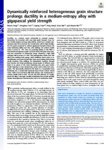
1000
4. Software Tools Speed-up vs RISC
100
Programming of the DREAM architecture is performed at two levels: macro-instructions to be mapped on the datapath are described in single-assignment ANSI-C syntax, and translated to configuration bitstreams by a specific mapping tool [14]. Bitstreams for each macro-instruction are mapped into libraries that are then included in the application code for the embedded Risc core. The application code itself, including references to configuration and computation of macro-instructions is compiled with a retargeted version of the GNU-Gcc compiler. It is possible to simulate/debug the application,and the extension instruction, with a customized release of the GNU-gdb debugger that allows step-by-step evaluation of both C source code and macro-instructions internal description. A Cycle-accurate performance evaluation and code profiling engine is also available, based on SystemC and LISA technology, that can be used as stand alone model or as a library for inclusion in the host SOC systemC simulation environment. All design space exploration is thus performed by the user in a software environment, and performance boosts typical of hardware oriented implementations can be obtained requiring no specific hardware expertise. We believe this to be a very relevant advantage of the introduced architecture.
5
10
Add4x4idct
Sub4x4dct
Sad4x4
Satd4x4
Ofdm_Mapper-1 Ofdm_Mapper-8
Ofdm_Mapper-4 AES-128
1 1
10
100
1000
10000
Interleaving factor
Figure 3. Speed-Up wrt ARM9 processor 1000
Energy efficiency (Mbit/sec/mW)
100
10
1 1
10
100
1000
10000
Add4x4idct
Sub4x4dct
Sad4x4
Satd4x4
Ofdm_Mapper-1 Ofdm_Mapper-8
Ofdm_Mapper-4 AES-128
0,1 Interleaving factor
Figure 4. Energy efficiency (Mbit/sec/mW)
Results and Measurements a mixed custom/semi-custom design flow, while the control and memory addressing sections were designed in HDL and mapped on standard cells libraries. Processor efficiency was measured on a set of computational kernels, oriented toward multimedia and communication applications. In particular, we selected four highly-parallel kernels from the open-source H.264 coding standard [18], an OFDM Constellation Encoder or Mapper [19] (implemented at three levels of unfolding), and well-known symmetric-key cipher AES with 128 key size [20], whose implementa-
The proposed architecture was implemented in CMOS090 nm technology. Most architectural features were silicon proven on preliminary test-chips while a complete prototype of the entire DREAM processor is currently under implementation. Technical Results are described in table 3.2. Top frequency in Worst-Case commercial conditions (125C,0.9V) is 200MHZ, while the device can deliver up to 250MHZ in typical conditions (25C,1V). The reconfigurable datapath was designed with 5
6. Conclusions
100
This paper describes a DSP processor suitable for inclusion as hard IP in state-of-art Systems-on-chip oriented at data-intensive processing. The device, named DREAM, makes use of a medium-grained reconfigurable datapath to process up to 20/40 Gbit/sec on multimedia and telecommunication kernels. Its most relevant features are its small size (18 mm2 ) with respect to other state-of-art RAs, very low time and energy penalty for computation (1.5 us/48 nJ per context), zero configuration overhead and a relevant computation density both both in terms of silicon area and power consumption.
Throughput (GBit/sec)
10
1 1
10
100
1000
10000
0,1 Add4x4idct
Sub4x4dct
Sad4x4
Satd4x4
Ofdm_Mapper-1 Ofdm_Mapper-8
Ofdm_Mapper-4 AES-128
0,01 Interleaving factor
Figure 5. Throughput (Mbit/sec) vs Interleaving factor
References Kernel Add4x4idct Sub4x4dct Sad4x4 Satd4x4 Ofdm-Mapper1 Ofdm-Mapper4 Ofdm-Mapper8 AES-128
GOPS 32.54 48.23 59.28 44.06 4.1 16.1 31.5 4.9
GOPS/mm2 1.8 2.7 3.3 2.45 0.23 0.9 1.8 0.28
GOPS/mW 0.15 0.22 0.33 0.22 0.04 0.10 0.15 0.03
[1] S. Leibson, J. Kim Configurable Processors: a new era in chip design, IEEE Computer, May 2005. [2] ARC International http://www.arc.com [3] W.H.Mangione-Smith et al Seeking solutions in configurable computing, IEEE Computers, Dec 1997 [4] A.DeHon The Density advantage of reconfigurable computing, IEEE Computers, April 2000. [5] I.Bolsen, Challenges and opportunities of FPGA platforms, Proceedings of FPL, 2002 [6] M2000 Embedded FPGA http://www.m2000.fr [7] eSilicon Embedded FPGA http://www.esilicon.com [8] www.elixent.com [9] M. Vorbach, J. Becker, Reconfigurable processor architectures for mobile phones IPDPS, 2003. [10] H. Singh et al. MorphoSys: An Integrated Reconfigurable System for Data-Parallel and Computation-Intensive Applications, IEEE Computers, May 2000. [11] J.M. Arnold S5: architecture and development flow of a software configurable processor, Field-Programmable Technology, 2005 [12] http://www.morpheus-ist.org [13] G. Gao, Y.Wong, Q. Ning A Timed Petri-Net Model for FineGrain Loop Scheduling ACM SIGPLAN , June 1991 [14] C. Mucci, et al. A C-based Algorithm Development Flow for a Reconfigurable Processor Architecture, IEEE International Symposium on System on Chip, 2003. [15] S. Vassiliadis et al., The MOLEN Polymorphic Processor, IEEE Transactions on Computers, November 2004 [16] C.E.Cummings Synthesis and Scripting Techniques for Designing Multi- Asynchronous Clock Designs, SNUG-2001 [17] S.Ciricescu et al., The Reconfigurable Streaming Vector Processor Intl Symposium on Microarchitectures, 2003 [18] VLC media player x264 - a free h264/avc encoder http://developers.videolan.org/x264.html [19] IEEE Standard Air Interface for Fixed Broadband Wireless Access Systems, IEEE 802.16-2004 [20] NIST AES, FIPS PUBS 197. [21] C.Mucci et al., Implementation of the AES/Rjndael algorithm on a dinamically reconfigurable architecture, Proceedings of DATE07
Table 4. Kernel peak performance tion is throughly described in [21]. Performances were evaluated at 200MHZ, and are parametrized with respect to the interleaving factor, intended as the number of data blocks concurrently elaborated. In fact, most multimedia and communication kernels feature thread-level parallelism (i.e. image processing transforms show no correlation across macro-blocks), and interleaving of the elaboration of more than one block allows deeper level of pipelining in computation. The interleaving factor applicable depends also on the available DEB memory budget. All the benchmarks reach a saturation point, where further computation unfolding is made impossible by lack of storage capacity on local memory. Figure 5 describes performance figures, in terms of processed bits per second. Figure 3 describe the boost in term of computation cycles with respect to a standard embedded Risc core. Figure 4 report the throughput normalized with respect to power consumption. Table 5 describes performance for the selected kernels. Considering an ARM926EJ-S processor in the same technology node, according to the vendor Data-Sheets, we would have up to 0.5 GOPS, 0.32 GOPS/mm2 , and 3.5 to 7.1 MOPS/mW. Neglecting overheads due to synchronization, it would thus be necessary to provide up to 60 ordinary processors (thus much higher energy and silicon area) to match the performance delivered by DREAM on computation intensive kernels. 6