Abstract â A conventional digital phase-locked loop (DPLL) is designed using [1] to operate at. 1GHz using 0.18 µm CMOS technology; its lock time is 4.19µs.
A FAST-LOCKING DIGITAL PHASE-LOCKED LOOP By Mahmoud Fawzy Wagdy, Professor Srishti Vaishnava, MSEE Department of Electrical Engineering, California State University, Long Beach, CA, USA Abstract – A conventional digital phase-locked loop (DPLL) is designed using [1] to operate at 1GHz using 0.18 µm CMOS technology; its lock time is 4.19µs. By adding a coarse/fine tuning control unit composed of a digital-to-analog converter (DAC) and a counter as well as switching the currents of the charge pump, a fast-locking DPLL results, with a lock time of 1.02 us, i.e. an improvement by a factor of 4. Simulations for both DPLLs verified the performance improvement due to using a fast-locking technique.
in this research, with a generic technology file “gpdk446”, based on 0.18 µm CMOS technology process.
II. CONVENTIONAL DPLL DESIGN
I. INTRODUCTION The phase-locked loop (PLL) [1-7] constitutes an important “Mixed-Signal” device used in transceivers, communication systems, etc. The PLL recovers clock from digital data signals, recovers the carrier from satellite transmission signals, performs frequency and phase modulation and demodulation and synthesize exact frequencies for receiver tuning. The best-known application of PLLs is clock recovery in communication, frequency synthesis, tracking filter, and phase modulation. Other applications include disk drive control, harmonic compensation, and motor control. The digital PLL (DPLL) is a type of PLLs used to synchronize digital signals. While DPLLs input and outputs are typically digital (square wave), they do have internal functions, which are dependent on analog signals. Thus they are basically known as classical DPLLs. The latest trend in PLLs is the fast-locking PLL, which is of utmost importance to data/clock recovery circuits, spread-spectrum communications, etc. Fast locking is attained via a charge pump circuit, which is divided in to two modules: coarse tuning followed by fine tuning. During coarse tuning, the charge pump current is increased, thus the VCO (voltagecontrolled oscillator) control voltage gets charged at a faster rate, via the loop filter, and hence reducing the lock time. On the other hand, during fine tuning, when DPLL is close to achieving lock [8], the charge pump current is switched back to the original smaller value as used for the conventional DPLL. In this paper, a conventional DPLL is designed, then modified to become a fast-locking DPLL; the lock time is reduced by 4. CADENCE tools are used
Fig. 1. Block Diagram of the Conventional DPLL [1] 1. PFD (Phase-Frequency Detector) [1,9] The block diagram of the PFD is shown in Fig.2.
Fig.2. Phase Frequency Detector (PFD) 2. Charge Pump and Loop Filter The conceptual representation of the charge pump by current sources as well as the connection to the PFD and the loop filter is shown in Fig. 3. The loop filter alone is shown in Fig. 4. Circuit operation is as follows. When the reference input signal (Fref) leads the signal coming from VCO (Fvco), then S1 is closed and S2 is open, thus the UP output of the PFD will cause the charge pump to add charge to the capacitors, thus Vctrl, which is fed to the VCO, is increased. The opposite takes place when Fref lags Fvco. Locking is achieved when both UP and DOWN signals are low, then both the switches S1 and S2 are open and no current flows to the loop filter, thus Vctrl is constant.
Proceedings of the Third International Conference on Information Technology: New Generations (ITNG'06) 0-7695-2497-4/06 $20.00 © 2006
IEEE
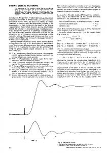
4. Simulation Results A DPLL frequency Synthesizer has been designed for Fref =1GHz [10-14], Vdd = 5V, damping factor=0.802, charge-pump current =150uA, loop filter: C1=60pF, C2=6pF, R=0.8 KOhms, and N=1 (i.e. no divider circuit). Simulation results are shown in Fig.6.
Fig.3. Charge Pump and Loop Filter Connection
Fig. 6. Output Waveform of PLL - Zoomed View to Show Locking Fig. 4. Basic Loop-Filter Circuit 3. VCO (Voltage-Controlled Oscillator) A current-starved VCO is built, which is basically composed of an odd number of transistor stages (greater or equal to 5), is shown in Fig. 5. The VCO oscillation frequency is given by:
f osc
1 N (t1 � t 2)
ID N * Ctot * VDD
(1)
where Ctot is the total load capacitance at the drain of inverters, and t1 and t2 are the charge and discharge times.
It is noted that the PLL is locking at about 4.19µs with Vctrl = 2.70V at locking.
III. FAST-LOCKING DPLL DESIGN 1. Fast-Locking Technique [15,16] For the charge pump, one current source, say CS1, provides smaller amount of fixed current which flows through the loop filter all the time and is given by I fine =150uA. The other current source, say CS2, provides larger amount of current for some initial fixed time interval and is given by I coarse =900uA. During the coarse-tuning period, both current sources (CS1 and CS2) are ON, which means the total current flowing through the loop filter is given by
I total = ( I fine + I coarse )=150uA +900uA=1050uA (2) During the fine-tuning period, CS2 is turned OFF and CS1 is still ON, which means I coarse = 0A and
I fine =150uA. Therefore, the total current flowing through the loop filter during fine-tuning is given by I total = I fine + I coarse =150uA+0=150uA (3) Fig. 5. Current-Starved VCO
Proceedings of the Third International Conference on Information Technology: New Generations (ITNG'06) 0-7695-2497-4/06 $20.00 © 2006
IEEE
2. Architecture of the Fast-Locking DPLL
Fig. 7. Fast-Locking DPLL Schematic* * Design in blue color (Fast-Locking DPLL), design in black color (Conventional DPLL).
Fig. 8. Output Waveform of Charge Pump (with DAC) Showing Coarse and Fine Current
Proceedings of the Third International Conference on Information Technology: New Generations (ITNG'06) 0-7695-2497-4/06 $20.00 © 2006
IEEE
Fig. 9. Plot of Vctrl Voltage of DPLL Showing Zoomed Vcntrl (with Markers) It is noted that the DPLL is locking at about 1GHZ with a lock time of 1.02 µs. 3. Coarse-Fine Control Logic Unit This unit determines the time period for which coarse tuning is performed, i.e., to calculate the time for which the current source (CS2) is ON. During this period large amount of charge pump current flows through the circuit thus charging the loop filter at a faster rate. The coarse-tuning control unit consists of a counter and a one-bit DAC. The counter is used to determine the time for which coarse tuning is performed. It generates a digital pulse, which is ‘high’ for coarse tuning period and is then ‘low’ forever. On the other hand, the onebit DAC is used to convert this digital pulse in to the analog signal (charge pump currentÆ I coarse ). Depending up on the time for which coarse tuning is desired we can select n-bit counter (consisting of n ‘divide-by-2’ circuits in series) and its output will be used to signal DAC to determine I coarse , charge pump current during coarse tuning. The DAC current is set to I coarse = 900uA. Once the n- bit counter has fully counted then it will switch the DAC current to I fine =150uA for fine-tuning. 4. Simulation Results The DPLL charge-pump currents are shown in Fig. 8, and the lock time is shown in Fig. 9.
IV. CONCLUSIONS From the above simulation results of both conventional DPLL and fast-locking DPLL, it was revealed that the lock time of the conventional DPLL=4.19us whereas the lock time of the fastlocking DPLL= 1.02us, i.e. a reduction ratio of 4.10. In other words, the lock time of fast-locking DPLL comes out to be approximately one fourth of the lock time of conventional DPLL (without using fast-lock technique). Hence, the design criterion has been verified by implementing the fast-locking technique.
V. REFERENCES [1] R.Jacob Baker, Harry W. Li, David E. Boyce, “CMOS Circuit Design, Layout, and Simulation.” IEEE Press, 2003. [2] “Synchronization in Digital Communications volume1 Phase-, Frequency-Locked Loops, and Amplitude Control” by Heinrich Meyr, John wiley & Sons Inc., 1990. [3] “Phase Locked Loop Circuit Design” by Dan H. Wolaver, Prentice Hall, Englewood Cliffs. New Jersey 07632. [4] “Phase Locked Loops for Wireless CommunicationsDigital and Analog Implementations” by Donald R. Stephens, Kluwer Academic Publishers, 1998. [5] “Phase Locked Loops- Theory and Applications” by John L. Stenby, Ph.D, Dept. of ECE, Univ. of Alabama, Huntsville, Alabama, CRC Press LLC, 1997. [6] “Phase-Locked Loops- Design, Simulation and Applications”, 4th Edition, by Roland E. Best, McGraw-Hill BC, Inc., 1999.
Proceedings of the Third International Conference on Information Technology: New Generations (ITNG'06) 0-7695-2497-4/06 $20.00 © 2006
IEEE
[7] “Phase-Lock Loop Applications Using the MAX9382”, Dallas Maxium, Application Note 1130, 9th May 2005, < http://pdfserv.maxim-ic.com/en/an/AN1130.pdf>. [8] “PLL Performance, Simulation, and Design” by Dean Banerjee, 2nd Edition, 2001. [9] Kuo-Hsing Cheng, Wei-Bin Yang and Cheng-Ming Ying, “High-speed, Spurious-Free Sequential Phase Frequency Detector and Dual-Modulus Prescalers for RF Frequency Synthesis”, IEEE Symposium on Radio Frequency Integrated Circuits (RFIC), 2003. [10] Neil H. E. Weste, Kamran Eshraghian, “Principles of CMOS VLSI Design”, Addison-Wesley Publishing Company. [11] http://rfdesign.com/mag/radio_debug_pll_frequency/ [12] Tony van Roon, 29th July, 2004, http://www.optics.arizona.edu/Palmer OPTI380B/PDFdocs/PLL%20Tutorial.pdf. [13]http://www.electronics.dit.ie/staff/ypanarin/ Lecture%20Notes/ft221-4/8%20PLL.pdf [14] http://velox.stanford.edu/papers/cky_thesis.pdf [15] L.C.Liu and B.H.Li, “Fast Locking Scheme for PLL Frequency Synthesizer”, Electronics Letters, Vol.40, No. 15, 22nd July, 2004. [16] Asbellatif Bellaouar and Khaled Sharaf, “ Fast Locking/ Self-Tuning VCO Based PLL”, United States Patent No. US 6,566,966, 20th May 2003.
Proceedings of the Third International Conference on Information Technology: New Generations (ITNG'06) 0-7695-2497-4/06 $20.00 © 2006
IEEE