parameters are, silane flow rate (=55sccm), =110mW cm-2,. =20s ...... Louwen, W. G. J. H. M. van Sark, R. E. I. Schropp, W. C.. Turkenburg, and A. P. C. ..... [55] âVerilog-A Language Reference Manual.â [Online]. Available:.
A Framework for Process-to-Module Modeling of a-Si/c-Si Heterojunction Solar Cells to Investigate the Cell-to-Module Efficiency Gap Raghu V. K. Chavali1, Eric C. Johlin2, Jeffery L. Gray1, Tonio Buonassisi2, Muhammad A. Alam1 1
School of Electrical and Computer Engineering, Purdue University, West Lafayette, IN, USA
2
Department of Mechanical Engineering, Massachusetts Institute of Technology, Cambridge, MA, USA
Abstract — The cell-to-module efficiency gap observed in a-Si/cSi heterojunction solar cells is a key challenge the broad adoption of this technology. To systematically address this issue, we describe an end-to-end modeling framework to explore the implications of process and device variations at the module level. First, a process model is developed to connect the a-Si deposition parameters to the material properties. Next, a physics based device model is presented; the model uses the thermionic emission/diffusion theory to capture the essential features of photo-current and diode injection current. Using the process and device models, the effects of process conditions on cell performance are explored. Finally, the performance of the module, as a function of device and process parameters, is explored to establish the cell-to-module efficiency gap. The insights developed through this process-to-module modeling framework may help close the cell-to-module efficiency gap of this commercially promising technology. Index Terms — amorphous semiconductors, current-voltage characteristics, heterojunctions, process control, silicon, modeling and simulation
I. INTRODUCTION a-Si/c-Si heterojunction solar cell (SHJ) is a promising THE technology [1], [2], due to its high efficiencies (with standard cell record efficiency of 25.1% [3] and IBC cell of >25% [4], [5]), and power output that is relatively insensitive to the operating temperature [6], [7]. Several groups have demonstrated lab cell efficiencies exceeding 22% [8]. Further, large scale commercialization of the technology appears promising, because rigorous cost calculations [9] project a module cost of ~$0.5/Wp (comparable to c-Si); indeed, the price may drop further to ~$0.3/Wp with design improvements [10]. In addition, improvements, such as, the use of new carrier collectors [11], [12], TCO materials [13], c-Si surface engineering [14], bifacial configuration [15], [16], interdigitated back contact (IBC) configuration [4], [5], [17], local heterojunction contacts[18], silicon heterojunction tandems [19]–[22] and bifacial-tandem configuration [23] have all been proposed towards this goal. These improvements need This paper is based upon work supported in part under the US-India Partnership to Advance Clean Energy-Research (PACE-R) for the Solar Energy Research Institute for India and the United States (SERIIUS), funded jointly by the U.S. Department of Energy (Office of Science, Office of Basic Energy Sciences, and Energy Efficiency and Renewable Energy, So- lar Energy Technology Program, under Subcontract DE-AC36-08GO28308 to the National Renewable Energy Laboratory, Golden, Colorado) and the Government of India, through the Department of Science and Technology under Subcontract IUSSTF/JCERDCSERIIUS/2012 dated 22nd Nov. 2012. Jeffery L. Gray and Muhammad A. Alam were supported by the Department of Energy through the Bay Area Photovoltaic Consortium under Award Number DE-EE0004946. Additional resources are provided by the NSF and SRC through the NCN-NEEDS program (1227020-EEC).
to be translated to the module performance for the large scale commercialization of this technology. Although high efficiencies are demonstrated at the cell level, the sensitivity to process variations is a persistent concern for the module efficiency, and hence, for the prospect of large-scale deployment [8]. This adds to the other variability concerns related to module performance: namely, losses due to series resistance and dead area. There are a large number of device related parameters, such as, c-Si wafer quality, a-Si film properties, TCO properties, contacts etc, which can affect the ultimate performance of cell and the module. The connection between the key process parameters, the heterojunction (HJ) device characteristics and the module parameters can help establish the ultimate performance limit and the long-term commercial viability of a PV technology. It requires careful and self-consistent modeling and optimization at the process, device, and module levels to reduce the cell-to-module efficiency gap (Δ). Here, we define the idealized cell-to-module efficiency gap (Δ) as the efficiency loss between an idealized cell efficiency (that can be achieved for optimized process conditions, excluding the resistance and shunt losses) and the ultimate module efficiency (including the dead-area loss, etc.) ready for deployment (see Fig. A4 in appendix, for cell and module efficiencies for a range of technologies). Note that Δ is the absolute efficiency difference. The optimization at each level (process, device, module) required to reduce Δ solely based on trial-and-error experiments, or by first principle numerical simulation can be impractical. Instead, one may adopt the multiscale end-to-end modeling methodology previously demonstrated for OPVs [24] and CdTe solar cells [25]. The approach must be adapted for SHJ technology so that one can describe the details of process conditions, capture the essence of HJ-limited carrier transport [26], and simulate the effects of module configuration, fundamentally different than those used for thin-film PV (TFPV). Ideally, a compact modeling approach which captures the essential features of the process conditions, HJ transport and the module can be an efficient way to study the connection between the process, device and module parameters and can help unravel the origin of Δ. With several companies entering the production phase of this technology, a systematic approach to analyze the contributions to Δ can be crucial to improve the module efficiencies to > 20%. In this paper, we consider the impact of a subset of process parameters (specifically, those that affect a-Si film quality) on the ultimate cell-to-module efficiency gap of the SHJ technology. Using these process parameters, our goals are to
This manuscript is the accepted copy. Please find the published version (© IEEE) through IEEE Xplore. Link: http://dx.doi.org/10.1109/JPHOTOV.2016.2557060
characteristics (𝐽𝐷𝑖𝑜𝑑𝑒 , 𝐽𝑃ℎ𝑜 ) and the module parameters (𝜂, Δ) are studied. First, we will present a semi-empirical process model along with its influence on the a-Si film properties. Next, we will develop a physics based HJ device model to study the influence of process parameters on the device performance. Finally, we will describe the module model and study the influence of process/shunt parameters, resistance, dead area loss and cell sorting on the cell-to-module efficiency gap of SHJ technology. This study may also serve as an illustrative example for process-to-module optimization flow for other PV technologies. II. AMORPHOUS SILICON PROCESS MODEL
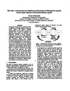
Fig. 1. (a) The end-to-end modeling framework for a-Si/c-Si heterojunction cells is shown. It shows the process variations in deposition pressure (𝑃𝑝 ), temperature (𝑇𝑝 ), plasma power density (𝑊), [𝐵2 𝐻6 ]/[𝑆𝑖𝐻4 ] (𝑅𝑔 ), deposition time (𝑡𝑑𝑒𝑝 ) during the deposition of the a-Si film lead to variation in the bandgap (𝐸𝐺 ), the average Fermi-level in doped the a-Si emitter (〈𝐸𝑓𝑝 − 𝐸𝑉 〉), film thickness of i-layer (𝑡𝑖 ) and p-layer (𝑡𝑝 ), which eventually dictate the variation in diode (𝐽𝐷𝑖𝑜𝑑𝑒 ) and photocurrent (𝐽𝑃ℎ𝑜 ) characteristics of individual cells, and finally the module efficiency (𝜂) and cell-to-module efficiency gap (Δ). (b) Schematic of energy band diagram under equilibrium indicating the key process dependent device parameters considered in this study. demonstrate (i) the viability of an end-to-end modeling if the
process parameters are specified, and (ii) even if the other factors are presumed perfect, a significant cell-to- module gap persists, attributed to a-Si:H deposition alone. The end-to-end modeling approach can be beneficial for rapid technology prototyping and quality control. We focus on the specific technology and subset of process parameter purely as an illustrative example. Our choice does not imply that cell-tomodule gap or process windows are fundamentally different from other technologies. The variation in a-Si film properties can be due to the process variations in deposition pressure (𝑃𝑝 ), temperature (𝑇𝑝 ), plasma power density (𝑊), [𝐵2 𝐻6 ]/[𝑆𝑖𝐻4 ] (𝑅𝑔 ), deposition time (𝑡𝑑𝑒𝑝 ) during the deposition of the a-Si film (see Fig. 1(a)). This can lead to variation in the bandgap (𝐸𝐺 ), the average Fermi-level in doped the a-Si emitter (〈𝐸𝑓𝑝 − 𝐸𝑉 〉), the film thickness of ilayer (𝑡𝑖 ) and p-layer (𝑡𝑝 ), and the attenuation coefficient (𝑘) (see Fig. 1(b)), which eventually dictate the variation in diode (𝐽𝐷𝑖𝑜𝑑𝑒 ) and photocurrent (𝐽𝑃ℎ𝑜 ) characteristics of individual cells, and finally the module efficiency (𝜂) [27]. This cell-tocell variation can be one of the main sources of cell-to-module efficiency gap (Δ). Precisely, in this work, the connection between the key a-Si deposition process parameters (𝑃𝑝 , 𝑇𝑝 , 𝑊, 𝑅𝑔 , 𝑡𝑑𝑒𝑝 ), the front a-Si film parameters (𝐸𝐺 , 𝐸𝑓𝑝 , 𝑡𝑖 , 𝑡𝑝 , 𝑘), the HJ device
The deposition of a-Si on the c-Si wafer can introduce significant process variations which can ultimately impact the cell-to-module efficiency gap. For example, a small change in 𝑇𝑝 or 𝑃𝑝 may significantly affect the a-Si/c-Si band-offset (Δ𝐸𝑉 ) (see Fig. 1(b)) which in-turn reduces collection efficiency and the fill-factor (𝐹𝐹). Both the front and back a-Si layers can impact the performance of the cell, however, in good quality cells, the impact of front a-Si layer is dominant. Here, the a-Si process model which can predict the film properties (𝐸𝐺 , 𝐸𝑓𝑝 , 𝑡𝑖 , 𝑡𝑝 , 𝑘) based on the a-Si deposition conditions (𝑃𝑝 , 𝑇𝑝 , 𝑊, 𝑅𝑔 , 𝑡𝑑𝑒𝑝 ) is presented. A. Process Compact Model The mechanism of a-Si film growth and the evolution of microstructure during PECVD deposition are reasonably well understood [28]. There is experimental evidence that the film properties depend a fundamental plasma parameter known as ‘silane depletion fraction’ (SDF), which measures the reduction of silane partial pressure due to dissociation of plasma [29]. The SDF is in turn controlled by the deposition conditions, such as, 𝑃𝑝 ,𝑇𝑝 , 𝑊 of the plasma, as discussed in [30]. The basic physics of a-Si growth has been proven to be accurate even for a-Si deposition during the fabrication of SHJ solar cells [31]. It is important to note that the exact dependencies of process parameters on the film properties can differ significantly from one deposition tool to another, hence, the intent here is not to provide an exact model of all PECVD deposition of a-Si (as this is impossible due to the large variety of deposition tools), but rather to explore the complex influences of different parameters in the a-Si deposition on the module efficiencies. One has to calibrate this process model to the exact PECVD deposition tool before proceeding to the device and module analysis presented in this work. Here, we utilize the large amount previous work [32]–[37] into developing the empirical relationships for the process model. For example, we know empirically that the band gap depends strongly on the ion momentum [38]. Since the ion momentum depends on pressure and power, we can define a model that correlates bandgap to these variables. Temperature is expressed a secondary influence, which is then incorporated as a modification of the base band gap calculation [33]–[35]. Doping does not have a strong influence on band gap [39], so it is neglected for bandgap calculation. This
This manuscript is the accepted copy. Please find the published version (© IEEE) through IEEE Xplore. Link: http://dx.doi.org/10.1109/JPHOTOV.2016.2557060
Fig. 2. (a) The compact model fit for the measured intrinsic a-Si bandgaps (𝐸𝐺𝑖 ). The other process conditions are held constant at 𝑇𝑃 =200 °C, 𝑊 =164 mW cm-2, pure silane (𝑅𝑔 =0). (b) The compact model fit for the measured p-doped a-Si Fermi level (𝐸𝑝𝑓 − 𝐸𝑣 ) [59]. The other process conditions are held constant at 𝑇𝑃 =27 °C, 𝑊 =164 mW cm-2, 𝑃𝑝 = 760𝑚𝑇𝑜𝑟𝑟. The bandgap is not assumed to vary with 𝑅𝑔 .
systematic/hierarchical approach allows us to compute film properties over a large deposition space without requiring a prohibitive number of test depositions and will help manufacturers attempting to optimize their process flow. For a specific PECVD system, the accuracy can be improved by increasing the number of test samples. The modeling of the a-Si material deposition processparameter relationships begins with the establishment of a baseline process condition. Here we use a fixed 𝑇𝑃 =200 °C, and 𝑊 =164 mW cm-2, with pure silane ([𝐵2 𝐻6 ]/[𝑆𝑖𝐻4 ]=𝑅𝑔 =0). Experimental films at this condition for a variety of pressures ranging from 200 to 1000 mTorr were deposited, with material properties such as 𝐸𝐺 (see Fig. 2(a)), stress, thickness and density measured. Details of the process have been reported previously [38]. As discussed in [38], [40], with the increase in 𝑃𝑝 the Hydrogen content in the a-Si film increases, which in turn increases the 𝐸𝐺 of the a-Si film as shown in Fig. 2(a). Additional films with varying 𝑊 were deposited, allowing a two-dimensional interpolation between the power-pressure space to be made for the material properties. Pressure was chosen as the most finely-measured parameter, as it was previously determined to have the largest influence on film parameters, over a reasonable deposition range. The influences of deposition temperature was determined both experimentally for select conditions, as well as modeled from relationships reported in the literature [32]. Then, they were extrapolated as deviations on the base conditions in order to obtain predictions of 𝐸𝐺 [33]–[35], 𝑘 (measured at 𝜆 =633nm), 𝑡𝑝 and 𝑡𝑖 [37]. Similarly, dopant gas incorporation ([𝐵2 𝐻6 ]/[𝑆𝑖𝐻4 ]=𝑅𝑔 ) was modelled using data from literature
[36] to set the Fermi level in p-doped a-Si layer 𝐸𝑓𝑝 (see Fig. 2(b)). For example, for a simulated deposition at 𝑃𝑝 =800 mTorr, 𝑇𝑝 =150 °C and 𝑅𝑔 =0.01, the standard deposition properties at 𝑇𝑝 =200 °C with pure silane are first calculated for the 𝑃𝑝 =800 mTorr pressure, and then shifted with the predicted modifications for both 𝑇𝑝 =150 °C, and 𝑅𝑔 =0.01. In addition to the process parameters used in developing the model, hydrogen dilution can be an important factor in controlling the bandgap of the film. In general, hydrogen incorporation is a complex phenomenon, as hydrogen dilution may increase or decrease the hydrogen content of the produced films, depending on the deposition regime of the PECVD plasma. Therefore, in this initial study, we simplified the model by not treating hydrogen dilution as an explicit parameter, even though the hydrogen contents do vary substantially (from ~1.5 × 10²¹ to ~1.5 × 10²² 𝑐𝑚−3 ) as the deposition pressure varies (from 100mTorr to 2000mTorr), see [38] for additional details. Although the parameterized model for film properties depends on the details of the reactor/plasma, as well as the process variables considered explicitly, our approach of parameterization of the growth kinetics in terms of dominant process variables (and using the information within an end-toend modeling framework) should be broadly useful; indeed, the model can be generalized to include additional parameters (e.g. hydrogen dilution) if sufficient empirical data is available. B. Influence of Process Parameters Here, we present the process condition dependence of key aSi film properties, such as, 𝐸𝐺 , 𝐸𝑓𝑝 − 𝐸𝑉 and 𝑡𝑖 , 𝑘. As an illustration, we present these parameter variation as a function of the deposition pressure (𝑃𝑝 ) for various temperatures (𝑇𝑝 =150°C, 200°C, 250°C), see Fig. 3 for a p-doped a-Si layer. The other input parameters, silane flow rate (𝐹=55sccm), 𝑊=110mW cm-2, deposition time (𝑡𝑑𝑒𝑝 =20s), dopant gas ratio (𝑅𝑔 =0.01). As mentioned in section II A, the dopant gas ratio only effects the Fermi-level position (𝐸𝑓𝑝 − 𝐸𝑉 ). Hence, 𝐸𝐺 and 𝑘 are assumed to be same as that of an intrinsic a-Si layer deposited at the above conditions with 𝑅𝑔 = 0. While 𝑇𝑝 and 𝑃𝑝 are the only process parameters shown here, this general procedure would allow one to calculate the influence of any combination of process parameters (𝑃𝑝 , 𝑇𝑝 , 𝑊, 𝑅𝑔 , 𝑡𝑑𝑒𝑝 ) of the simulated material. III. HETEROJUNCTION DEVICE MODEL In this section, we analyze the influence of process parameters on the efficiency of the SHJ cell. As mentioned in section I, the properties of the a-Si/c-Si HJ cause several nonideal effects even in good quality cells, thereby degrading their efficiencies. The non-ideal features in the experimental IV characteristics, such as, the failure of superposition between the light and the dark I-V, the injection limited transport in diode current (𝐽𝐷𝑖𝑜𝑑𝑒 ) [26], the occurrence of S-type curve in photocurrent (𝐽𝑃ℎ𝑜 ) [26], [41] are all attributed to the presence of large Δ𝐸𝑉 and low emitter doping. These non-ideal features are
This manuscript is the accepted copy. Please find the published version (© IEEE) through IEEE Xplore. Link: http://dx.doi.org/10.1109/JPHOTOV.2016.2557060
emission theory [45]. The mathematical formulation is discussed in appendices A and B. Here we present the final expression for 𝐽𝑃ℎ𝑜 , given by 𝑠𝐷−1 + 𝑠𝑏−1 𝐽𝑝ℎ𝑜 ≅ −𝑞𝑁𝑐𝑆𝑖 ( −1 ), (1) −1 𝑠𝑓𝑙 + 𝑠−1 𝐷 + 𝑠𝑏 where, 𝑁𝑐𝑆𝑖 is the effective rate of carriers generated per unit area inside the quasi-neutral c-Si layer, dependent on the a-Si (𝑡𝑖 , 𝑡𝑝 ) and c-Si quasi-neutral region and the corresponding 𝑘 values (see Appendix B); 𝑠𝑏 is the surface recombination velocity at the back interface; and 𝑠𝐷 is the diffusion velocity in c-Si quasi-neutral region given by 𝑠𝐷 = 𝐷ℎ (
1
𝑊𝑐
Fig. 3. (a) 𝐸𝐺 , (b) 𝐸𝑓𝑝 − 𝐸𝑉 , (c) 𝑘, on left axis and 𝑡𝑝 , on right axis dependence on 𝑃𝑃 for three different 𝑇𝑝 (= 150° 𝐶, 200° 𝐶, 250° 𝐶) are shown. The arrow indicates the increase of 𝑇𝑝 . The other input parameters are, silane flow rate (=55sccm), 𝑊=110mW cm-2, 𝑡𝑑𝑒𝑝 =20s, 𝑅𝑔 =0.01.
well understood and modeled using numerical simulations (see Fig. 4(a-c)) [26], [41] and semi-empirical modeling [42], [43]. However, these models cannot be scaled from the process level to the module level due to either their limited physical nature or inherent computational complexity. Hence, we need to develop a physics-based compact model to capture the distinctive features of I-V characteristics (𝐽𝐷𝑖𝑜𝑑𝑒 , 𝐽𝑃ℎ𝑜 ) and relate it to the a-Si and HJ properties such as, Δ𝐸𝑉 , 𝐸𝑓𝑝 , 𝑡𝑖 , 𝑘, 𝑁𝐼𝑇 . Using this compact model, along with the process model described in section II, we can explore the process sensitivity of cell-level performance parameters. A. Device Compact Model The standard two-diode model that is typically used to model a standard c-Si solar cell cannot be translated directly to SHJ cell due to the inherent complexity of the carrier transport in SHJ cells. Hence, to develop the device model, we need to model the two current components 𝐽𝑃ℎ𝑜 and 𝐽𝐷𝑖𝑜𝑑𝑒 separately. Here, 𝐽𝑃ℎ𝑜 is the current component due to the photo-generated carriers and 𝐽𝐷𝑖𝑜𝑑𝑒 is the current component from the contact injected carriers (see [44] for details). The total current is given by 𝐽𝑡𝑜𝑡 = 𝐽𝑃ℎ𝑜 + 𝐽𝐷𝑖𝑜𝑑𝑒 . Ideally, both 𝐽𝑃ℎ𝑜 and 𝐽𝐷𝑖𝑜𝑑𝑒 are dependent on the generation rate (𝐺) and applied bias (𝑉) as described in [26], [44]. However, for the compact model we focus on the major contributions for SHJ cell, which are 𝐽𝑃ℎ𝑜 (𝐺, 𝑉) and 𝐽𝐷𝑖𝑜𝑑𝑒 (𝑉). To capture the above mentioned features, 𝐽𝑃ℎ𝑜 , 𝐽𝐷𝑖𝑜𝑑𝑒 are modeled using diffusion-thermionic
+
1 𝐿𝑝
) , where
𝐷ℎ is the diffusion coefficient for holes and 𝑊𝑐 is the thickness of the quasi-neutral region, 𝐿𝑝 is the hole diffusion length in cSi. The 𝑠𝑓𝑙 is the emission-diffusion velocity in a-Si under light given by 𝑠𝑓𝑙 = 𝑠𝑜 𝑒 −(Δ𝐸𝑉 −𝜙𝑁𝑙 )⁄𝑘𝑏 𝑇 , and 𝜙𝑁𝑙 = 𝜙𝑁𝑙 (𝑉 = 0) − 𝛽𝑙 𝑉, 𝛽𝑙 is the ratio of potential developed in c-Si region to the applied voltage (𝑉) under illumination and 𝜙𝑁𝑙 is the electrostatic potential in the c-Si depletion region under illumination (subscript ‘𝑙’ stands for light) (see 𝜙𝑁 in Fig. 1(b)). Intuitively, (1) indicates that the smallest of 𝑠𝑓𝑙 , 𝑠𝐷 , 𝑠𝑏 is the rate limiting factor and dictates the magnitude of 𝐽𝑃ℎ𝑜 . Similarly, the minority carrier current,𝐽𝐷𝑖𝑜𝑑𝑒 , is given by 2 𝑛𝑖𝑐 1 𝐽𝐷𝑖𝑜𝑑𝑒 = 𝑞 ( −1 ) (𝑒 𝑞𝑉/𝑘𝐵𝑇 − 1). (2) 𝑁𝐷 𝑠𝑓𝑑 + 𝑠𝐷−1 Here, 𝑛𝑖𝑐 is the intrinsic carrier concentration in the absorber layer, 𝑠𝑓𝑑 = 𝑠𝑜 𝑒 −(Δ𝐸𝑉 −𝜙𝑁𝑑 )⁄𝑘𝑏𝑇 , where 𝜙𝑁𝑑 = 𝜙𝑁𝑑 (𝑉 = 0) − 𝛽𝑑 𝑉, 𝛽𝑑 is the ratio of potential developed in c-Si depletion region to the applied voltage (𝑉) under dark, 𝜙𝑁𝑑 is the electrostatic potential in the c-Si depletion region under dark (subscript ‘𝑑’ stands for dark). Intuitively, (2) indicates that the smaller of the two velocities (𝑠𝑓𝑑 , 𝑠𝐷 ) defines the rate limiting factor and dictates the magnitude of 𝐽𝐷𝑖𝑜𝑑𝑒 . Further, an external series resistance 𝑅𝑠𝑒𝑟𝑖𝑒𝑠 , is also included as an extrinsic parameter in the device compact model (see Fig. 6 (c) for the device compact model). In addition, the shunt conductance (𝐺𝑆ℎ𝑢𝑛𝑡 ) is modeled as an extrinsic parameter using the following relation [46], [47] 𝐽𝑆ℎ𝑢𝑛𝑡 = 𝐺1𝑆ℎ 𝑉 + 𝐺2𝑆ℎ 𝑉 2 ,
(4)
where,𝐺1𝑆ℎ accounts for ohmic transport and 𝐺2𝑆ℎ accounts for the space-charge limited transport. A close match between the experimental (obtained from [48]) and the compact model is presented in the Fig. 4 for two samples with low and high FFs. The device parameters extracted by fitting the experimental data to the compact model are presented in the appendix Table A2. For the low FF device, the compact model accurately captures the effect of current saturation of 𝐽𝐷𝑖𝑜𝑑𝑒 at high voltages, which is due to injectionlimited transport in HJ (see Fig. 4(a)) [26]. Further, it also accounts for the S-type curve of 𝐽𝑃ℎ𝑜 below 𝑉𝑂𝐶 , which is due to the HJ barrier for minority carrier collection (see Fig. 4(c)) [26]. As expected, these correlated non-idealities in dark and light I-V are not present in the high FF cell, see Fig. 4(b, d))[26]. This indicates that the compact model can capture the essential features of dark and light I-V accurately. Finally, we
This manuscript is the accepted copy. Please find the published version (© IEEE) through IEEE Xplore. Link: http://dx.doi.org/10.1109/JPHOTOV.2016.2557060
Fig. 4. The 𝐽𝐷𝑖𝑜𝑑𝑒 obtained from experiments (□) [48] and compact model (−), indicating the current saturation (marked in green) for (a) voltages > 0.5𝑉 for low quality sample, and (b) > 0.7𝑉 for high quality samples. The corresponding 𝐽𝑃ℎ𝑜 also indicates the expected shift in rollover voltage (marked in green) for (c) low and (d) high quality samples. [26]
benchmark the compact model against numerical simulations [44], [49], these results are presented in appendix C. B. Influence of a-Si Process Parameters As mentioned earlier, the exact process dependencies on the cell performance can vary significantly from one fabrication flow to another. Here, we illustrate the usefulness of the endto-end modeling framework in process optimization studies using the process and device model presented earlier. As described in section III A, the four key a-Si film/HJ parameters that significantly affect the performance of the SHJ cell are Δ𝐸𝑉 , 𝑁𝑐𝑆𝑖 , 𝐸𝑓𝑝 and 𝑁𝐼𝑇 . On the other hand, the a-Si process model discussed in section II A, provides the following five aSi film properties as its output (𝐸𝐺 , 𝐸𝑓𝑝 , 𝑡𝑖 , 𝑡𝑝 ,𝑘). To map these five a-Si film parameters to the four device parameters, we first note that 𝐸𝑓𝑝 is obtained directly. The other three parameters ( Δ𝐸𝑉 , 𝑁𝑐𝑆𝑖 and 𝑁𝐼𝑇 ) are obtained as follows. Using the 𝐸𝐺 , we can estimate the Δ𝐸𝑉 = (𝜒 + 𝐸𝐺 ) − (𝜒𝑐 − 𝐸𝐺𝑐 ), where 𝜒 is electron affinity of intrinsic a-Si, 𝜒𝑐 and 𝐸𝐺𝑐 are the electron affinity and bandgap of c-Si, and are obtained from literature [27]. Note that the conduction band offset (Δ𝐸𝐶 ) is determined by 𝜒 and 𝜒𝑐 and it does not play a significant role in minority carrier (hole) collection in in the operating bias range. Using 𝑡𝑖 , 𝑡𝑝 and 𝑘 the effective generation rate in c-Si absorber (𝑁𝑐𝑆𝑖 ) can be calculated using Beer-Lambert’s law (see Appendix B for details). The effect of 𝑁𝐼𝑇 is account through the interface recombination velocity 𝑠𝑏 (see eq. (1), (2)) in the device model. In addition, the collection properties of the a-Si layer are modeled through the a-Si emission-diffusion velocity 𝑠𝑓 (see Appendix A and B for details). Based on the process dependence of Δ𝐸𝑉 , 𝑁𝑐𝑆𝑖 , 𝐸𝑓𝑝 described in Fig. 3, we explore the corresponding process pressure dependence on the cell performance parameters, shown in Fig. 5(a-d). The deposition temperature (𝑇𝑝 ) is set to 200°C. The
other process conditions are set to their baseline case as mentioned in Fig. 3. The effect of interface recombination is studied by varying 𝑠𝑏 (values of 1cm/s, 10 cm/s and 100cm/s, arrows in Fig. 5 (a, c, d) indicate increasing 𝑠𝑏 ). The value of 𝑠0 used in the calculation of 𝑠𝑓 is assumed to 105 𝑐𝑚/𝑠 (see Appendix A and B). The 𝐹𝐹 starts to drop-off rapidly for 400 𝑚𝑇𝑜𝑟𝑟 < 𝑃𝑃 < 800 𝑚𝑇𝑜𝑟𝑟. This is due to increase in Δ𝐸𝑉 , which effects 𝐽𝑃ℎ𝑜 through the S-type curve. In addition, at a given 𝑃𝑝 , the 𝐹𝐹 improves with smaller 𝑠𝑏 . 𝐽𝑠𝑐 is affected by the film properties such as 𝑡𝑖 , 𝑡𝑝 , 𝑘 and improves for smaller values of 𝑡𝑖 , 𝑡𝑝 , 𝑘 [50]. Since, 𝑡𝑖 (𝑡𝑝 ) and 𝑘 have oppose trends with 𝑃𝑝 (see Fig. 3(c)), the resulting 𝐽𝑠𝑐 is observed to have very small variation with 𝑃𝑝 . Further, it is observed that 𝑠𝑏 has little impact on 𝐽𝑠𝑐 . As expected, 𝑉𝑜𝑐 follows 𝐸𝑓𝑝 − 𝐸𝑉 as this quantity controls 𝑠𝑓 and thus 𝐽𝐷𝑖𝑜𝑑𝑒 (see eq. 2). Also, 𝑉𝑜𝑐 is observed to drop with higher 𝑠𝑏 due to higher recombination losses. Finally, 𝜂 shows a ‘V’ shape trend with 𝑃𝑝 and observed to be fairly constant for very small values of 𝑠𝑏 . Further, we can also perform sensitivity studies on each process parameter (𝑃𝑝 , 𝑇𝑝 , 𝑊, 𝑅𝑔 , 𝑡𝑑𝑒𝑝 ) on the cell efficiency, 𝜂. Fig. 5 (e) shows the tornedo plot for sensitivity analysis of process parameters: 𝑇𝑝 =200°C, 𝑃𝑝 =900 mTorr, 𝑊=110mW cm2 , 𝑡𝑑𝑒𝑝𝑖 =20s, 𝑅𝑔 =0.02, while 𝑡𝑑𝑒𝑝𝑝 is fixed at 25s. A variation of 10% is considered for this sensitivity analysis. Hence, for the process model used here, we observe from Fig. 5(e) that 𝑊 and 𝑇𝑝 have the greatest sensitivity towards the cell 𝜂, while the rest of the process parameters have less impact. C. Discussion on additional process parameters There are several other factors that can cause significant variation in the cell performance such as c-Si wafer quality, choice of TCO etc., which weren’t included in the process-tomodule modeling framework discussed in this paper. Here we will discuss pathways to introduce these effects into the device modeling framework. i.. TCO work-function The effect of TCO can be effectively captured in 𝑠𝑓𝑙/𝑑 = 𝑠0 𝑒 −(𝜙𝑁𝑙/𝑑−Δ𝐸𝑉 )/𝑘𝑇 as follows: 1. Transport: The recombination velocity at the contact can depend on the type of TCO, thus, effects and can be calibrated for specific TCO to obtain corresponding 𝑠0 . 2. Electrostatics: The work-function of TCO can be captured by modifying the value of 𝜙𝑁 . The exact relationship can depend on several factors such as, doping in emitter, concentration of inversion charge at the a-Si/c-Si interface (which can introduce screening effect in c-Si bulk). Hence, this parameter requires calibration to experiments. One can use the C-V analysis described in [27] to estimate 𝜙𝑁 for a series of devices with different TCO/contact work-functions. ii. c-Si wafer quality The properties of c-Si wafer can be captured through the mobility (𝜇) and lifetime (𝜏) properties. If this information is available from the feedstock, it is possible to incorporate these
This manuscript is the accepted copy. Please find the published version (© IEEE) through IEEE Xplore. Link: http://dx.doi.org/10.1109/JPHOTOV.2016.2557060
recombination at the front interface can be captured into the terms 𝑠𝑓𝑙/𝑑 . The recombination at the front interface 𝑠𝑓𝐼𝑇 is subtracted from the prefactor 𝑠𝑜 present in 𝑠𝑓𝑙/𝑑 , to exclusively account for the carriers that get collected (under illumination) at the front contact. IV. MODULE PERFORMANCE To improve the module performance, it is crucial to understand the impact of fabrication parameters on the module efficiency. Here, we will study the effect of process and shunt variation on the module performance. In order to study these effects, we will use a multi-stage modeling approach to model the module performance using the device compact model described in section III. A. Module Compact Model
Fig. 5. 𝑃𝑃 dependence on (a) 𝐹𝐹 (b) 𝐽𝑆𝐶 (c) 𝑉𝑂𝐶 (d) 𝜂 of the cell for different values of interface recombination velocity (𝑠𝑏 =1cm/s, 10cm/s, 100cm/s). The arrow indicates the direction of increasing 𝑠𝑏 . All other process parameters are assumed to be at the baseline given in Fig. 3 and 𝑇𝑝 = 200° 𝐶. (e) The sensitivity plot of process parameters on cell 𝜂. The baseline deposition pressure is 𝑃𝑝 = 900 𝑚𝑇𝑜𝑟𝑟. The red (blue) color indicates the effect on cell 𝜂 for 10% decrease (increase) in corresponding process variable.
effects into the c-Si diffusion velocity 𝑠𝐷 = 𝐷ℎ (
1
𝑊𝑐
𝐷ℎ 𝑊𝑐
+√
𝑘𝑇𝜇 𝑞𝜏
+
1 𝐿𝑝
)=
.
iii. Interface defects at the front a-Si/c-Si interface The connection between the i-layer deposition conditions and the effective lifetime (𝜏𝑒𝑓𝑓 ) measured using the quasi-steady state photoconductive decay (QSSPC) [51] can be used to estimate the interface recombination, for example, ref. [52]. Using this effective lifetime, one can estimate the interface 1 recombination velocity at the front and back interface as = 1 𝜏
+
𝑠𝑓𝐼𝑇 𝑊𝑐
The multi-stage modeling approach of the module compact model is presented in Fig. 6. At the top stage, 8 x 11 cells (of size 131.5 mm x 131.5 mm each, ref. datasheet [53]) are connected in series to form a full module. In the second stage, each cell is modeled with 70 x 15 sub-cells. The three bus-bars on each cell are located at 3rd, 8th and 13th columns. To model the state-of-the-art modules we assume the low yet practical values of resistances of the grid layers. The sub-cells are connected to each other and to the bus-bar through resistor elements to model the metal finger (with cross-section of 120 𝜇𝑚 x 65𝜇𝑚) and bus-bar (with cross-section of 1500 𝜇𝑚 x 150 𝜇𝑚) resistances, with metal resistivity of 2 𝜇Ω. 𝑐𝑚 (Silver resistivity is 1.6 𝜇Ω. 𝑐𝑚). In the last stage, each sub-cell is modeled using a compact model shown in Fig. 6 (c). The TCO sheet resistance (50Ω/□) is modeled as 𝑅𝑆𝑒𝑟𝑖𝑒𝑠 in the device compact model. The intrinsic components (𝐽𝑃ℎ𝑜 and 𝐽𝐷𝑖𝑜𝑑𝑒 ) are obtained from device model as discussed in section III A. The grid shadow is accounted through the 𝑁𝑐𝑆𝑖 parameter in eq. (1). The dead area to be 7% [53] of the overall module area. The module model is simulated using HSpiceTM simulation tool [54]. The device model for 𝐽𝑃ℎ𝑜 and 𝐽𝐷𝑖𝑜𝑑𝑒 is implemented using Verilog-ATM toolbox [55]. B. Influence of Process/Shunt Variations
𝜏𝑒𝑓𝑓
+
𝑠𝑏 𝑊𝑐
, where 𝜏 is the lifetime in c-Si wafer, interface
recombination velocity at the front interface, 𝑠𝑏 is the recombination at the back interface and 𝑊𝑐 is the thickness of c-Si quasi-neutral region. The terms for bulk and back interface recombination are already included in the device model as 𝑠𝐷 = 𝐷ℎ (
1
𝑊𝑐
+
1 𝐿𝑝
)=
𝐷ℎ 𝑊𝑐
𝑘𝑇𝜇
+ √ 𝑞𝜏 and 𝑠𝑏 respectively, where 𝐷ℎ is
the diffusion coefficient for holes, 𝐿𝑝 is the hole diffusion length in c-Si, 𝜇 is c-Si hole mobility. The surface
Fig. 6. The schematic of (a) series connected cells in module, (b) sub-cells within a cell connected with resistor elements to model the bus-bar (𝑅𝑏𝑢𝑠 ) and the finger (𝑅𝑓𝑖𝑛 ) resistances (c) sub-cells circuit within a cell with the intrinsic and extrinsic components.
This manuscript is the accepted copy. Please find the published version (© IEEE) through IEEE Xplore. Link: http://dx.doi.org/10.1109/JPHOTOV.2016.2557060
This multi-stage modeling of a module provides a unique opportunity to analyze both the microscopic features, such as the shunt variations within a cell, and macroscopic features, such as the cell-to-cell process parameter variations within a module. Here, we will study both these microscopic and macroscopic variations with the help of the process, device and module models developed in this work. Since, there is no specific studies on the statistics of shunt variation in SHJ cells, it is assumed to be log-normal, as observed for a wide range of technologies [46]. The shunt properties are allowed to vary from sub-cell-to-sub-cell within and cell and also across all the cells in the module with small values of 𝐺1𝑆ℎ−𝑚𝑒𝑎𝑛 = 1 𝑆 𝑐𝑚−2 , 𝐺2𝑆ℎ−𝑚𝑒𝑎𝑛 = 1 × −2 −2 -1 10 𝑆 𝑐𝑚 V to model the state-of-the art modules. Although it is assumed that the material parameters of the deposited a-Si films (𝐸𝐺 , 𝐸𝑓𝑝 , 𝑡𝑖 , 𝑡𝑝 , 𝑘) have a one-to-one equivalence with the process parameters (𝑃𝑝 , 𝑇𝑝 , 𝑊, 𝑅𝑔 , 𝑡𝑑𝑒𝑝 ), this assertion is seldom very accurate. Often, the film properties are dictated by the local variation of process conditions within the plasma of the PECVD chamber. Thus, the quality of process control in a fabrication line is determined by the control on the film properties. To study the effect of cell-to-cell process variation, the process parameters (𝑃𝑝 , 𝑇𝑝 , 𝑊, 𝑅𝑔 , 𝑡𝑑𝑒𝑝 ) are assumed to vary around their mean values with a Gaussian distribution of variance 𝜎. The process variations (𝜎) due to the local variations in 𝑇𝑝 =200°C±𝜎, 𝑃𝑝 =900mTorr±𝜎, 𝑊=110mW cm-2 ±𝜎, 𝑡𝑑𝑒𝑝𝑖 =12s ±𝜎, 𝑅𝑔 =0.02 ±𝜎 cause the variations in the deposited film properties, which in-turn affect the cell and ultimately the module performance. In addition, 𝑠0 = 105 cm/s and 𝑠𝑏 = 10cm/s and 𝑠𝐷 = 500𝑐𝑚/𝑠, are assumed to be fixed. The sub-cell to sub-cell (cell to cell) shunt (process) parameters are varied from 𝜎=1% of the mean value (excellent process control) to 𝜎=15% of the mean value (very poor process control). On introducing process variations (𝜎), the cell efficiencies follow the probability distribution functions (PDF) (generated with 300 cells) shown in Fig. 7 (a). It indicates that for a 𝜎=10% the large variation in the process causes a significant variation in individual cell efficiency, which can significantly impact the overall efficiency of the module, calculated in the next section. The variation in a-Si film properties that resulted from process variation used to generate Fig. 7 (a) is presented in Fig. A3. C. Cell-to-Module Efficiency Gap (Δ) The cell-to-module efficiency gap (Δ) (absolute loss) depends on several factors. In this study, we consider the impact Table. 1. The effect of process/shunt variation on the module efficiency, power and cell-to-module efficiency gap Condition Ideal
Module efficiency 22.6%
Include dead area
21.1% Random Sorted bin-1 Sorted bin-2 Sorted bin-3 20.3% 20.2% 20.3% 20.3% 20.2% 20.0% 20.1% 20.3% 19.7% 18.8% 19.2% 20.2%
𝜎 =0% 𝜎 =5% 𝜎 =10%
Fig. 7. The probability distribution function (PDF) generated with 300 cells, for different 𝜎, are plotted. The process parameters vary by 𝜎, which indicates the level of process control. (b) The stack plot shows the contributions to the cell-to-module efficiency gap (Δ, absolute value) for different 𝜎 for modules with randomly selected cells. In addition, it also shows the effect of sorting the cells on Δ. (c)The module simulation (for 𝜎=10%) shows the output power density (in W/m2) in each sub-cell of the cell which connected in series configuration. The variation in cell to cell power output is due to process variations and variation within a cell (see magnified cell) is due to shunt variation.
of dead area, a-Si process variation, shunt and series resistance losses. The idealized module efficiency with the assumed process conditions is 22.6% (see Table. 1). Once the dead area loss in included, the efficiency drops to 21.1%. The series and shunt resistances further reduce the efficiency to 20.3% (see Table. 1, 𝜎 = 0% case). We can now study the additional losses due to process variations. As a baseline module, 88 cells are randomly chosen from each PDF in Fig. 7 (a) to assemble the modules; the efficiency of thus obtained modules is summarized in Table 1. The Fig. 7 (c) shows the variation in the output power density (in W/m2) of a module (with 𝜎=10%) at its operating point (𝑉 = 53 𝑉). The process parameter variation occurs at the cell level and the microscopic shunt variation occurs at the sub-cell level. The figure indicates these variations. Further, Fig. 7 (b) shows the contribution to Δ for various values of 𝜎. As expected, with increase in 𝜎, the loss due to process variation becomes important. Around 𝜎~12%, this loss starts to dominate over other losses. Binning or sorting are often used to reduce impact of processinduced cell-to-cell variation on module performance. This strategy maximizes the module efficiency that can be obtained from a batch of cells. We illustrate the effect of sorting on the module efficiency for each 𝜎 considered in Fig. 7 (a). For this analysis, we assume the yield to be 90% (i.e., bottom 10% of the cells are discarded). This yield assumption improves the
This manuscript is the accepted copy. Please find the published version (© IEEE) through IEEE Xplore. Link: http://dx.doi.org/10.1109/JPHOTOV.2016.2557060
Fig. 8. The module efficiencies are plotted as a function of number of bins for each values of 𝜎.
module efficiency for large 𝜎, but doesn’t affect the modules with low 𝜎. We sort the top 90% (270 cells) of the cells into three equal size bins containing 90 cells each, while ensuring that the cell-to-cell short circuit current variation remains relatively small (< 1.5% relative) within each bin. Thus, bin-1 contains the best 90 cells, followed by bin-2 and bin-3. Modules are then assembled using cells randomly picked from within each bin. The output module efficiency for each 𝜎 is summarized in table 1. Fig. 7 (b) compares Δ of each module containing sorted cells vs. randomly selected cells. As expected, sorting reduces Δ for the modules generated from bin-1 and bin-2, when compared to the module assembled through random selection of cells (baseline module) (especially at higher 𝜎 values). However, the module assembled using cells from bin-3 shows a significantly higher Δ compared to the baseline module. Extending this procedure to larger number of bins, we plot the effect of module efficiency on the number of bins for each 𝜎 in Fig. 8. This information will be useful to manufacturers attempting to minimize the losses due to process variations and pricing of solar modules. This analysis indicates the importance of strong process control in a large scale industrial process line for fabrication of SHJ cells. Indeed, for the state-of-the-art commercial modules from Panasonic Inc., the typical cell efficiency is ~22% [56], while the overall module efficiency is 18.5% for 88 cell configuration [53] and 19.4% for 72 cell configuration [56], indicating that Δ is ~2.6% and ~3.5%, respectively. This suggests a close-to-ideal process control for the 72 cell configuration. Similar performance characteristics were also observed for Meyer Burger modules [57]. Thus, the framework discussed in work, can be useful to several other SHJ manufacturers attempting and quantify such losses in order to optimize their process flow and reduce Δ to ~2%. VI. SUMMARY An end-to-end modeling framework integrating the process, device and module stages of the SHJ technology is presented.
The framework provides a unique opportunity to analyze the process parameter sensitivities at the cell and the module level. First, we described an empirical process model developed to estimate some of the key PECVD deposited a-Si film properties. Next, a physics based HJ compact model which captures the essential features of the a-Si/c-Si solar cell is described. Using a multi-stage module model we simulate full 8x11 modules with several degrees of process and shunt variations. Using this framework, the cell-to-module efficiency gap, which is the key challenge to this technology, can be addressed. It is observed that the contribution to the cell-tomodule efficiency gap from the a-Si process variation can be as high as that of the series resistance and dead area loss in stateof-the-art cells. We also study the benefits of cell sorting (to counter the effects of process-induced cell-to-cell variation) on the module efficiency. This modeling approach can be used in an industrial fabrication line to as an analysis/optimization tool. ACKNOWLEDGEMENTS The authors would like to acknowledge Dr. Steven Hegedus, Dr. Ujjwal Das at University of Delaware and Dr. Mark Lundstrom and Dr. Perter Bermel at Purdue University for helpful discussions. Further, they also acknowledge Xingshu Sun and Alex Polizzotti for their help during manuscript preparation. APPENDIX A. Derivation of 𝐽𝐷𝑖𝑜𝑑𝑒 in low mobility HJs The derivation of carrier transport under dark conditions for a-Si/c-Si heterojunction solar cells is more challenging compared to Anderson’s model for HJ [58]. This is because, unlike in [58], one of the materials (a-Si) has very low carrier mobility. Hence, the assumption that the Fermi-level in the a-Si layer being flat is no longer true [27] (see Fig. A1(a)). Thus, we need to re-derive the current using the thermionic emission diffusion that was originally used for metal Schottky diode [45] with low mobility semiconducting layer along with the Anderson’s HJ theory [58] that was used for high mobility HJs. The diode current in HJ solar cells with an ohmic contact at the back is derived here. In the p/i a-Si regions, the electric field is not negligible, thus, we write the generalized current equation (𝐽1 ) in these regions. At the HJ, the current (𝐽2 ) is limited by the thermionc emission. And finally, in the quasi-neutral c-Si region, the current is due to the diffusion (𝐽3 ). These three currents shown in Fig. A1 (a) can be written as,
Fig. A1. Schematic of energy band diagram under (a) dark conditions with the three fluxes used in the derivation of 𝐽𝐷𝑖𝑜𝑑𝑒 , (b) under illumination condition with the three velocities used in the derivation of 𝐽𝑃ℎ𝑜 .
This manuscript is the accepted copy. Please find the published version (© IEEE) through IEEE Xplore. Link: http://dx.doi.org/10.1109/JPHOTOV.2016.2557060
𝑞𝐷ℎ𝑎𝑆𝑖
,
𝐽1 (−𝑥𝑝 ) =
Thermionic Emission at HJ
𝐽2 (0) = 𝑞𝑠𝑅 𝑝(0− ) − 𝑞𝑠𝑒𝑚𝑠 𝑝(𝑥𝑛 ),
Diffusion in c-Si
𝐽3 (𝑥𝑛 ) = −𝑞𝑠𝐷 Δ𝑝(𝑥𝑛 ),
where,
𝑠𝑅 =
𝑣𝑡
2 −(Δ𝐸𝑉 −𝑞𝜙𝑁𝑑 )/𝑘𝐵 𝑇
is
the
𝑘𝐵 𝑇
Richardson
𝑝
𝑑𝐹𝑝
Drift-Diffusion in aSi
𝑑𝑥
We can solve (B1) as
(A1)
𝑁𝑉 𝑠𝑅 𝑒
𝐺𝑐𝑆𝑖0 𝐷ℎ 𝛼 2
𝑒 −𝛼𝑥 + 𝐶1 𝑥 + 𝐶2
(B2)
and the flux is given by 𝑠𝑒𝑚𝑠 =
velocity,
𝑠𝑅 𝑒 is the emission velocity the HJ barrier, where 𝜙𝑁𝑑 = 𝜙𝑁𝑑 (𝑉 = 0) − 𝛽𝑑 𝑉, 𝑥 = 0 is the position of the HJ interface, 𝑥𝑛 is the depletion edge on the n-side. At equilibrium, 𝐽1 = 𝐽2 = 𝐽3 = 0, hence using 𝐽2 = 0 at 𝑉 = 0, we have 𝐸 − 𝑉 𝑘𝑇
𝑝𝑝ℎ𝑜 (𝑥) = −
𝐽𝑝ℎ𝑜 (𝑥) = −𝑞𝐷ℎ
𝑑𝑝𝑝ℎ𝑜𝑡𝑜 𝑑𝑥
Using (B2), we have 𝑝𝑝ℎ𝑜 (𝑥 = 0) = −
𝐺𝑐𝑆𝑖0
+ 𝐶2 ,
𝐷ℎ 𝛼 2 𝐺𝑐𝑆𝑖0
𝑝𝑝ℎ𝑜 (𝑥 = 𝑊𝑐 ) = −
(A2)
0 𝑝 = 𝑠𝑒𝑚𝑠 0
(B3)
.
𝑒 −𝛼𝑊𝑐 + 𝐶1 𝑊𝑐 + 𝐶2 .
𝐷ℎ 𝛼 2
(B4)
Using (B3), we have Now, we use (A2) and the fact that current is continuous along the device at any given bias, i.e. 𝐽1 = 𝐽2 = 𝐽3 = 𝐽𝐷𝑖𝑜𝑑𝑒 and follow the mathematical manipulations given in [45], (which uses thermionic emission-diffusion theory) to arrive at the diode current as 𝑞𝑝0 𝑞𝑉/𝑘𝑇 − 1] 𝐽𝐷𝑖𝑜𝑑𝑒 = −1 (A3) −1 [ 𝑒 𝑠𝐷1 + 𝑠𝐷−1 + 𝑠𝑒𝑚𝑠 where 𝑠𝐷1 =
𝐷ℎ𝑎𝑆𝑖 𝐸 (𝑥) (− 𝑉 ) −𝑥 ∫0 𝑝 𝑒 𝑘𝐵 𝑇 𝑑𝑥
≈
𝐷ℎ𝑎𝑆𝑖 𝑡𝑎𝑆𝑖
𝑘𝐵 𝑇 𝜙𝑃𝑑
𝜙𝑃𝑑 (𝑒 𝑘𝐵 𝑇 −1)
≈
𝐷ℎ𝑎𝑆𝑖 𝑘𝐵 𝑇
(
𝑡𝑎𝑆𝑖 𝜙𝑃𝑑
𝑒
𝜙𝑃𝑑 𝑘𝐵 𝑇
−
) is
the diffusion velocity in the low mobility a-Si region. Here, −𝑥𝑝 is the depletion edge on the p-side, 𝑡𝑎𝑆𝑖 = −𝑥𝑝 , is the thickness of p-side depletion region (includes p/i regions of the device). For the compact model presented in this paper, the a-Si diffusion velocity (𝑠𝐷1 ) and the thermionic emission velocity (𝑠𝑒𝑚𝑠 ) in (A2) are combined into single parameter: emission-diffusion velocity (𝑠𝑓𝑑 ) as 𝑠𝑓𝑑 = 𝑠0 𝑒 −(ΔE𝑉 −𝜙𝑁𝑑 +𝛼𝑉) /𝑘𝐵 𝑇 , 𝑠0 is the effective diffusion velocity in a-Si layer which incorporates the effect of finite a-Si mobility and front interface recombination. Finally, we have 𝑞𝑝0 𝐽𝐷𝑖𝑜𝑑𝑒 = ( −1 ) (𝑒 𝑞𝑉/𝑘𝐵 𝑇 − 1) (A4) 𝑠𝑓𝑑 + 𝑠𝐷−1 Intuitively, (A4) indicates that the smaller of the two velocities (𝑠𝑓𝑑 , 𝑠𝐷 ) defines the rate limiting factor and dictates the magnitude of 𝐽𝐷𝑖𝑜𝑑𝑒 . B. Derivation of 𝐽𝑃ℎ𝑜 for HJ Derivation of photocurrent in HJ solar cells, assuming negligible contribution from emitter and depletion regions, is presented here (refer to Fig. A1(b)). Here we redefine the origin at the c-Si depletion edge for the sake of mathematical simplicity, i.e. 𝑥 = 𝑥𝑛 = 0. Assuming that the generation rate in the quasi-neutral base is given by 𝐺𝑐𝑆𝑖 = 𝐺𝑐𝑆𝑖0 𝑒 −𝛼𝑥 per unit volume, where, 𝛼 −1 is the effective absorption thickness of c-Si, we can write the diffusion equation for the photo carriers (𝑝𝑝ℎ𝑜𝑡𝑜 ) in the c-Si bulk as 𝐷ℎ
𝑑 2 𝑝𝑝ℎ𝑜 𝑑𝑥 2
+ 𝐺𝑐𝑆𝑖0 𝑒 −𝛼𝑥 = 0.
(B1)
Using the following boundary conditions BC 1: 𝐽𝑝ℎ𝑜 (𝑥 = 0) = −𝑠𝑓𝑙 𝑝𝑝ℎ𝑜 (𝑥 = 0), where 𝑠𝑓𝑙 = 𝑠0 𝑒 −(𝜙𝑁𝑙−Δ𝐸𝑉 )/𝑘𝐵 𝑇 is the emission-diffusion velocity as described in appendix A, and 𝜙𝑁𝑙 = 𝜙𝑁𝑙 (𝑉 = 0) − 𝛽𝑙 𝑉. Note that, the front a-Si/c-Si interface recombination can be effectively accounted by introducing a recombination velocity term 𝑠𝑓𝐼𝑇 which subtracts from 𝑠𝑓𝑙 presented above to BC 2: 𝐽𝑝ℎ𝑜 (𝑥 = 𝑊𝑐 ) = 𝑠𝑏 𝑝𝑝ℎ𝑜 (𝑥 = 𝑊𝑐 )
𝐽𝑝ℎ𝑜 (𝑥 = 0) = −𝑞 (
𝐺𝑐𝑆𝑖0
𝐽𝑝ℎ𝑜 (𝑥 = 𝑊𝑐 ) = −𝑞 (
Solving for 𝐶1 and 𝐶2 with 𝑠𝐷 = 𝐶1 =
+ 𝐷ℎ 𝐶1 ),
𝛼 𝐺𝑐𝑆𝑖0
𝐺𝑐𝑆𝑖0
𝛼 𝐷ℎ 𝑊𝑐
(B5)
𝑒 −𝛼𝑊𝑐 − 𝐷ℎ 𝐶1 ).
, we have [
𝑠𝑓𝑙 𝑠𝑏
𝛼𝑊𝑐 (𝑠𝐷 𝑠𝑏 +𝑠𝐷 𝑠𝑓𝑙 +𝑠𝑓𝑙 𝑠𝑏 ) 𝛼𝑊𝑐 𝑠𝐷
(1 + 𝑒 −𝛼𝑊𝑐 ) −
(𝑠𝑏 + 𝑠𝑓𝑙 𝑒 −𝛼𝑊𝑐 )], 𝐶2 =
𝐺𝑐𝑆𝑖0 𝑠𝑓 𝛼
−
𝐺𝑐𝑆𝑖0 𝐷ℎ
𝛼2
(B6)
+ 𝐷ℎ 𝐶1 ,
Solving for 𝐽𝑝ℎ𝑜𝑡𝑜 (𝑥 = 0), we have 𝐽𝑝ℎ𝑜 (𝑥 = 0) = −𝑞
−1 +(𝛼𝑊𝑐 𝑠𝐷)−1 (1+𝑒 −𝛼𝑊𝑐 )+𝑠𝑏−1 (1−𝑒 −𝛼𝑊𝑐 ) 𝐺𝑐𝑆𝑖0 𝑠𝐷
𝛼
[
Assuming 𝛼𝑊𝑐 ≫ 1, we can write 𝐽𝑝ℎ𝑜 (𝑥 = 0) ≅ −𝑞
].
−1 +𝑠 −1 𝑠𝑏−1 +𝑠𝐷 𝑓𝑙
𝐺𝑐𝑆𝑖0 𝛼
[
−1 𝑠𝐷 +𝑠𝑏−1
−1 +𝑠 −1 𝑠𝑏−1 +𝑠𝐷 𝑓𝑙
],
(B7)
(B8)
which is the total photocurrent that flows towards the front contact. If we define 𝑁𝑎𝑏𝑠 as the rate of carriers generated per unit area in the 𝐺 whole device and 𝑁𝑐𝑆𝑖 = 𝑐𝑆𝑖0⁄𝛼 as the effective rate of carriers per unit area in quasi-neutral c-Si region alone, Then, using the BeerLambert’s law, we can write 𝑁𝑐𝑆𝑖 = 𝑁𝑎𝑏𝑠 ∗ 𝑒 −𝛼(𝑡𝑖 +𝑡𝑝 ) = 𝑁𝑎𝑏𝑠 ∗ 𝑒 −4𝜋𝑘(𝑡𝑖+𝑡𝑝 )/𝜆 , where 𝜆 = 633𝑛𝑚. Finally, the photo-generated current density can be written as 𝐽𝑝ℎ𝑜 (𝑥 = 0) ≅ −𝑞𝑁𝑐𝑆𝑖 [
−1 𝑠𝐷 +𝑠𝑏−1
−1 +𝑠 −1 𝑠𝑏−1 +𝑠𝐷 𝑓𝑙
].
(B9)
C. Device compact model benchmark with numerical simulation. The ADEPT 2.1 numerical simulator [49] is used to benchmark the device compact model. The simulator uses the frozen potential approach [44], which can accurately calculate the 𝐽𝑃ℎ𝑜 of the device. The device parameters for the numerical simulation are listed in Table A1. To benchmark the compact model against the numerical simulation, we first need to calculate the values of 𝑠𝑓𝑙/𝑑 (V) (see eq. (A4), (B9)). First, from the numerical simulation, 𝜙𝑁𝑑 (𝑉 = 0), 𝜙𝑁𝑙 (𝑉 = 0) are estimated using the zero bias energy band diagrams under dark and illumination conditions respectively (see Fig. A2 (a)). Next, we need to know the voltage dependence of 𝜙𝑁𝑙/𝑑 . As described in Appendix A and B, 𝜙𝑁𝑙/𝑑 is modelled as 𝜙𝑁𝑙/𝑑 (𝑉) = 𝜙𝑁𝑙/𝑑 (𝑉 = 0) − 𝛽𝑙/𝑑 𝑉. The values of 𝛽 under dark and light conditions is a complicated function of voltage (see Fig. A2 (b)). This is due to nontrivial dependence of a-Si/c-Si inversion charge on the applied bias and
This manuscript is the accepted copy. Please find the published version (© IEEE) through IEEE Xplore. Link: http://dx.doi.org/10.1109/JPHOTOV.2016.2557060
Fig. A2. (a) Zero bias energy band diagrams under dark (black) and light (red) conditions indicate the 𝜙𝑁𝑙/𝑑 used in the compact model in (c) and (d). (b) Voltage dependence of 𝛽 under dark and light conditions. (c) The J-V characteristics obtained from numerical and compact models for the a-Si/-c-Si HJ solar cells with parameters obtained from Table A1 and Table A2 respectively. (d) 𝐽𝑑𝑖𝑜𝑑𝑒 is plotted on semi-log scale to illustrate the match especially at low voltages. illumination. However, for the purpose of the compact model, 𝛽𝑙 (𝑉 ≈ 0.2𝑉) = 0.52, observed at the onset of the S-shape curve light I-V and 𝛽𝑑 (𝑉 ≈ 0.5𝑉) = 0.75, observed at the onset of saturation in dark I-V are used. Using these values of 𝜙𝑁𝑙/𝑑 (𝑉 = 0) and 𝛽𝑙/𝑑 the values of 𝑠𝑓𝑙/𝑑 (𝑉) are extracted for the compact model. Rest of the parameters necessary for the compact model are obtained from numerical simulation and are listed in Table A2. Further, for the compact the value of 𝑠0 is set to 105 𝑐𝑚/𝑠, 𝑞𝑁𝑐𝑆𝑖 is set to 38.8 𝑚𝐴. 𝑐𝑚−2 . A close fit between the compact model and the numerical simulation thus obtained is presented in Fig. A2 (c-d). Table A1. Numerical simulation input parameters for a-Si/c-Si HJ solar cell used in Fig. A2 Properties
p-layer
i-layer
c-Si
i-layer
Thickness
10nm
10nm
200𝜇𝑚
10nm
60nm
Doping (𝑐𝑚−3)
𝑁𝐴 = 2 × 10¹⁸
−
−
𝑁𝐷 = 1019
Hole mobility (𝑐𝑚2 /𝑉𝑠) Electron mobility (𝑐𝑚2 /𝑉𝑠)
𝑁𝐷 = 5 × 10¹⁵
n-layer
1
2
340
2
2
10
20
1100
20
20 −
Hole lifetime (s)
−
−
10−4
−
Electron lifetime (s)
−
−
10−4
−
−
Band gap (𝑒𝑉)
1.62
1.8
1.12
1.7
1.7
Electron affinities (𝑒𝑉)
3.9
3.9
4.05
3.9
3.9
Conduction Band Tail States
𝑁𝑡𝑎𝑖𝑙 = 1019 𝑐𝑚−3 𝑒𝑉 −1 𝐸𝑡𝑎𝑖𝑙 = 0.05𝑒𝑉 𝐶ℎ = 10−16 𝑐𝑚−2 𝐶𝑛 = 10−16 𝑐𝑚−2
𝑁𝑡𝑎𝑖𝑙 = 1019 𝑐𝑚−3 𝑒𝑉 −1 𝐸𝑡𝑎𝑖𝑙 = 0.019𝑒𝑉 𝐶ℎ = 10−16 𝑐𝑚−2 𝐶𝑛 = 10−16 𝑐𝑚−2
−
Valence band tail states
𝑁𝑡𝑎𝑖𝑙 = 1019 𝑐𝑚−3 𝑒𝑉 −1 𝐸𝑡𝑎𝑖𝑙 = 0.1𝑒𝑉 𝐶ℎ = 10−16 𝑐𝑚−2 𝐶𝑛 = 10−16 𝑐𝑚−2
𝑁𝑡𝑎𝑖𝑙 = 1019 𝑐𝑚−3 𝑒𝑉 −1 𝐸𝑡𝑎𝑖𝑙 = 0.049𝑒𝑉 𝐶ℎ = 10−16 𝑐𝑚−2 𝐶𝑛 = 10−16 𝑐𝑚−2
−
𝑁𝑡𝑎𝑖𝑙 = 1019 𝑐𝑚−3 𝑒𝑉 −1 𝐸𝑡𝑎𝑖𝑙 = 0.019𝑒𝑉 𝐶ℎ = 10−16 𝑐𝑚−2 𝐶𝑛 = 10−16 𝑐𝑚−2 𝑁𝑡𝑎𝑖𝑙 = 1019 𝑐𝑚−3 𝑒𝑉 −1 𝐸𝑡𝑎𝑖𝑙 = 0.049𝑒𝑉 𝐶ℎ = 10−16 𝑐𝑚−2 𝐶𝑛 = 10−16 𝑐𝑚−2
𝑁𝑡𝑎𝑖𝑙 = 1019 𝑐𝑚−3 𝑒𝑉 −1 𝐸𝑡𝑎𝑖𝑙 = 0.05𝑒𝑉 𝐶ℎ = 10−16 𝑐𝑚−2 𝐶𝑛 = 10−16 𝑐𝑚−2 𝑁𝑡𝑎𝑖𝑙 = 1019 𝑐𝑚−3 𝑒𝑉 −1 𝐸𝑡𝑎𝑖𝑙 = 0.1𝑒𝑉 𝐶ℎ = 10−16 𝑐𝑚−2 𝐶𝑛 = 10−16 𝑐𝑚−2
Fig. A3. The normalized probability distribution functions (PDF) generated for each module with 88 cells, for different 𝜎, are plotted for the following film properties (a) a-Si bandgap (𝐸𝐺 ), with normalizing factor N=113.63 (b) Fermi level in p-doped a-Si (𝐸𝑓𝑝 − 𝐸𝑉 ), with N=590.90.3 (c) intrinsic a-Si layer thickness (𝑡𝑖 ), with N=2.38 (d) a-Si attenuation coefficient (𝑘) , with N=3.12.
Donor-like defects
𝑁𝑡1 = 1016 𝑐𝑚−3 𝐸𝑡1 − 𝐸𝑖 = 0.31 𝑒𝑉 𝜎𝑡1 = 0.08 𝑒𝑉 𝜏𝑝1 = 10−9 𝑠 𝜏𝑛1 = 10−9 𝑠 𝑁𝑡2 = 1018 𝑐𝑚−3 𝐸𝑡2 − 𝐸𝑖 = −0.26 𝑒𝑉 𝜎𝑡2 = 0.15 𝑒𝑉 𝜏𝑝2 = 10−9 𝑠 𝜏𝑛2 = 10−9 𝑠
𝑁𝑡1 = 5 × 10¹⁵ 𝑐𝑚−3 𝐸𝑡1 − 𝐸𝑖 = 0.21 𝑒𝑉 𝜎𝑡1 = 0.08 𝑒𝑉 𝜏𝑝1 = 2 × 10⁻⁹ 𝑠 𝜏𝑛1 = 2 × 10⁻⁹ 𝑠
Acceptor-like defects
𝑁𝑡1 = 1016 𝑐𝑚−3 𝐸𝑡1 − 𝐸𝑖 = −0.21 𝑒𝑉 𝜎𝑡1 = 0.08 𝑒𝑉 𝜏𝑝1 = 10−9 𝑠 𝜏𝑛1 = 10−9 𝑠
𝑁𝑡1 = 5 × 10¹⁵ 𝑐𝑚−3 𝐸𝑡1 − 𝐸𝑖 = 0.11 𝑒𝑉 𝜎𝑡1 = 0.08 𝑒𝑉 𝜏𝑝1 = 2 × 10⁻⁹ 𝑠 𝜏𝑛1 = 2 × 10⁻⁹ 𝑠
−
𝑁𝑡1 = 5 × 10¹⁵ 𝑐𝑚−3 𝐸𝑡1 − 𝐸𝑖 = 0.21 𝑒𝑉 𝜎𝑡1 = 0.08 𝑒𝑉 𝜏𝑝1 = 2 × 10⁻⁹ 𝑠 𝜏𝑛1 = 2 × 10⁻⁹ 𝑠
𝑁𝑡1 = 1016 𝑐𝑚−3 𝐸𝑡1 − 𝐸𝑖 = 0.31 𝑒𝑉 𝜎𝑡1 = 0.08 𝑒𝑉 𝜏𝑝1 = 10−9 𝑠 𝜏𝑛1 = 10−9 𝑠 𝑁𝑡2 = 1018 𝑐𝑚−3 𝐸𝑡2 − 𝐸𝑖 = −0.26 𝑒𝑉 𝜎𝑡2 = 0.15 𝑒𝑉 𝜏𝑝2 = 10−9 𝑠 𝜏𝑛2 = 10−9 𝑠
−
𝑁𝑡1 = 5 × 10¹⁵ 𝑐𝑚−3 𝐸𝑡1 − 𝐸𝑖 = 0.11 𝑒𝑉 𝜎𝑡1 = 0.08 𝑒𝑉 𝜏𝑝1 = 2 × 10⁻⁹ 𝑠 𝜏𝑛1 = 2 × 10⁻⁹ 𝑠
𝑁𝑡1 = 1016 𝑐𝑚−3 𝐸𝑡1 − 𝐸𝑖 = −0.21 𝑒𝑉 𝜎𝑡1 = 0.08 𝑒𝑉 𝜏𝑝1 = 10−9 𝑠 𝜏𝑛1 = 10−9 𝑠
Contact properties
Ohmic contacts, 𝑠𝑓 = 107 𝑐𝑚/𝑠 for both contacts
a-Si/c-Si interface properties
𝑠𝑖𝑛𝑡𝑓 = 500 𝑐𝑚/𝑠 for both interfaces
Table A2. Compact model parameters obtained from numerical simulation used in Fig. A2 Compact model parameters obtained from numerical simulation 𝑠𝐷 (cm/s) 𝑠𝑏 (cm/s) Δ𝐸𝑉 (eV) 𝜙𝑁𝑑 (𝑉 = 0) (eV) 𝛽𝑑 (@V≈0.5 V) 𝑞𝑁𝑐𝑆𝑖 (mA/cm2) 𝜙𝑁𝑙 (𝑉 = 0) (eV) 𝛽𝑙 (@V≈0.2 V)
Value 511 500 0.53 0.78 0.75 38.8 0.64 0.52
Table A2. Extracted parameters from device compact model fit to experimental data in Fig. 4 (a-d). Parameter 𝑠𝐷 (cm/s) 𝑠0 (cm/s) 𝑠𝑏 (cm/s)
2 𝑞𝑛𝑖𝑐
𝑁𝐷
(C/cm3)
(𝜙𝑁𝑑 (𝑉 = 0) − Δ𝐸𝑉 ) (eV) 𝛽𝑑 𝑞𝑁𝑐𝑆𝑖 (mA/cm2) (𝜙𝑁𝑙 (𝑉 = 0) − Δ𝐸𝑉 ) (eV) 𝛽𝑙
Sample -1 122 717 416
Sample-2 122 717 193
7 × 10⁻¹¹
1.35 × 10⁻¹¹
0.41 0.2 31.2 0.15 0.59
0.50 0.23 29.2 0.27 0.55
This manuscript is the accepted copy. Please find the published version (© IEEE) through IEEE Xplore. Link: http://dx.doi.org/10.1109/JPHOTOV.2016.2557060
[13]
[14] Fig. A4. Typical cell and module efficiencies obtained from datasheets [46], [53], [60] indicate the cell to module efficiency gap of a range of technologies. Note that the efficiencies presented here are representative of these technologies, vary slightly from one manufacturer to another.
[15]
REFERENCES [1] G. Coletti, W. Sinke, and J. Bultman, “International Technology Roadmap for Photovoltaic ( ITRPV ) 2013 Results,” no. March, pp. 1–37, 2014. [2] A. Hauser, A. Richter, and S. Leu, “Cell and module design from the LCOE perspective,” Meyer Burger, 2014. [3] D. Adachi, J. L. Hernández, and K. Yamamoto, “Impact of carrier recombination on fill factor for large area heterojunction crystalline silicon solar cell with 25.1% efficiency,” Appl. Phys. Lett., vol. 107, no. 23, p. 233506, Dec. 2015. [4] K. Masuko, M. Shigematsu, T. Hashiguchi, D. Fujishima, M. Kai, N. Yoshimura, T. Yamaguchi, Y. Ichihashi, T. Mishima, N. Matsubara, T. Yamanishi, T. Takahama, M. Taguchi, E. Maruyama, and S. Okamoto, “Achievement of More Than 25% Conversion Efficiency With Crystalline Silicon Heterojunction Solar Cell,” IEEE J. Photovoltaics, vol. 4, no. 6, pp. 1433–1435, Nov. 2014. [5] J. Nakamura, N. Asano, T. Hieda, C. Okamoto, H. Katayama, and K. Nakamura, “Development of Heterojunction Back Contact Si Solar Cells,” IEEE J. Photovoltaics, vol. 4, no. 6, pp. 1491–1495, Nov. 2014. [6] M. Taguchi, A. Yano, S. Tohoda, K. Matsuyama, Y. Nakamura, T. Nishiwaki, K. Fujita, and E. Maruyama, “24.7% Record Efficiency HIT Solar Cell on Thin Silicon Wafer,” IEEE J. Photovoltaics, vol. 4, no. 99, pp. 96–99, Jan. 2014. [7] J. P. Seif, G. Krishnamani, B. Demaurex, C. Ballif, and S. De Wolf, “Amorphous/Crystalline Silicon Interface Passivation: Ambient-Temperature Dependence and Implications for Solar Cell Performance,” IEEE J. Photovoltaics, vol. PP, no. 99, pp. 1– 7, 2015. [8] C. Ballif, S. De Wolf, A. Descoeudres, and Z. C. Holman, Advances in Photovoltaics: Part 3, vol. 90. Elsevier, 2014. [9] A. Louwen, W. van Sark, R. Schropp, and A. Faaij, “A cost roadmap for silicon heterojunction solar cells,” Sol. Energy Mater. Sol. Cells, vol. 147, pp. 295–314, Apr. 2016. [10] a. Louwen, W. G. J. H. M. van Sark, R. E. I. Schropp, W. C. Turkenburg, and A. P. C. Faaij, “Life-cycle greenhouse gas emissions and energy payback time of current and prospective silicon heterojunction solar cell designs,” Prog. Photovoltaics Res. Appl., p. n/a–n/a, Aug. 2014. [11] C. Battaglia, S. M. De Nicolás, S. De Wolf, X. Yin, M. Zheng, C. Ballif, and A. Javey, “Silicon heterojunction solar cell with passivated hole selective MoOx contact,” Appl. Phys. Lett., vol. 104, no. 11, p. 113902, Mar. 2014. [12] J. P. Seif, A. Descoeudres, M. Filipič, F. Smole, M. Topič, Z. C. Holman, S. De Wolf, C. Ballif, J. P. Seif, A. Descoeudres, M.
[16]
[17]
[18]
[19]
[20]
[21]
[22]
[23]
[24]
[25]
[26]
Filipi, F. Smole, M. Topi, Z. C. Holman, S. De Wolf, C. Ballif, J. Peter Seif, A. Descoeudres, M. Filipič, F. Smole, M. Topič, Z. Charles Holman, S. De Wolf, and C. Ballif, “Amorphous silicon oxide window layers for high-efficiency silicon heterojunction solar cells,” J. Appl. Phys., vol. 115, no. 2, p. 024502, Jan. 2014. E. Kobayashi, Y. Watabe, T. Yamamoto, and Y. Yamada, “Cerium oxide and hydrogen co-doped indium oxide films for high-efficiency silicon heterojunction solar cells,” Sol. Energy Mater. Sol. Cells, vol. 149, pp. 75–80, May 2016. W. Liu, F. Meng, X. Zhang, and Z. Liu, “Evolution of a Native Oxide Layer at the a-Si:H/c-Si Interface and Its Influence on a Silicon Heterojunction Solar Cell.,” ACS Appl. Mater. Interfaces, vol. 7, no. 48, pp. 26522–9, Dec. 2015. E. Maruyama, A. Terakawa, M. Taguchi, Y. Yoshimine, D. Ide, T. Baba, M. Shima, H. Sakata, and M. Tanaka, “Sanyo’s Challenges to the Development of High-efficiency HIT Solar Cells and the Expansion of HIT Business,” in 2006 IEEE 4th World Conference on Photovoltaic Energy Conference, 2006, pp. 1455–1460. J. B. Heng, J. Fu, B. Kong, Y. Chae, W. Wang, Z. Xie, A. Reddy, K. Lam, C. Beitel, C. Liao, C. Erben, Z. Huang, and Z. Xu, “HighEfficiency Tunnel Oxide Junction Bifacial Solar Cell With Electroplated Cu Gridlines,” IEEE J. Photovoltaics, vol. 5, no. 1, pp. 82–86, Jan. 2015. B. Paviet-Salomon, A. Tomasi, A. Descoeudres, L. Barraud, S. Nicolay, M. Despeisse, S. D. Wolf, and C. Ballif, “BackContacted Silicon Heterojunction Solar Cells: Optical-Loss Analysis and Mitigation,” IEEE J. Photovoltaics, 2015. Z. Qiu, C. Ke, A. G. Aberle, and R. Stangl, “Efficiency Potential of Rear Heterojunction Stripe Contacts Applied in Hybrid Silicon Wafer Solar Cells,” IEEE J. Photovoltaics, vol. 5, no. 4, pp. 1053–1061, Jul. 2015. S. Albrecht, M. Saliba, J. P. Correa Baena, F. Lang, L. Kegelmann, M. Mews, L. Steier, A. Abate, J. Rappich, L. Korte, R. Schlatmann, N. Mohammad K., A. Hagfeldt, M. Grätzel, and B. Rech, “Monolithic Perovskite/Silicon-Heterojunction Tandem Solar Cells Processed at Low Temperature,” Energy Environ. Sci., vol. 9, no. 1, pp. 81–88, Jan. 2015. J. Werner, C.-H. Weng, A. Walter, L. Fesquet, J. P. Seif, S. De Wolf, B. Niesen, and C. Ballif, “Efficient Monolithic Perovskite/Silicon Tandem Solar Cell With Cell Area > 1 cm 2,” J. Phys. Chem. Lett., vol. 7, no. 1, p. acs.jpclett.5b02686, Dec. 2015. “NREL and CSEM Jointly Set New Efficiency Record with DualJunction Solar Cell - News Releases | NREL.” [Online]. Available: http://www.nrel.gov/news/press/2016/21613. [Accessed: 01-Mar-2016]. M. A. Green, K. Emery, Y. Hishikawa, W. Warta, and E. D. Dunlop, “Solar cell efficiency tables (version 47),” Prog. Photovoltaics Res. Appl., vol. 24, no. 1, p. n/a–n/a, Nov. 2015. R. Asadpour, R. V. K. Chavali, M. Ryyan Khan, M. A. Alam, M. R. Khan, M. A. Alam, M. Ryyan Khan, and M. A. Alam, “Bifacial Si heterojunction-perovskite organic-inorganic tandem to produce highly efficient ( ηT* ∼ 33%) solar cell,” Appl. Phys. Lett., vol. 106, no. 24, p. 243902, Jun. 2015. M. A. Alam, B. Ray, M. R. Khan, and S. Dongaonkar, “The essence and efficiency limits of bulk-heterostructure organic solar cells: A polymer-to-panel perspective,” J. Mater. Res., vol. 28, no. 04, pp. 541–557, Feb. 2013. E. S. Mungan, Y. Wang, S. Dongaonkar, D. R. Ely, R. E. Garcia, and M. A. Alam, “From Process to Modules: End-to-End Modeling of CSS-Deposited CdTe Solar Cells,” IEEE J. Photovoltaics, vol. 4, no. 3, pp. 954–961, May 2014. R. V. K. Chavali, J. R. Wilcox, B. Ray, J. L. Gray, and M. A. Alam, “Correlated Nonideal Effects of Dark and Light I--V
This manuscript is the accepted copy. Please find the published version (© IEEE) through IEEE Xplore. Link: http://dx.doi.org/10.1109/JPHOTOV.2016.2557060
[27]
[28]
[29]
[30]
[31]
[32]
[33]
[34]
[35]
[36]
[37]
[38]
[39]
[40]
[41]
Characteristics in a-Si/c-Si Heterojunction Solar Cells,” IEEE J. Photovoltaics, vol. 4, no. 3, pp. 763 – 771, 2014. R. V. K. Chavali, S. Khatavkar, C. V. Kannan, V. Kumar, P. R. Nair, J. L. Gray, and M. A. Alam, “Multiprobe Characterization of Inversion Charge for Self-Consistent Parameterization of HIT Cells,” IEEE J. Photovoltaics, vol. 5, no. 3, pp. 725 – 735, 2015. R. W. Collins, A. S. Ferlauto, G. M. Ferreira, C. Chen, J. Koh, R. J. Koval, Y. Lee, J. M. Pearce, and C. R. Wronski, “Evolution of microstructure and phase in amorphous, protocrystalline, and microcrystalline silicon studied by real time spectroscopic ellipsometry,” Sol. Energy Mater. Sol. Cells, vol. 78, no. 1–4, pp. 143–180, Jul. 2003. B. Strahm, A. A. Howling, L. Sansonnens, and C. Hollenstein, “Plasma silane concentration as a determining factor for the transition from amorphous to microcrystalline silicon in SiH 4 /H 2 discharges,” Plasma Sources Sci. Technol., vol. 16, no. 1, pp. 80–89, Feb. 2007. R. Bartlome, S. De Wolf, B. Demaurex, C. Ballif, E. Amanatides, and D. Mataras, “Practical silicon deposition rules derived from silane monitoring during plasma-enhanced chemical vapor depositiona),” J. Appl. Phys., vol. 117, no. 20, p. 203303, May 2015. a. Descoeudres, L. Barraud, S. De Wolf, B. Strahm, D. Lachenal, C. Guérin, Z. C. Holman, F. Zicarelli, B. Demaurex, J. Seif, J. Holovsky, and C. Ballif, “Improved amorphous/crystalline silicon interface passivation by hydrogen plasma treatment,” Appl. Phys. Lett., vol. 99, no. 12, p. 123506, 2011. M. Kunst and H.-C. Neitzert, “The influence of deposition temperature and annealing temperature on the optoelectronic properties of hydrogenated amorphous silicon films,” J. Appl. Phys., vol. 69, no. 12, p. 8320, Jun. 1991. R. Platz, S. Wagner, C. Hof, A. Shah, S. Wieder, and B. Rech, “Influence of excitation frequency, temperature, and hydrogen dilution on the stability of plasma enhanced chemical vapor deposited a-Si:H,” J. Appl. Phys., vol. 84, no. 7, p. 3949, Oct. 1998. C. Koch, M. Ito, and M. Schubert, “Low-temperature deposition of amorphous silicon solar cells,” Sol. Energy Mater. Sol. Cells, vol. 68, no. 2, pp. 227–236, May 2001. B. Vet and M. Zeman, “Relation between the open-circuit voltage and the band gap of absorber and buffer layers in a-Si:H solar cells,” Thin Solid Films, vol. 516, no. 20, pp. 6873–6876, Aug. 2008. W. E. Spear and P. G. Le Comber, “Substitutional doping of amorphous silicon,” Solid State Commun., vol. 17, no. 9, pp. 1193–1196, Nov. 1975. J. Perrin, Y. Takeda, N. Hirano, Y. Takeuchi, and A. Matsuda, “Sticking and recombination of the SiH3 radical on hydrogenated amorphous silicon: The catalytic effect of diborane,” Surf. Sci., vol. 210, no. 1–2, pp. 114–128, Mar. 1989. E. Johlin, N. Tabet, S. Castro-Galnares, A. Abdallah, M. I. Bertoni, T. Asafa, J. C. Grossman, S. Said, and T. Buonassisi, “Structural origins of intrinsic stress in amorphous silicon thin films,” Phys. Rev. B, vol. 85, no. 7, p. 075202, Feb. 2012. L. Korte and M. Schmidt, “Doping type and thickness dependence of band offsets at the amorphous/crystalline silicon heterojunction,” J. Appl. Phys., vol. 109, no. 6, p. 063714, Mar. 2011. T. F. Schulze, L. Korte, F. Ruske, and B. Rech, “Band lineup in amorphous/crystalline silicon heterojunctions and the impact of hydrogen microstructure and topological disorder,” Phys. Rev. B - Condens. Matter Mater. Phys., vol. 83, no. 16, p. 165314, Apr. 2011. Z. Shu, U. Das, J. Allen, R. Birkmire, and S. Hegedus, “Experimental and simulated analysis of front versus all-back-
[42]
[43]
[44]
[45]
[46]
[47]
[48]
[49]
[50]
[51]
[52]
[53] [54]
[55]
[56]
[57]
contact silicon heterojunction solar cells: effect of interface and doped a-Si:H layer defects,” Prog. Photovoltaics Res. Appl., Jun. 2013. T. F. Schulze, L. Korte, E. Conrad, M. Schmidt, and B. Rech, “Electrical transport mechanisms in a-Si:H/c-Si heterojunction solar cells,” J. Appl. Phys., vol. 107, no. 2, p. 023711, 2010. T. F. Schulze, L. Korte, E. Conrad, M. Schmidt, and B. Rech, “High-forward-bias transport mechanism in a-Si:H/c-Si heterojunction solar cells,” Phys. Status Solidi, vol. 207, no. 3, pp. 657–660, 2010. R. V. K. Chavali, J. E. Moore, X. Wang, M. A. Alam, M. S. Lundstrom, and J. L. Gray, “The Frozen Potential Approach to Separate the Photocurrent and Diode Injection Current in Solar Cells,” IEEE J. Photovoltaics, pp. 1–9, 2015. S. M. Sze and K. K. Ng, “Metal-Semiconductor Contacts,” in Physics of Semiconductor Devices, John Wiley & Sons, Inc., 2006, pp. 134–196. S. Dongaonkar, S. Loser, E. J. Sheets, K. Zaunbrecher, R. Agrawal, T. J. Marks, and M. A. Alam, “Universal statistics of parasitic shunt formation in solar cells, and its implications for cell to module efficiency gap,” Energy Environ. Sci., vol. 6, no. 3, pp. 782–787, Feb. 2013. S. Dongaonkar, K. Y, D. Wang, M. Frei, S. Mahapatra, and M. A. Alam, “On the Nature of Shunt Leakage in Amorphous Silicon p-i-n Solar Cells,” IEEE Electron Device Lett., vol. 31, no. 11, pp. 1266–1268, Nov. 2010. U. Das, S. Hegedus, L. Zhang, J. Appel, J. Rand, and R. Birkmire, “Investigation of hetero-interface and junction properties in silicon heterojunction solar cells,” in Photovoltaic Specialists Conference (PVSC), 2010 35th IEEE, 2010, pp. 1358–1362. J. L. Gray, X. Wang, R. V. K. Chavali, X. Sun, A. Kanti, and J. R. Wilcox, “ADEPT 2.1,” nanoHub.org, Mar-2014. [Online]. Available: http://nanohub.org/resources/10913. Z. C. Holman, A. Descoeudres, L. Barraud, F. Z. Fernandez, J. P. Seif, S. De Wolf, and C. Ballif, “Current Losses at the Front of Silicon Heterojunction Solar Cells,” IEEE J. Photovoltaics, vol. 2, no. 1, pp. 7–15, Jan. 2012. R. A. Sinton and A. Cuevas, “Contactless determination of current–voltage characteristics and minority―carrier lifetimes in semiconductors from quasiâ€steadyâ€state photoconductance,” Appl. Phys. Lett., vol. 69, no. October, p. 2510, 1996. U. K. Das, M. Z. Burrows, M. Lu, S. Bowden, and R. W. Birkmire, “Surface passivation and heterojunction cells on Si (100) and (111) wafers using dc and rf plasma deposited Si:H thin films,” Appl. Phys. Lett., vol. 92, no. 6, p. 063504, 2008. Panasonic, “Photovoltaic module HITTM N 285,” 2015. [Online]. Available: http://eu-solar.panasonic.net/en/products/n-285/. “Synopsys HSPICE - Accurate Circuit Simulation.” [Online]. Available: https://www.synopsys.com/tools/Verification/AMSVerification/ CircuitSimulation/HSPICE/Pages/default.aspx. [Accessed: 24May-2015]. “Verilog-A Language Reference Manual.” [Online]. Available: http://www.verilog.org/verilog-ams/htmlpages/publicdocs/lrm/VerilogA/verilog-a-lrm-1-0.pdf. [Accessed: 24-May2015]. Panasonic, “Photovoltaic modules HIT-N245 and HIT-N240,” 2015. [Online]. Available: http://eusolar.panasonic.net/fileadmin/user_upload/downloads/technical_ documents/VBHN245SJ25_PEWEU_EN.pdf. [Accessed: 31May-2015]. B. Legradic, B. Strahm, D. Lachenal, D. Batzner, W. Frammelsberger, J. Meixenberger, P. Papet, G. Wahli, D. Decker, and E. Vetter, “High efficiency Si-heterojunction technology -
This manuscript is the accepted copy. Please find the published version (© IEEE) through IEEE Xplore. Link: http://dx.doi.org/10.1109/JPHOTOV.2016.2557060
it’s ready for mass production,” in 2015 IEEE 42nd Photovoltaic Specialist Conference (PVSC), 2015, pp. 1–3. [58] R. L. Anderson, “Photocurrent suppression in heterojunction solar cells,” Appl. Phys. Lett., vol. 27, no. 12, p. 691, 1975. [59] M. Stutzmann and W. B. Jackson, “Occupancy of dangling bond defects in doped hydrogenated amorphous silicon,” Solid State Commun., vol. 62, no. 3, pp. 153–157, Apr. 1987. [60] “Facts About Solar Technology from SunPower | SunPower.” [Online]. Available: http://us.sunpower.com/solar-panelstechnology/facts/. [Accessed: 25-Oct-2015]. Raghu Vamsi Krishna Chavali received the B.E. (Hons.) degree in electrical and electronics engineering from the Birla Institute of Technology and Science, Pilani, India, in 2009 and the M.S. degree in electrical and computer engineering from Purdue University, West Lafayette, IN, USA, in 2011, where he has been working toward the Ph.D. degree with the School of Electrical and Computer Engineering. His research interests include modeling, simulation, and characterization of semiconductor devices. Mr. Chavali received Best Poster Award in the area of fundamentals and new concepts at the 40th IEEE Photovoltaic Specialist Conference in 2014 Eric Johlin received his bachelors from the California Institute of Technology, in Pasadena, CA in 2009, and his Ph.D. from the Massachusetts Institute of Technology, Cambridge, MA in 2014. He is currently a postdoctoral researcher at the FOM Institute AMOLF in Amsterdam, Netherlands. His work combines both theoretical modeling and experimentation, and focuses on understanding and improving properties of photovoltiac devices, both at a materials level for hydrogenated amorphous silicon, as well as optoelectronic enhancements using nanostructuring. Jeffery Lynn Gray (SM’11) received the B.S. de- gree in physics and mathematics from the University of Wisconsin, River Falls, WI, USA, in 1976 and the M.S.E.E. degree in 1978, and the Ph.D. degree in 1982, both in electrical engineering from Purdue University,West Lafayette, IN, USA. He is currently an Associate Professor of electrical and computer engineering and currently serves as the Undergraduate Coordinator for the School of Elec- trical and Computer Engineering, Purdue University. He specializes in the modeling of photovoltaic devices and
systems and has authored or co-authored more than 90 journal and conference papers. Tonio Buonassisi received his bachelor’s degree from the University of Notre Dame in 2001, and a Ph.D. at the University of California, Berkeley in 2006. He was a visiting researcher at the Fraunhofer Institute for Solar Energy Systems (ISE) and the Max-Planck Institute for Microstructure Physics, and a crystal growth research scientist at Evergreen Solar, Inc. He joined the faculty at the Massachusetts Institute of Technology in 2007, where he is currently an Associate Professor of Mechanical Engineering. He is currently the head of the Photovoltaic Research Laboratory, which combines crystal growth, processing, characterization, defect simulation, and costperformance modeling to engineer naturally abundant and manufacturable materials into cost-effective high-performance devices. His research interests include silicon (kerfless absorbers, advanced manufacturing, and defects), Earth-abundant thin films, and high-efficiency concepts Muhammad Ashraful Alam (M’96– SM’01–F’06) Muhammad Ashraful Alam (M’96–SM’01–F’06) received the B.S.E.E. degree from the Bangladesh University of Engineering and Technology, Dhaka, Bangladesh, in 1988, the M.S. degree from Clarkson University, Potsdam, NY, USA, in 1991, and the Ph.D. degree from Purdue University, Lafayette, IN, USA, in 1994, all in electrical engineering. He is currently a Professor of electrical and computer engineering with the School of Electrical Engineering and Computer Science, Purdue University, where his research and teaching focus on physics, simulation, characterization, and technology of classical and novel semiconductor devices. From 1995 to 2001, he was with Bell Laboratories, Lucent Technologies, Murray Hill, NJ, USA, as a Member of Technical Staff with the Silicon ULSI Research Department. From 2001 to 2003, he was a Distinguished Member of Technical Staff and the Technical Manager of the IC Reliability Group, Agere Systems, Murray Hill. In 2004, he joined Purdue University. His current research interests include stochastic transport theory of oxide reliability, transport in nanonet thin-film transistors, and nanobiosensors. He has published more than 90 papers in international journals and has presented many invited and contributed talks at international conferences. Dr. Alam received the IRPS Best Paper Award in 2003 and the Outstanding Paper Award in 2001, both for his work on gate oxide reliability, and the IEEE Kiyo Tomiyasu Award for his contributions to device technology for communication systems.
This manuscript is the accepted copy. Please find the published version (© IEEE) through IEEE Xplore. Link: http://dx.doi.org/10.1109/JPHOTOV.2016.2557060