A High-Performance SIMD Floating Point Unit for BlueGene/L: Architecture, Compilation, and Algorithm Design Leonardo Bachega∗ John A. Gunnels ∗ Christopher A. Lapkowski§
Siddhartha Chatterjee∗† Manish Gupta∗
Gary K. Liu§ Mark P. Mendell§ T. J. Chris Ward∗
Abstract We describe the design, implementation, and evaluation of a dual-issue SIMD-like extension of the PowerPC 440 floating-point unit (FPU) core. This extended FPU is targeted at both IBM’s massively parallel BlueGene/L machine as well as more pervasive embedded platforms. It has several novel features, such as a computational crossbar and cross-load/store instructions, which enhance the performance of numerical codes. We further discuss the hardware-software co-design that was essential to fully realize the performance benefits of the FPU when constrained by the memory bandwidth limitations and high penalties for misaligned data access imposed by the memory hierarchy on a BlueGene/L node. We describe several novel compiler and algorithmic techniques to take advantage of this architecture. Using both hand-optimized and compiled code for key linear algebraic kernels, we validate the architectural design choices, evaluate the success of the compiler, and quantify the effectiveness of the novel algorithm design techniques. Preliminary performance data shows that the algorithm-compiler-hardware combination delivers a significant fraction of peak floating-point performance for compute-bound kernels such as matrix multiplication, and delivers a significant fraction of peak memory bandwidth for memory-bound kernels such as daxpy, while being largely insensitive to data alignment.
∗ † ‡ § ¶
Kenneth A. Dockser‡ Fred G. Gustavson∗
IBM T. J. Watson Research Center, Yorktown Heights, NY 10598, USA Corresponding author:
[email protected]. IBM Corporation, Research Triangle Park, NC 27709, USA IBM Corporation, Markham, ON, Canada IBM Corporation, Rochester, MN 55901, USA
Charles D. Wait¶
1. Introduction BlueGene/L [2] is a massively parallel computer system being developed at IBM T. J. Watson Research Center, in collaboration with Lawrence Livermore National Laboratory. The BlueGene/L program targets a machine with 65,536 (dual-processor) nodes, with a peak performance of 360 trillion floating-point operations per second (360 TFLOP/s). It is expected to deliver previously unattainable levels of performance for a wide range of scientific applications, such as molecular dynamics, turbulence modeling, and three-dimensional dislocation dynamics. This level of performance requires a perprocessor peak performance of around 2.8 GFLOP/s; the workloads require double-precision operations and make heavy use of kernel operations such as matrix multiplication. Starting with the PowerPC 440 FPU core [5]—a high-performance dual-issue floating-point unit (FPU) of recent design—we set out to enhance its performance and flexibility to handle the floating-point workloads targeted by BlueGene/L. This core has a peak performance of greater than 1 GFLOP/s, which needed to be doubled to meet the BlueGene/L targets. Since the design had already been extensively optimized, it was not possible to close the performance gap by doubling the clock frequency. Fundamental architectural changes would be required for this purpose. Since actual performance (as opposed to peak performance) relies heavily on how well software can be optimized for the platform, it was imperative to develop algorithms and compilers to match the proposed hardware changes. Feedback from the software teams was instrumental in identifying and refining new extensions to the PowerPC instruction set to speed up target applica-
tions without adding too much complexity. On the hardware side, we needed to double the raw performance of our FPU while still being able to connect it to the preexisting Auxiliary Processor Unit (APU) interface of the PowerPC 440G5 CPU core [14], under the constraints of working with the dual-issue nature of the CPU and keeping the floating-point pipes fed with data and instructions. On the software side, we needed tight floatingpoint kernels optimized for the latency and throughput of the FPU, and a compiler that could produce code optimized for this unit. This paper makes four major contributions. First, a minor modification of the PowerPC 440 FPU Core design produces a SIMD-like FPU with novel features at both the ISA and microarchitecture levels and doubles its performance. Second, the compiler code generation algorithm incorporates several non-trivial extensions of Larsen and Amarasinghe’s Superword Level Parallelism algorithm [15]. Third, the algorithm design explores innovative techniques (such as, performing redundant computations to allow more efficient memory access) to double the performance of key kernels while being insensitive to the alignment of the data. Finally, we document a concrete example of hardware-software co-design, showing how algorithmic requirements drove certain architectural decisions, how architectural choices constrained compiler optimization possibilities, and how algorithm design was creatively altered to work around limitations in both the architecture and the compiler. The remainder of this paper describes the innovative features of the floating-point unit (Section 2), an optimizing compiler targeting this unit (Section 3), and efficient algorithms for key linear algebraic kernels for this unit (Section 4). We evaluate the level of success for both hand-optimized and compiled code for these kernels, and explore how close we can come to achieve two times the maximum theoretical performance of the PowerPC 440 FPU (Section 5). We conclude with an evaluation of the various design choices and a discussion of possible future extensions to the FPU architecture (Section 6).
ning at clock speeds in excess of 500 MHz, is considered to have a peak performance of greater than one billion floating-point operations per second (i.e., one GFLOP/s).
2.1. Design choices We evaluated four design choices to reach the performance target: adding a second datapath to the PowerPC 440 FPU; using a predefined single-instruction multipledata (SIMD) processor; creating a simple SIMD version of the PowerPC floating-point instructions; and creating an extended SIMD-like engine based on the PowerPC FPU design. Most of these options require newly defined instructions. Fortunately, the embedded PowerPC architecture, referred to as Book E [13], allows for user-defined extensions to the ISA. Additionally, the APU interface on the PowerPC 440G5 Core allows coprocessors to support new instructions—referred to as APU instructions—without requiring modifications to the CPU core [12]. While APU instructions typically do not become part of the architecture proper, they can still be utilized by assemblers and compilers that target the specific implementation. The addition of a second datapath, while fairly straightforward, would not be able to produce the required speedup in real-world code. The problem had to do with the dual-issue nature of the host CPU. Up to two computational instructions could be issued each cycle, meeting the required raw performance. However, this leaves no room for the simultaneous issuing of load instructions, resulting in data starvation. Furthermore, adopting such an approach would mean that both units would share the same set of thirty-two 64-bit FPRs. This was unacceptable as it would lead to register starvation, especially when performing four-operand FMAs on double-precision complex numbers, each of which occupies two 64-bit registers. Clearly, in order to be able to support simultaneous loading and multiple parallel executions, we needed to pursue some sort of SIMD approach. This would also have the advantage of reducing the size of the code footprint, and the required bandwidth for instruction fetching. While SIMD instruction sets already exist [4, 21], including Altivec/VMX [4] which was specifically defined for PowerPC, these units primarily operate on integer and single-precision data. However, our target applications require double-precision data. Additionally, typical SIMD processors contain some sort of vector register file. Each vector register contains multiple elements,
2. Architecture Variants of the fused multiply-add (FMA) instruction T ← ±(B ± A ∗ C) [1, 17] are the workhorse of most modern FPUs. This instruction delivers the equivalent of two floating-point operations with a performance improvement of about 1.7× [8, 18]. The PowerPC 440 FPU Core, which is capable of performing one fused multiply-add instruction per cycle while run-
2
and each element by default occupies a fixed “slice” of the datapath. While this can be very efficient for simple elementwise calculations, it lacks the flexibility that our workload needed. Creating our own simple SIMD instruction set did not look much better. While this would have enabled us to perform double-precision SIMD floating-point operations, we were still constrained by the limitations of a standard vector register file and vector datapaths. The final design choice, which was ultimately adopted in the PowerPC 440 FP2 Core design, goes beyond the advantages of adding another pipeline and of the SIMD approach. Figure 1 shows the design (not drawn to scale) of the FP2 core. Instead of employing a vector register file, we use two copies of the architecturally defined PowerPC floating-point register file. Both register files are independently addressable; in addition, they can be jointly accessed in a SIMD-like fashion by the new instructions. One register file is considered primary, while the other is considered secondary. The common register addresses used by both register files has the added advantage of maintaining the same operand hazard/dependency control logic used by the PowerPC 440 FPU. The primary register file is used in the execution of the pre-existing PowerPC floating-point instructions as well as the new instructions, while the secondary register file is reserved for use by the new instructions. This allows pre-existing PowerPC instructions—which can be intermingled with the new instructions—to directly operate on primary side results from the new instructions, adding flexibility in algorithm design which we exploit in Section 4.2. New move-type instructions allow the transfer of results between the two sides. Along with the two register files, there are also primary and secondary pairs of datapaths, each consisting of a computational datapath and a load/store datapath. The primary (resp., secondary) datapath pair write their results only to the primary (resp., secondary) register file. Likewise, for each computational datapath, the B operand of the FMA is fed from the corresponding register file. However, the real power comes from the operand crossbar that allows the primary computational datapath to get its A and C operands from either register file. This crossbar mechanism enabled us to create useful operations that accelerate matrix and complex-arithmetic operations. The power of the computational crossbar is enhanced by cross-load and cross-store instructions, which add flexibility by allowing the primary and secondary operands to be swapped as they are moved between the
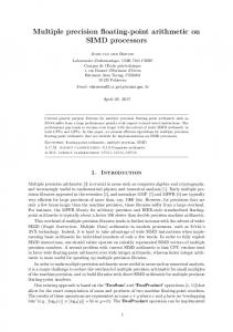
Quadword Load data
P0
S0
FPR: Primary
FPR: Secondary
P31
S31
Secondary
Primary: Scalar Side
Quadword Store data
Figure 1. Architecture of the BlueGene/L FP2 Core.
register files and memory. Each FP2 core occupies approximately 4% of the chip area, and consumes about 2 watts in power. Thus, creating the SIMD-like extension for both processors of the compute node doubles the peak floating point capability, at a modest cost in chip area and power, while doubling both the number of FPU registers and the width of the datapath between the CPU and the cache.
2.2. ISA enhancements The newly defined instructions include the typical SIMD parallel operations as well as cross, asymmetric, and complex operations. Table 1 shows a few exemplars. The asymmetric instructions perform different but related operations in the two datapaths, while the complex operations include symmetric and asymmetric instructions specifically targeted to accelerate complexarithmetic calculations. We have termed these new type of asymmetric instructions SIMOMD, for Single Instruction Multiple Operation Multiple Data. The asymmetric and complex instructions enable the efficient calculation of complex numbers as well as enhancing the performance of FFT and FFT-like codes. The cross instructions (and their memory-related counterparts, cross-load and cross-store) help efficiently implement the transpose operation and have been highly useful in implementing some of our new algorithms
3
for BLAS codes that involve novel data structures and deal with potentially misaligned data. Finally, the parallel instructions with replicated operands allow important scientific codes that use matrix-multiplication to make more efficient use of (always limited) memory bandwidth. The FP2 core supports parallel load operations, which load two consecutive double words from memory into a register pair in the primary and the secondary unit. Similarly, it supports an instruction for parallel store operations. The processor local bus of PPC440 supports 128 bit transfers, and these parallel load/store operations represent the fastest way to transfer data between the processor and the memory subsystem. Furthermore, the FP2 core supports a parallel load and swap instruction, which loads the first double word into the secondary unit register and the second double word into the primary unit register (and its counterpart for store operation). These instructions help implement the kernel for matrix transpose operation more efficiently.
0x00
0x04
0x08
0x0c
0x10
0x14
0x18
0x1c
ok ok ok ok ok ok
(a) 0x00
0x04
0x08
0x0c
0x10
0x14
0x18
0x1c
ok ok
(b) Figure 2. Alignment restrictions within a cache line on the PowerPC 440 FP2 Core. (a) Doubleword access. (b) Quadword access.
A[p|s]*Cp->Tp; A[p|s]*Cs->Ts). The function of the other permutations could be achieved through careful coding, and could often be achieved without performance penalty. For example, the permutations on the C operand could be achieved by using the four defined opcodes and interchanging the roles of the A and C operands. The load and store datapath pipes allow single precision or double precision data to be transferred between memory and the primary or secondary FPR file. Fortunately, the PowerPC 440G5 core is able to support the loading or storing of quadword operands in a single cycle. This allowed us to define instructions to simultaneously transfer doubleword data to or from both the primary and secondary register files. For efficient transfer, data must be word-aligned and must completely fit within a quadword-aligned quadword, as shown in Figure 2. This restriction exists because the cache architecture is such that it can transfer data from either one half of the cache line or the other. Each half is a quadword. Misalignments require that a trap handler artificially align the data within a half-line and then perform the access again. Thus, the penalty for misaligned data accesses is in the order of thousands of processor cycles. Sections 3.1 and 4.2 discuss how we proactively avoid this situation in the compiler and at algorithm design time. One compromise in the PowerPC 440 FP2 Core design is the lack of “D-form” loads and stores. The D-form instructions generate an effective address by adding the contents of a general-purpose register (GPR)—or zero—to a 16-bit immediate value. Unfortunately, the only way to fit this immediate value in the opcode is to use the portion of the instruction normally used to hold the secondary opcode. While the 16-bit immediate values add a lot of flexibility, each
2.3. Implementation issues The dual-issue nature of the CPU allows the initiation in each cycle of a quadword (i.e., two doublewords) load in parallel with two FMAs, yielding a peak performance of four floating-point operations per cycle. Latency and throughput for the new instructions are the same as that for the similar PowerPC floating-point instructions in the PowerPC 440 FPU. Also, like the PowerPC 440 FPU, there is no hardware register renaming. In order to avoid excessively depleting the opcode space allocated for APUs, the unit performs only double-precision arithmetic operations. This does not affect performance because the latency of all of the instructions (except for divide) is precision-independent. Load and store operations convert single-precision operands to double-precision as they enter the unit. Thus, applications that can get by with the reduced precision of single-precision raw data can consume less of the system’s overall memory bandwidth. To further economize on opcodes, we chose to limit the permutations of operand swapping. For example, the computational crossbar allows 16 variations on the parallel-multiply instruction by permuting on the source of the A and C operands (i.e., A[p|s]*C[p|s]->Tp; A[p|s]*C[p|s]->Ts). However, analysis of our target algorithms revealed that they generally needed only the four basic variations of permuting on the source of the A operands (i.e.,
4
FMA instr. class
Example
Parallel
fpmadd
fT,fA,fC,fB
Cross
fxmadd
fT,fA,fC,fB
Replicated
fxcpmadd
fT,fA,fC,fB
Asymmetric
fxcpnpma
fT,fA,fC,fB
Complex
fxcxnpma
fT,fA,fC,fB
Operation PT = PA ∗ PC + PB ST = SA ∗ SC + SB PT = PA ∗ SC + PB ST = SA ∗ P C + SB PT = PA ∗ PC + PB ST = P A ∗ SC + SB PT = −PA ∗ PC + PB ST = P A ∗ SC + SB PT = −SA ∗ SC + PB ST = SA ∗ P C + SB
C99 builtins
T= fpmadd(B,C,A) T= fxmadd(B,C,A) T= fxcpmadd(B,C,ap ) T= fxcpnpma(B,C,ap ) T= fxcxnpma(B,C,as )
Table 1. SIMOMD FMA instructions. We show representative instructions for each of the four classes of operations, their semantics, and their bindings to C99 builtin functions.
D-form operation—by virtue of reserving all ten secondary opcode bits—consumes the space of 1024 opcodes. Since we wanted to leave opcodes for other APUs, we decided to forgo these instructions. Instead, we support indexed instructions wherein the effective memory address is determined by the sum of two GPRs, or the value in a single GPR. The compiler team felt that the lack of D-form load/stores would affect performance due to the need for extra integer registers to hold the displacements. This hypothesis was tested by forcing the compiler to generate X-form load/stores for all floating point load/stores for a SPEC2000 FP run at -O3 on a PowerPC Power4 machine. The results showed an average of 5.5% decrease in SPEC2000 FP performance. This result is worse than a PowerPC 440 FP2 Core would experience, since primary load/stores could still use D-form load/stores.
logic was largely copied from the PowerPC 440 FPU Core, nontrivial changes were needed to handle bypass cases between single pipe instructions and dual pipe instructions. Since we started with a fully-verified core, we were able to start simulations early and attack corner cases of the new design.
3. Compilation Code generation for the PowerPC 440 FP2 Core is done within the TOBEY backend [19] of the IBM XL family of compilers for Fortran, C, and C++. TOBEY has been enhanced to schedule instructions for the PowerPC 440 FPU Core, and to generate parallel operations for PowerPC 440 FP2 Core using extensions to Larsen and Amarasinghe’s Superword Level Parallelism (SLP) algorithm [15]. This required the use of non-trivial extensions to the SLP algorithm to generate Cross, Asymmetric, and Complex SIMD-like instructions, and to exploit the additional set of FPU registers under the constraints of the instruction set architecture. Generation of parallel code is done late in TOBEY, just before scheduling and register allocation. The SLP algorithm works within a basic block. Consecutive loads and stores are paired up by matching base registers and displacements, and use/def chains are used to find additional candidate instructions for pairing. Each candidate pair is evaluated to see if generating the paired instruction is more efficient than the sequential instructions. A paired instruction is considered more efficient if it requires no extra moves to put the operands into the correct registers. For each instruction, the estimated bene-
The implementation reused much of the logic and layout from the PowerPC 440 FPU Core design. The computational datapath from the PowerPC 440 FPU Core was copied to form primary and secondary versions in the PowerPC 440 FP2 Core. These datapath pipes make up approximately 70% of the PowerPC 440 FP2 Core logic (excluding the register files), and their layout was largely derived from the PowerPC 440 FPU Core. Not only did this drastically reduce development time and required resources, but it also helped simplify our verification effort. Verification did not have to focus on the correctness of the datapath pipes. Instead, the simulation effort targeted changes in the datapath controls. Although the operand hazard/dependency control
5
fit is incremented if the operand is known to be in the correct primary/secondary register (because previously generated instructions have placed them there) or if they are unknown (the register allocator will allocate them properly). Operands known to be in incorrect registers decrease the estimated benefit. Each instruction may only appear in one parallel instruction. Our implementation generates all viable instruction pairs, and then uses a Briggs coloring algorithm [3] to find the sets of paired instructions where no instruction is in more than one pair. The benefit for each set of pairs is then recalculated, and the set with the largest benefit is selected. This is repeated until no more paired instructions can be found in a block. The original SLP algorithm at this point combines paired instructions to form larger sets, but this step can be skipped for the PowerPC 440 FP2 Core because it has only two-way SIMD parallelism. Instructions are then scheduled to find a consistent ordering. The implementation of the SLP algorithm is somewhat complicated by the existence of asymmetrical instructions in the PowerPC 440 FP2 Core instruction set. These introduce more possible instruction pairs, complicating generation and estimation of the benefits of each instruction. An example of this is the fxcsmadd instruction. It can be replaced by a fxcxma instruction by swapping the C operands. The benefit of the instruction is calculated for both variants, and the better one is used. In addition, the C and Fortran front-ends have been enhanced with builtin functions for generating the PowerPC 440 FP2 Core parallel instructions, exploiting the complex*16 type in Fortran and double _Complex type in C99. The builtin functions are unavailable in C++, as that language does not support a builtin complex data type. Section 4 contains an example of the use of these facilities.
address expression is aligned at a specific location in the program via a builtin procedure: void alignx(int alignment, const void *ptr). The compiler trusts this assertion and does not generate code to check it at runtime. We have extended the runtime to provide a special malloc routine which returns a 16-byte aligned location from the heap. We are in the process of extending the Toronto Portable Optimizer (TPO) component (the middle tier, machine-independent optimizer, shared by the Fortran, C, and C++ compilers) to propagate alignment information about pointer targets interprocedurally, as an extension to the interprocedural pointer analysis framework in TPO. We are also in the process of integrating a recently developed framework for automatic program transformations, in case of potential misalignment of data, to enable generation of SIMD instructions, including parallel loads and stores [7].
3.2. Optimization of reductions The original SLP algorithm is unable to pair instructions that have a true dependence between them, such as an FMA chain for sum reduction. We can break the true dependencies between every set of two instructions if we add temporary registers, facilitating the SLP optimization to pair it up. When the SLP algorithm discovers a true dependence between two isomorphic instructions, TOBEY transforms them as described above if they are part of a reducible chain. This optimization is performed only if strictness is disabled for the procedure. TOBEY currently detects chains of FMA, FP negate multiply subtract (fnms), FP multiply subtract (fms), and FP negate multiply add (fnma), pairing them up using their parallel equivalents. fms and fnma chains require the data in the array to be aligned because they need a cross move between the primary and secondary registers, costing an extra operation. Parallel loads on the data are needed for the reduction to be beneficial.
3.1. Avoiding alignment traps Section 2.3 discusses the high penalty for alignment traps on this architecture. To minimize alignment traps, TOBEY aligns data of size 16 bytes or more on a 16byte boundary for stack locals and externally defined data. Generation of parallel load/store instructions is suppressed unless it can be determined by examination of the alignment information on memory references that the instruction will not trap. Alignment information is available for local variables and for external variables defined in the current compilation unit. In many cases, it is not possible for the compiler to tell if a pointer points to aligned data. In this case, a user can assert that a given
3.3. Register allocation The challenges in register allocation relate to register pairing in parallel instructions. TOBEY’s intermediate representation uses an infinite supply of symbolic registers which then are colored to use a finite set of real registers. The secondary FP registers are treated the same as the primary ones. The instruction descriptions enforce pairing of one primary with corresponding secondary operand. For example a parallel load LPFL fp500,fp501=Memory(....)
6
describes that the first two operands are paired. fp500 must be a primary register and fp501 must be secondary. Both symbolic registers are also recorded as an aligned pair. The register coloring mechanism, based on Briggs’ register coloring algorithm [3], is modified to allow coloring of register pairs. Additional nodes are added to the interference graph, one for each real hardware register. When building the interference graph, each symbolic register used where a primary (resp., secondary) register is required has an interference edge added to all real hardware registers that are not valid primary (resp., secondary) registers. These new interferences restrict the symbolic registers to their corresponding register subset. Following the construction of the interference graph, nodes (representing registers) are removed from the graph one by one starting with the lowest degree nodes. As long as there is a node with degree smaller than number of physical registers, it is guaranteed to color and can be reduced. If there is none, a heuristic is used to select a node to spill. The removed or spilled node is put on top of the reduction stack. To help in assigning colors for pairs, reduced registers that are paired are set aside until their partner register is reduced before they are put on the reduction stack. Once both members of the pair are reduced, the two registers are pushed onto the reduction stack together. When the interference graph is completely reduced, registers are popped off the reduction stack and assigned colors. In the modified algorithm, the hardware registers are assigned colors first in order. This assigns each color a primary/secondary attribute as well as matches each color with its aligned partner. As the symbolic registers are popped off the reduction stack they are assigned colors according to Briggs’ algorithm. A symbolic register that is a member of a pair is popped off the reduction stack with its partner. The two registers are then assigned colors together, thus ensuring a valid color pair. Another challenge is combining two spill loads/stores into a parallel load/store. Intermediate spill instructions with compatible paired registers are combined first, and only afterwards is space dedicated in the spill area. An execution count estimate is used to prioritize combining of these spill locations. The remaining challenge is to rematerialize parallel loads as individuals. Memory locations determined as constant are added to rematerialization table. A parallel load, such as in the previous example, will also generate two individual entries (fp500 and fp501) using scalar load instructions. With these additional entries,
these two registers can be rematerialized if needed individually.
3.4. Future work PowerPC 440 FP2 Core provides parallel load instructions that can load successive floating point values into the primary and secondary registers either as or pairs. This decision has to be made in the first phase of the SLP algorithm, and will change the estimated savings benefits for future pairs of instructions. It might turn out that this will prevent parallel code from being generated. An algorithm to estimate the potential benefits of each load before the load has to be chosen. The current SLP algorithm generates code for each basic block independently. The SLP algorithm must be enhanced to support extended basic blocks. This may allow more parallel instructions to be generated. When pointer alignment is unknown, the compiler could generate a test of the address, and peel off a loop iteration to go to a known alignment. After this stage, __alignx directives can be used to tell TOBEY that the alignment is now known. This will generate additional loop bodies, and should only be done at high optimization or when the loop is known to be a hot spot. Applying this to multiple pointers is likely to be impractical due to exponential code growth.
4. Algorithms This section discusses several important ideas in the design of high-performance basic linear algebra subroutines (BLAS) and elementary functions that exploit the unique characteristics of the PowerPC 440 FP2 Core while steering clear of potential pitfalls with large performance penalty. Space limitations force us to restrict our discussion to three examples: matrix multiplication, a key Level 3 BLAS [6] kernel whose data reuse allows near-peak floating-point performance to be reached (Section 4.1); daxpy, a representative Level 1 BLAS [16] kernel where performance is limited by the memory bandwidth and data alignment becomes important (Section 4.2); and a vectorized square root operation, which is representative of mathematical routines whose use of data-dependent conditionals make them difficult to vectorize (Section 4.3).
7
4.1. Matrix multiplication: C ← αC + βA · B
its 7 stream limit, we will prepare both the A and B matrices. The pattern of matrix multiplication requires that we access rows of A and columns of B. As maximizing the number of independent dot-products in the inner kernel dictates the use of an outer-product matrixmultiplication algorithm at the register level, the format of these two sub-matrices is prescribed. The PowerPC 440 unit has 32 floating point registers (FPRs) and it is capable of performing one load/one store and one FMA, in parallel, in one cycle for data residing in the L1 cache. In practice, loads, calculations, and stores are staggered (i.e. preloads are performed) in such a manner so as to allow the floating point pipeline to “flow” efficiently. Thus it follows that d0 = e0 = 4 is a good choice as this utilizes 24 FPRs. In practice, some registers are used for level 3 prefetching so that the initial loading of the submatrix operands will be overlapped with computation. Note that streaming, provided by the hardware, is a form of level3 prefetching. In order to minimize the impact of latency, consecutive d0 × e0 updates are interleaved and overlapped so that the time between the load and use of the registers hoding the A and B submatrices can be increased.
Traditionally, high-performance matrix multiplication algorithms have involved the use of a kernel routine that takes advantage of the low-latency and high-badwidth L1 cache. Several approaches to blocking for this routine at higher levels of memory have been published in the literature [9, 10, 20, 22]. For example, if the A matrix is of size M × K, the A, a blocking of this matrix yields sub-matrices (blocks) that are of size M B × KB. For the L1 level of memory, our model indicates that one should load most of the L1 cache with either the A or the B matrix operand. The other operands, C, and B or A, respectively, are streamed into and out of (through) the remainder of the L1 cache while the large A or B operand remains consistently cache-resident. By “streaming” we mean the data for C and B (C and A) enters the L1 cache in the best possible manner, i.e. stride-one. Our kernel places the B operand, of size KB × N B, into the L1 cache, filling most of the L1 cache. However, we can stream m1 = M/M B blocks of size M B × N B and M B × KB, of C and A, respectively, through the L1 cache. By selecting M B based on the register sizes, we can allow M to be, essentially, infinite. We observe two practical benefits from our form of kernel construction and usage: (1) A rectangular blocking where N B < KB leads to a higher FLOP rate, due to the inherent asymmetry that results from the fact that we have to load and store C. (2) The streaming feature allows a factor of M/M B fewer invocations of the kernel routine.
4.1.2. In Practice: The PowerPC 440 FP2 Core L1 kernel Given the nature of the architecture, we want to use to PowerPC 440 FP2 Core as a SIMD vector machine, of vector length two. Conceptually, this can be realized by performing 2 by 2 by 1 submatrix computations on 2 by 2 submatrices. Let us choose the A matrix to hold vectors of length 2. The B matrix will also hold vectors of length 2; however, the components of B will be used as scale factors. A simple example will clarify what we have in mind. We compute the first column ofµ C(i:i+1,j:j+1) ¶= a(i, l) ∗ A(i:i+1,l:l+1) * B(l:l+1, j:j+1) as a(i + 1, l) ¶ µ a(i, l + 1) ∗ b(l + 1, j) and calcub(l, j) + a(i + 1, l + 1) late the second column in a similar fashion, using the two scalars, b(l:l+1,j+1). In order to respect the cache line size, we have designed our inner kernel as two k-interleaved 4 × 2 × 8 (m0 × k0 × n0 ) matrix multiplications. Even though this architecture exhibits extremely good latency characteristics, we load the non-cache resident matrix, A in 4 × 4 “chunks.” This yields a latency tolerance greater than 44 cycles for elements of A and greater than 20 cycles for elements of B, the cache-resident matrix. As the cold
4.1.1. In Theory: The PowerPC 440 FPU Core L1 kernel We sketch how to optimally implement a matrix multiply kernel for C = C + A · B under the assumption that its matrix operands map well into the L1 cache. Only a register block, a panel, and a resident matrix will occupy the L1 cache during a given time interval. See [1, 10, 11] for further details. The amount of memory at the L0 level equals the number of registers. Let a d0 × e0 block should occupy “most” of the registers and be used to hold a d0 × e0 submatrix of C while the remainder of the registers are used to stream in row/column elements of A and B. This requires d0 ∗ e0 + d0 + e0 FPRs. Registers can be loaded more efficiently from contiguous memory. Traditionally this has meant “preparing A,” stored by column (the result is AT ), by storing it by row, and computing C = C + (AT )T · B. In order to take advantage of the L2 cache’s pre-fetching abilities and not exceed
8
2i
2i + 1
x
P
S
y
P
S
x
y
(a)
P
2i
2i + 1
S
P
S
P
case is illustrated in Figure 3(b). Assume, without loss of generality, that vector y is aligned and vector x is not. Then vector elements y2i and y2i+1 are computed as follows.
S
1. Assume that registers P0 and S0 contain x2i−1 and x2i .
(b)
2. Load y2i into register S1 and y2i+1 into register P1 using a cross load.
Figure 3. Alignment possibilities in daxpy. (a) Vectors x and y are both quadwordaligned. (b) Vectors x is misaligned, while y is quadword-aligned.
3. Perform an fxcpmadd operation: P3/S3 = α· P0/S0 + P1/S1. Register S3 contains αx2i + y2i , while register P3 contains junk. 4. Load x2i+1 and x2i+2 into registers P0 and S0 using a parallel load. (This operation also sets up the required precondition for i + 1.)
load time from the L2 cache to the registers is no more than 18 cycles, this should allow the inner loop of our algorithm to proceed at the peak rate of the machine. The extra latency tolerance is built into the algorithm, so as to cover most of L3 latency for the non-resident, A matrix. The 20 cycle latency coverage for the cache resident matrix is advisable because the L2 prefetch stream dictates that the first load of a column block of B will result in an L2 miss and we wish to tolerate that as well.
5. Perform a scalar FMA: P3 = α· P0 + P1. Register P3 now contains αx2i+1 + y2i+1 . 6. Store y2i and y2i+1 to memory from register pair P3/S3 using a cross store. Thus, we have exploited the inherent 3:1 imbalance in memory accesses to FMAs in this operation to perform redundant floating-point operations while operating at peak cache bandwidth. With four-way loop unrolling and software pipelining, these operations can be scheduled to initiate a quadword load or store at each cycle. Note the critical use of the cross-loads and crossstores on the y vector, and the use of redundant computation to compensate for the relative misalignment between x and y. More elaborate versions of this technique are used when computing the dot product of two vectors and when computing a matrix-vector product.
4.2. Daxpy: y ← αx + y The BLAS-1 routine daxpy adds to vector y a multiple of vector x. Unlike the matrix multiplication routine, there is no reuse of the vector arguments, and the computation of a single element of the result involves two loads, an FMA, and a store. Performance is therefore limited by the speed at which data can be transferred between the memory hierarchy and the register file, and it is therefore important to use quadword loads and stores. Given the substantial penalty for unaligned quadword accesses, the overriding issue in gaining efficiency for daxpy is that of being able to maintain quadword access to and from memory irrespective of the alignment of the x and y vectors (assuming that these are stored contiguously in memory). Depending on the alignments of vectors x and y, there are four possibilities. When both vectors are quadword-aligned, it is trivial to perform quadword loads / stores and SIMD FMAs. If both vectors are misaligned, the first element is “peeled”, thereby aligning the remaining subvectors. This situation is illustrated in Figure 3(a). The more interesting case arises when one vector is quadword-aligned while the other is not. This situation can arise, for instance, with successive rows of a C array with an odd number of columns, or successive columns of a Fortran array with an odd-sized leading dimension. This
4.3. Square root: branchless programming The two-way SIMD nature of the PowerPC 440 FP2 Core and the pipeline depth of five cycles means that code with ten-way independence can in principle keep the floating-point processor busy at peak performance. Consider scheduling a collection of ten independent square root (sqrt) operations on this unit. The implementation of the intrinsic function sqrt generally looks something like this.
double sqrt(double x) { if (x != 0.0) r = x * rsqrt(x); else r = 0.0; return r; } The conditional branch in the code breaks up the ten instances of this operation into about 20 basic blocks
9
which the compiler is unable to schedule (recall that the SLP algorithm works only on basic blocks). The hardware supports a “parallel select” instruction, which implements a two-way parallel version of C’s ternary operation x?y:z in a pipelined manner. The sqrt intrinsic, when expressed using this method to handle its special cases, results in 100% utilization on the ten-way independent collection, compared to roughly 10% utilization for similar code using compare and branch. The compiler schedules instructions the same way for a user-written function declared inline as it does for the intrinsic function. It can therefore be worth expressing code which computes several candidate results and then selects amongst them, rather than choosing ahead of time which to evaluate. We have built a small library of Math intrinsic routines, including reciprocal, square-root, and reciprocal square-root operations.
FP2 Core instructions, making the compiler responsible for instruction scheduling and register allocation. 2 This version, in addition to containing the information present in version 1, incorporates loop unrolling and software pipelining to help the compiler identify PowerPC 440 FP2 Core operations and to reduce pipeline stalls. We present performance results for DAXPY, DGEMV, matrix-matrix product, and vectorized square root in Figure 4. The data reveals several trends. 1. Figure 4(a) demonstrates that the relative performance of small daxpy routines can be virtually insensitive to data alignment. In one case, the vectors are both misaligned and in the other they are both aligned. Figure 4(b) shows that this trend continues when the vector sizes become large. 2. The compiler gives relatively good performance when given data alignment and pointer alias information in many situations, but when instruction scheduling and cache hierarchy blocking are extremely important, it does not match hand-tuned code.
5. Experimental Results We now describe the performance of various computational kernels on the first BlueGene/L hardware prototype. This prototype runs at 500 MHz, and consists of 512 compute nodes, each with 256 MB memory. We limit ourselves to describing the results obtained on a single node of the BlueGene/L system, since our focus in this work has been on exploiting the dual-issue floating point unit. Clearly, the performance results we have obtained on these computational kernels have been important for achieving high performance on parallel applications that use these kernels. To “measure” the programming effort involved, we coded multiple versions of the test codes, as appropriate. Their nomenclature and descriptions are as follows. Unless otherwise stated, all codes are in C, and are compiled using the modified XL C compiler described in Section 3, with optimization level -O3.
3. Fixed overheads dominate the small problem-size running times of the advanced versions of the codes. 4. Figure 4(d) indicates that the architecture is capable of sustaining very close to peak performance when utilizing suitably blocked BLAS-3-like algorithms and the sensitivity of such algorithms to proper blocking. Note that these results reflect kernel speeds and do not take into account the overhead of data transformations.
6. Conclusions and Future Work At a very high level, high-performance engineering and scientific software can be viewed as an interaction among algorithms, compilers, and hardware. This paper is an illustration that such an interaction can produce a FPU and toolchain for engineering and scientific computations that can deliver a substantial fraction of its advertised peak performance. The PowerPC 440 FP2 Core hardware extends the PowerPC ISA in novel ways to support fast floatingpoint kernels, while being able to reuse much of the logic and layout of the PowerPC 440 FPU. The new design can run PowerPC floating-point code as well as code employing our new instructions, and effectively
0 The source code of this version contains no architecture-specific optimizations. 1 This version augments version 0 with alignment information (__alignx(16,x)) and pragmas asserting the absence of pointer aliasing (#pragma disjoint(*x,*y)). These enable the compiler to generate more PowerPC 440 FP2 Core instructions, particularly more parallel loads and stores. Additionally, this version modifies version 1 by using the C99 builtin functions shown in Table 1 to select PowerPC 440
10
Cycles Required
Cycles Required 1600
6 ´ 106
1400 1200
4 ´ 106
1000
Aligned
Aligned
800
2 ´ 106
Unaligned
600
Unaligned
400 Vector Length 200
400
600
800
1000
200000
400000
(a)
600000
800000
1 ´ 106
Vector Length
(b) Percentage of Peak 100
Cycles Required
Blocked
8 ´ 108
95
6 ´ 108
90
4 ´ 10
8
2 ´ 10
8
dgemmv0
Unblocked
85
dgemmv2
80
1000
2000
3000
4000
Vector Length
Matrix Order 100
(c)
200
300
400
500
(d)
Cycles Required 300000 250000 200000 150000
sqrtv_0 sqrtv_1 sqrtv_2
100000 50000
Vector Length 1000
2000
3000
4000
5000
(e) Figure 4. Running times for various versions of test codes on the PowerPC 440 FP2 Core. doubles the peak arithmetic and memory access performance of the core. The compiler for the unit extends both the SLP algorithm for parallelism detection and the Briggs register allocator to handle register pairs. The design of high-performance algorithms for this unit involves innovative techniques to balance the memory bandwidth and floating-point requirements of the operations without unnecessarily constraining data alignment. Initial results show that we are able to sustain a large fraction of the peak performance for key floating-point routines.
There are several possible directions for future work. On the hardware front, while the paired approach worked very well, we could effectively double the performance again had we added a second pair, and a means to keep the data fed. On the compiler front, Section 3.4 discusses several capabilities not yet in the compiler whose inclusion would enhance its capabilities. On the algorithm design front, there are many more operations for which we plan to design efficient algorithms.
11
References
[13] IBM Corporation. Book E: Enhanced PowerPC Architecture, March 2000. http://www3.ibm.com/chips/techlib/techlib.nsf/productfamilies/PowerPC. [14] IBM Corporation. PowerPC 440 Embedded Processor Core Users Manual, sa14-2523-01 edition, June 2001. available through IBM branch offices. [15] S. Larsen and S. P. Amarasinghe. Exploiting superword level parallelism with multimedia instruction sets. In SIGPLAN Conference on Programming Language Design and Implementation, pages 145–156, 2000. [16] C. L. Lawson, R. J. Hanson, D. R. Kincaid, and F. T. Krogh. Basic linear algebra subprograms for Fortran usage. ACM Trans. Math. Softw., 5(3):308–323, Sept. 1979. [17] R. K. Montoye, , E. Hokenek, and S. L. Runyon. Design of the IBM RISC System/6000 floating-point execution unit. IBM Journal of Research and Development, 34(1):59–70, 1990. [18] R. K. Montoye. Private Communication, Sept. 2001. [19] K. O’Brien, B. Hay, J. Minish, H. Schaffer, B. Schloss, A. Shepherd, and M. Zaleski. Advanced compiler technology for the RISC System/6000 architecture. In IBM RISC System/6000 Technology, pages 154–161, 1990. IBM Corporation. [20] R. C. Whaley and J. J. Dongarra. Automatically tuned linear algebra software. In Proceedings of the Proceedings of the IEEE/ACM SC98 Conference, page 38. IEEE Computer Society, 1998. [21] C.-L. Yang, B. Sano, and A. R. Lebeck. Exploiting parallelism in geometry processing with general purpose processors and floating-point SIMD instructions. IEEE Trans. Comput., 49(9), 2000. [22] K. Yotov, X. Li, G. Ren, M. Cibulskis, G. DeJong, M. Garzaran, D. Padua, K. Pingali, P. Stodghill, and P. Wu. A comparison of empirical and model-driven optimization. In Proceedings of the ACM SIGPLAN 2003 conference on Programming language design and implementation, pages 63–76. ACM Press, 2003.
[1] R. C. Agarwal, F. Gustavson, and M. Zubair. Exploiting functional parallelism on Power2 to design highperformance numerical algorithms. IBM Journal of Research and Development, 38(5):563–576, 1994. [2] G. Almasi, G. S. Almasi, D. Beece, R. Bellofatto, G. Bhanot, R. Bickford, M. Blumrich, A. A. Bright, J. Brunheroto, C. Cascaval, J. Casta˜nos, L. Ceze, P. Coteus, S. Chatterjee, D. Chen, G. Chiu, T. M. Cipolla, P. Crumley, A. Deutsch, M. B. Dombrowa, W. Donath, M. Eleftheriou, B. Fitch, J. Gagliano, A. Gara, R. Germain, M. E. Giampapa, M. Gupta, F. Gustavson, S. Hall, R. A. Haring, D. Heidel, P. Heidelberger, L. M. Herger, D. Hoenicke, R. D. Jackson, T. Jamal-Eddine, G. V. Kopcsay, A. P. Lanzetta, D. Lieber, M. Lu, M. Mendell, L. Mok, J. Moreira, B. J. Nathanson, M. Newton, M. Ohmacht, R. Rand, R. Regan, R. Sahoo, A. Sanomiya, E. Schenfeld, S. Singh, P. Song, B. D. Steinmacher-Burow, K. Strauss, R. Swetz, T. Takken, P. Vranas, and T. J. C. Ward. Cellular supercomputing with system-on-a-chip. In Proceedings of ISSCC’02, 2002. [3] P. Briggs. Register allocation via graph coloring. PhD thesis, Rice University, 1992. [4] K. Diefendorff et al. Altivec extension to PowerPC accelerates media processing. IEEE Micro, 20(2):85–89, 2000. Cahners Microdesign Resorces, 298 South Sunnyvale Avenue, Sunnyvale, CA 94086. [5] K. Dockser. “Honey, I Shrunk the Supercomputer” - The PowerPCTM 440 FPU brings supercomputing to IBM’s Blue LogicTM library. MicroNews, 7(4):29–31, November 2001. IBM Microelectronics. [6] J. J. Dongarra, J. Du Croz, S. Hammarling, and I. Duff. A set of level 3 basic linear algebra subprograms. ACM Trans. Math. Softw., 16(1):1–17, Mar. 1990. [7] A. Eichenberger, P. Wu, and K. O’Brien. Vectorization for short simd architectures with alignment constraints. In In Proc. SIGPLAN 2004 Conference on programming Language Design and Implementation, June 2004. [8] B. M. Fleisher. Private Communication, Sept. 2001. [9] K. Goto and R. A. van de Geijn. On reducing TLB misses in matrix multiplication. Technical Report CS-TR-0255, Department of Computer Sciences, The University of Texas at Austin, November 2002. [10] J. A. Gunnels, F. G. Gustavson, G. M. Henry, and R. A. van de Geijn. Flame: Formal linear algebra methods environment. ACM Transactions on Mathematical Software, 27(4):422–455, Dec. 2001. [11] F. G. Gustavson. New generalized matrix data structures lead to a variety of high-performance algorithms. In R. F. Boisvert and P. T. P. Tang, editors, The Architecture of Scientific Software. Kluwer Academic Press, 2001. [12] T. R. Halfhill. IBM PowerPC hits 1,000 MIPS. Microprocessor Report, 13(14), 1999.
12