oscillator is used as the clock for the PWM logic. An. Analog Devices AD9501 [3] digitally programmable delay generator is used as the interpolator. It provides a.
International International Conference Conference on Accelerator on Accelerator and Largeand Experimental Large Experimental Physics Control PhysicsSystems, Control1999, Systems Trieste, Italy
A HIGH-PRECISION PULSE-WIDTH MODULATOR SOURCE* F. Lenkszus, R. Laird, Advanced Photon Source, Argonne National Laboratory, Argonne, IL USA
Abstract A novel high-resolution pulse-width modulator (PWM) is being developed for a new digital regulator for the Advanced Photon Source power converters. The circuit features 82-ps setability over an 80-µs range. Our application requires a 50-µs full-scale range; therefore the 82-ps setability is equivalent to better than 19 bits. The circuit is presently implemented as a VME module and is an integral part of the digital regulator prototype. The design concept and performance results will be presented.
1 INTRODUCTION The Advanced Photon Source (APS) has initiated the development of a new power supply controller for the storage ring power supplies [1]. The storage ring uses 1500 power converters, one for each magnet (other than the main dipole bus). The present system uses an analog regulator with an analog PWM driving the power circuit insulated gate bipolar transistors (IGBTs). The new design will be a digital signal processor (DSP) based replacement for the existing regulator and controller. A key element of the new design is the PWM. This PWM is based on a digital counter with an interpolator. This offers the advantages of higher resolution, increased stability and less susceptibility to noise. In addition, an expensive high-resolution DAC used in the present design is eliminated. While the final digital regulator design will be a single board with an embedded processor, the first prototype is implemented in VME. The modularity offered by VME allows replacement of a function without replicating the entire circuit.
the PWM, since it must transition through “0” with minimum perturbation of the power supply output. The regulator stability is specified as residual rms current error to be –96 dB relative to maximum DC output in a 1-mHz to 2-kHz band.
3 CIRCUIT A block diagram illustrating the PWM concept is shown in Fig. 1. The PWM output is initiated by a start command that sets a flip-flop. The cascade of two timing circuits determines the width of the PWM output, a presettable digital counter followed by a digitally controlled interpolator. The counter and interpolator act as coarse and fine controls on the PWM output pulse width. The interpolator does just as its name implies; it interpolates between counter values to provide a finer step size than that yielded by the counter alone. One might ask, “Why not just use the counter alone?” The practical reality is that to achieve the same resolution as that of the circuit described would require a counter to operate at about 12 GHz. The stability of the PWM output width is largely determined by the stability of the oscillator used as the counter clock and the stability of the interpolator with time and temperature. Start
Synchronizer FF
Clock
Counter
PWM Out
Interpolator
Figure 1: PWM Block Diagram
2 SPECIFICATION The specification [2] calls for a “high precision digital PWM.” The PWM is to repeat its output at a 20-kHz rate with a usable resolution of 18 bits, guaranteed monotonic. The output is to be nominally adjustable from 0% to 100% duty cycle with allowance for minimum endstops. The new digital regulator will be used for quadrupoles, sextupoles and corrector magnet power supplies. Therefore, it must operate both in unipolar and bipolar modes. Bipolar operation places an additional demand on *Work supported by the U.S. Department of Energy, Office of Basic Energy Sciences, under contract No. W-31-109-ENG-38.
185
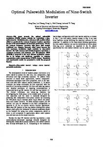
4 IMPLEMENTATION This prototype is implemented on a VME card. Figure 2 shows more detail on the actual implementation. Nearly all the digital logic is contained within programmable logic devices (PLDs). A 100-MHz oscillator is used as the clock for the PWM logic. An Analog Devices AD9501 [3] digitally programmable delay generator is used as the interpolator. It provides a digitally programmable delay that is used to interpolate between 100-MHz clock ticks. An external resistor and capacitor set the AD9501’s full-scale delay. In this case, since the total delay required from the AD9501 is small,
In Clk
Clk
PWM Out
8-Bit Shift Register 4
20kHz Start
D Clk
Q
Clk Clk
PWM FF
4-Input Mux
J Clk
Start Presettable Counter 13-bit Clk
Q
Clk K R
Sel TC
2-Bit Reg.
Synchronizer 13-Bit Register
Q
Offset Select
Coarse Width
Output Logic
Fine Width
Trig
Delay Out
AD9501 Interpolator
Reset
Mode
Polarity
Clk
100 MHz Osc.
Clk
Polarity
8-Bit Register
PLD
Mode
D Clk
A B C D
RExt
CExt RI
Figure 2. PWM Circuit Diagram
no external capacitor is required. The resistor is chosen to provide a total delay slightly greater than 20 ns. The reason for this will be explained later. A PWM cycle is initiated by the 20-kHz clock. This clock is synchronized with the 100-MHz clock via synchronizer flip-flops. The synchronized pulse starts the presettable counter. The value loaded in to this counter determines the “coarse” width. The start pulse is delayed via a shift register and multiplexer and sets the PWM flipflop that drives the PWM outputs. The terminal count output of the presettable counter triggers the AD9501, which provides the fine width control. Finally, the output of the AD9501 resets the PWM flip-flop, thus ending the PWM output pulse. The shift register/multiplexer combination is used to delay the setting of the PWM flip-flop relative to the counter start. This is to compensate to within one 100MHz clock tick for the minimum delay of the AD9501 and the propagation delays associated with getting the AD9501 output and trigger into and out of the PLD. This is necessary to achieve PWM output widths near zero with the coarse register preset to zero. Because of AD9501 part-to-part variations in minimum propagation delay, it is necessary to set the AD9501 fullscale delay to greater than 20 ns to ensure that the interpolation will cover an entire 100-MHz clock period. The PWM signal is combined with mode and polarity bits to generate four IGBT drive signals. Only the “A” output will be used for unipolar operation. All four outputs are used for bipolar operation to drive IGBTs in an “H” configuration.
186
5 CALIBRATION It is necessary to calibrate the fine width control so that it may be meshed monotonically with the coarse width set by the counter. The minimum and maximum fine width values needed to achieve monotonicity have been determined manually by observing the PWM output on a fast oscilloscope while DSP code toggles the PWM width between adjacent fine width steps. Since we will potentially be installing close to 1500 of these units, an automated procedure using the regulator DSP is highly desired. Once the entire regulator is installed in a power supply, it should be possible to automate PWM calibration using the power supply current readback as measured by regulator ADC. For bench testing, a simple calibration fixture consisting of an op-amp integrator with a gain of 200 has been used. This fixture integrates the PWM output pulse. The output of the integrator is fed into one of the 16-bit regulator ADCs. DSP code toggles the PWM output width between two values and reads in the digitized integrator output after a suitable settling time. It easily shown that, for a PWM repeat period much smaller that the integrator RC time constant, the change in integrator output voltage is given by:
∆V = −
R ∆t Vin , Rin T
where ∆t is the difference in PWM output pulse widths, T is the PWM repeat period, R/Rin is the integrator DC gain and ∆V is the resulting change in integrator output voltage. In our case for a gain of 200, PWM period of 50
µs, Vin of 5 volts, and minimum step size of 82 ps, the change in integrator output voltage is approximately 1.6 millivolts. This is easily detected via the 16-bit ADC and is potentially useful as part of a non-in situ automated calibration procedure.
6 PERFORMANCE The performance of the PWM circuit is largely determined by the two timing elements, the 100-MHz oscillator and the AD9501. In absolute terms, the oscillator stability would have to be better than 1.6 ppm to stay within the minimum step size of 82 ps at 50 µs fullscale. However, for the power supply regulator application, short-term relative stability is more important, and the oscillator stability requirements can be relaxed. Also, since the AD9501 is triggered by the counter terminal count, the AD9501 trigger input tracks drifts in the oscillator. Therefore, oscillator drifts will not cause monotonicity problems. The stability of the AD9501, on the other hand, is of more interest since drifts in its output could affect monotonicity. The data sheet specifies a typical temperature coefficient of 36 ps/°C for an AD9501 programmed to give 100 ns full scale. An application note [4] states a peak-to-peak jitter of 400 ps for a full-scale range of 100 ns. The PWM circuit uses a 100-ppm resistor to set the AD9501’s full-scale range. At a 21-ns full scale, a 100ppm resistor contributes about 2 ps/°C to temperature drift and therefore is not of concern. We used an environmental chamber to measure the drift characteristics of the VME PWM prototype and an AD9501in a simple circuit. The first measurement was done on an AD9501 that is part of a simple timing circuit not related to the PWM. Sampling oscilloscope probes were attached directly to the input and output pins of an AD9501. The temperature was changed plus and minus 10°C about 24°C. Measurements were made both at maximum delay (22 ns) and at about 30% of maximum. The temperature coefficient between input and output (delay through the AD9501) was measured to be approximately 30 ps/°C at maximum delay and about 20 ps/°C at the 30% delay. We also measured a jitter on the output of 158 ps peak-to-peak with a σ of 20 ps at maximum programmed delay. For the second measurement, we placed the entire VME crate containing the PWM unit and DSP processor in the environmental chamber and measured the stability of the PWM pulse width out the front panel of the VME card. The pulse width was set to approximately 478 ns. The AD9501 (fine width) was set to 50% of its full scale. A temperature coefficient of about 20 ps/°C for the pulse width was measured for a temperature change of 14 °C to 34 °C. The jitter in the pulse width was 158 ps peak-topeak with a σ of 24 ps.
187
For bipolar operation, the minimum achievable output pulse width is of interest. Measurements on the prototype yielded a minimum achievable stable output pulse width of approximately 4 ns. It appears that the fine width value to output pulse width becomes nonlinear below 6 to 8 ns. It is believed that this is due to the finite rise-time of the PLD PWM output interacting with the output driver.
7 CONCLUSION The PWM circuit presented offers better than 19 bits of effective resolution for a full scale output of 50 µs. Monotonicity in the output at 19-bit resolution will not be an issue as long as the ambient temperature does not change by more that 3 to 4 °C. The specified monotonicity requirement of 18 bits is met for our expected ambient temperature environment. The effect of long-term drifts in the interpolator on monotonicity is unknown at this time.
8 REFERENCES [1] F. Lenkszus, “State of the Art Developments in Accelerator Controls at the Advanced Photon Source,” PAC99, New York, NY, to be published. [2] J. Carwardine, private communication. [3] Analog Devices, Norwood, MA, 02062; http://www.analog.com [4] Application Note AN-260, Analog Devices, Norwood, MA, 02062; http://www.analog.com