non-cnherent architecture which enables the receiver to be extremely simple ..... Wireless Commu,iicorions Workrhop (FWCiV2003), Oulu, Finland, pp.121 - 124.
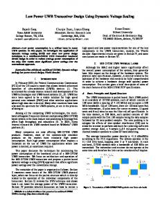
A LOW COMPLEXITY UWB CIRCUIT TRANSCEIVER ARCHITECTURE FOR LOW COST SENSOR TAG SYSTEMS Lucian Stoical, Sakari Tinraniemi, Heikki Repo', Alberto Rabbachin, Ian Oppermann
' Centre for Wireless Communications, University of Oulu, Tutkijantie 2 E, 90100, Oulu, Finland, Istoica63ee.oulu.fi
'Department of Electrical and Information Engineering, University of Oulu, Linnanmaa, BOX 4500, 90014, Oulu, Finland Abstract - This paper presents the architecture of a low power, low complexity Ultra Wideband (UWB) transceiver circuit. The circuit is designed for low data rate, low cost applications with built in location and tracking capabilities. The system is based on a non-cnherent architecture which enables the receiver to be extremely simple and largely insensitive to the transmitted pulse shape. The circuit presented contains the oscillator, the transmitter, the receiver and baseband digital signal processing (DSP) block. The oscillator contains the quartz oscillator, a delay locked-loop (DLL) and edge combiner for clock multiplication to generate a 528 MHz timing signal for pulse generation. The transmitter contains a second DLL to fix the delay of the UWB pulse, the UWB pulse generator and antenna. The transmined UWB pulse is presented. The receiver contains low noise amplifier, variable gain amplifier, squaring circuits, integrators for energy collection, 4 bit analogue-to-digital converters (ADC), digital control logic, integrator and gain selection logic block and detectionhit decision block. The circuits are designed in a 0.35 pm Si-Ge BiCMOS process from Austria Microsystems. Keywords - UWB transceiver, UWB pulse generator, DLL based clock synthesis.
I. INTRODUCTION Ultra wideband (UWB) is a very promising technology for future short-range indoor data communications applications [I]. The Federal Communications Commission (FCC) defines a radio system to be an UWB system ifthe fractional bandwidth Bf or the -10 dB bandwidth of the signal is greater than 20% or greater than 500 MHz, respectively [2]. The UWB concept can be based on time-hopping (TH), direct-sequence (DS) spread spectrum approaches, fast frequency sweeping, or multi-carrier techniques. The data modulation schemes most oflen used in UWB systems are pulse position modulation (PPM) and pulse amplitude modulation (PAM). The system concept is to have an indoor network with data rates of the order of 1 kbps - 100 kbps, an unlimited number of TAGS, a low power, low-cost, low-complexity UWB transceiver. The system concept utilize individual identification of each unit, 1 measurementisecond per unit, centralized control and positioning calculation in base stations, operation in unlicensed bands and two way data transfer sufficient to allow position information to be
0-7803-8523-3/04/%20.0002004 IEEE.
relayed. Also, device mobility is supposed to be slow (less than 40 kmm) and they have the possibility to joinileave the measurement area at arbitrary times. The stated intention is to he able to track devices in a specified measurement area for later processing or online monitoring purposes. The bandwidth of the UWB signal means that the number of the distinguished multipath components is very large [3]. This characteristic can give a gain both in terms of diversity and accuracy. In order to be able to exploit both advantages a higher implementation complexity is needed. In order to gain diversity it means to implement a RAKE receiver with a larger number of fingers and to implement an algorithm to search the strongest path. On the other hand to exploit the accuracy a very high frequency clock able to sample inside a sub-nanosecond time window is needed. Using such a high frequency clock, on the order of gigahertz, is not appropriate for implementing a low-power UWB TAG transceiver. The low complexity, low cost and low power UWB transceiver design targets combined with channel characteristics gives the idea to simplify the transceiver as much as possible and let all the computation capability to the base station. To achieve a reasonable BER for reasonable SNR we must design a robust receiver inside UWB TAG. The simplest choice to be designed is the energy collection approach which is able to recover the energy coming from the rich multipath channel. This noncoherent approach avoids requiring the implementation of channel estimation with the drawback of noise and interference enhancement. Because the modulation has no correlation in the receiver it needs to be orthogonal in the time domain. The duty cycle ratio of UWB TAG is 1% because it is transmittingireceiving 5000 bits to/from UWB base station 1000 us every 1 second. The above characteristic combined with low frequency reference oscillator make the low power implementation of UWB TAG feasible. The low-complexity of UWB TAG is given by the fact that DLL frequency synthesis approach is used [4] and at the receiver an architecture based on simple power integration circuit is employed. An UWB transceiver prototype which makes use of an architecture based on samplehold and A D converters was presented in [5]. The analogue-to-digital
196
Authorized licensed use limited to: IEEE Xplore. Downloaded on March 25, 2009 at 14:24 from IEEE Xplore. Restrictions apply.
conversion resolution used is 1 bit. An "all-digital" UWB receiver is presented in [6] where it is shown that the sufficient ADC resolution needed for reliable detection of a UWB signal is 4 bits. A UWB transceiver architecture and its typical performance parameters which is not based on impulse radio but on multiple bands are presented in [7]. The ADC resolution used in [7] is 6 bits. An time-modulated UWB receiver block diagram is presented in [SI where the ASIC implementation requirements of an integrated circuit correlator are determined. A much more complex digital processor module implemented in field programmable gate array (FPGA) technology which is used in a UWB transceiver is presented in [9]. A fully digital UWB receiver architectwe based on TH-PPM approach is presented in [IO]. In literature clock multiplication based on analogue approach which makes use of an monolithic inductorcapacitor (LC) tank to enhance the load impedance at the resonant frequency was reported in [4]. The disadvantage of using an LC tank in clock multiplication is that the multiplication factor is fixed and the large chip area is needed for inductor. Once the multiplication factor is decided the values for LC are fixed and they can not be modified An edge combiner based on digital gates was presented in [4], [4]. Our approach uses of AND-OR gates without using the OR idout buffer as in [12]. The paper is organized as follows: in section I1 the clock synthesis together with transmitter and receiver architectures are described, then section III and IV give the simulation results and the conclusions, respectively. 11. TRANSCEIVER ARCHITECTURE The UWB transceiver architecture for the UWB TAGS is based on a non-coherent structure utilizing bit position modulation (BPM) [13], [14].
1I 1 x 1
Fig. 1. Circuit architecture of UWB TAG
While sacrificing some performance in term of spectral efficiency, it greatly simplifies the implementation and decrease the size and cost of the circuit. The architecture for the UWB TAG transceiver is presented in Fig. 1. The UWB signal used for this study is based on a train of short.pulses multiplied by a spreading sequence using the direct sequence (DS) approach. The bit interval is divided into 2 time slots (binary modulation). As the detection procedure is based on energy collection, the separation of different users can only be done in the time domain. The transmitted signal for single user is given by equation (1).
where w,,.(t)is the transmitted pulse with pulse width T,. Tb is the symbol interval, S=125 ns is the delay used to distinguish different symbols and dn E [0,1] is the transmitted symbol. T, = NT, with N integer is the chip interval, and (c,), is the j "' chip of the pseuderandom (PR) code. The pseudo random (PR) code is bipolar with values (-1,+1).DatarateRdisdefinedhyl/Tb=1/(2S).
A. TRANSMITTER ARCHITECTURE The UWB transceiver clock generation is based on a 33 MHz crystal reference clock with high Q and DLL based frequency synthesis. Low reference clock frequency is used mainly because of low-power consumption requirements. For UWB system, timing is very important. Sub nanosecond pulses need to be transmitted using an accurate reference clock. Also at receiver, an accurate sampling is needed. In this paper we utilize one DLL plus edge combiner in order to avoid classic frequency synthesis with PLL and N divider. The DLL-based clock multiplication approach presented in Fig. 2 takes advantages of the inherently low jitter of a lowfrequency crystal oscillator reference to produce a lowphase-noise RF signal. This is accomplished by taking each relatively jitter-fiee but infrequent edge of the crystal oscillator output and from that generating a burst of wellcontrolled evenly spaced edges that span one period of the crystal oscillator. These evenly-spaced edges are combined by the AND-OR edge combiner to form a higher-frequency clock signal. The phase detector generates UPiDOWN signals according with the phase difference between the reference signal and the voltage controlled delay line's (VCDL) final stage output. The phase detector architecture was presented in [15]. The DLL-CM is in locked condition, if the input and output of the voltage controlled delay line are in phase. One delay cell contains two cascading CMOS inverters. Delay is adjusted by the charge pump and loop filter through control voltage such that to minimize the phase error. A classification of charge pump architectures is given in [16]. Our charge pump architecture is based on a single ended architecture with output active amplifier [16].
197
Authorized licensed use limited to: IEEE Xplore. Downloaded on March 25, 2009 at 14:24 from IEEE Xplore. Restrictions apply.
which have a fixed delay between them. Here, the two trigger signals are provided by DLL-PG as presented in Fig. 1, The short pulses generated by NAND-gates are converted into a differential signals by a micro-mixer [IS]. Two of these differential pulses with a fixed time delay are subtracted from each other in an analogue linear subtraction circuit. The output is a differential monocycle pulse with a typical pulse width of 500 ps.
C. RECEIVER ARCHITECTURE
+ + Edge Combiner
RF signal
528 MHz
Fig. 2. Clock synthesis based on DLL and edge combiner. The charge pump produces the control voltage needed to fix the delay edges of VCDL within range of phase error tolerated bv edge combiner. The control voltage controls the reference clock and fmal stage output of VCDL is 55 ps for all CMOS and temperature comers.
The receiver is based on a simple power integration circuit. It contains low noise amplifier (LNA), variable gain amplifier (VGA), multiplication and integration circuits and 4-bit N D converters, the digital control logic (DCL) and detectionibit decision block. The incoming UWB signal is amplified by the LNA, squared in by a multiplier and then integrated. This technique has the disadvantage that, as well as signal, noise is amplified at the receiver. The used widehand LNA was presented in [19]. It consists of a single stage in commonemitter configuration and an emitter follower in the feedback path. Flat frequency response and matching to 50 R are achieved by emitter degeneration and shunt feedback including Q1, L1, R2 andR3.
E. UWB Pulse Generator
The VGA was presented in [I91 and is based on Gilbert cell [20]. The gain may be vaned with a control voltage connected to the bases of the upper transistors. The control voltage range is from 1.36 V to 1.6 V, and the corresponding gain range is 36 dB from -17 dB to 19 dB, respectively. Two additional amplifier stages of the receiver contribute a fixed 40 dB gain, which gives a gain range from 40 dB to 75 dB for the receiver chain. The automatic gain control is digital so that there are four different control voltages and hence four different gain levels available. One of these is selected through monitoring the outputs of the AID converters. If more than one of the outputs has the maximum value of '1 1l', the gain is decreased, until only one achieves that value. On the other hand, if all of the outputs are at the minimum level, the gain is increased. The gain selection is made by the gain selection block as shown in Fig. 1. Receiver architecture contains a hank of 8 integrators. The integrator is a two stage integrator, which consists of a high-frequency Gm-C integrator presented in [21] and a differential operational amplifier in an inverting integrator configuration. Each of the integrators starts to collect the energy inside of a quarter of a bit time which is 30 ns. In order to have an accurate t e m g (start and stop instants) of the integration operation we make use of a digital control logic (DCL) based on eight 4 bit counters: one counter for each integrator. The principle of operation and results of DCL were presented in [19].
The UWB pulse generator used in transmitter is presented in [16]. The sttucture and performance are more or less identical due to the use of the same IC process. The pulse generator creates two short pulses from two trigger signals
The automatic gain control (AGC) loop contains the integrator and gain selection logic (IGSL), squaring circuit, variable gain amplifier, a hank of eight integrators and eight 4 bit AID converters. We use four integrators for energy
The function of the edge combiner is to take the outputs of the DLL and generate a 528 MHZ signal. For a clock multiplication of 16 we make use of 32 delay elements. Each delayed version DELAYi, i=1,..,32, of the reference clock is fed to the AND gate. Then each output of the AND gate, Ihj, j=l,..l6, is fed in the OR gate. The RF 528 MHz clock signal is produced at the output of the OR gate. In figure 3 the digital edge combiner based on AND-OR gates is presented.
DELAY i+
Fig. 3. Digital edge combiner element The second DLL (DLL-PG) is used to fix a delay of UWB pulse generator. The difference between DLL-CM and DLL-PG is that the voltage controlled delay line of DLL-PG generate 120 ps delayed edges compared with 2 ns delayed edges in DLL-CM.
198
Authorized licensed use limited to: IEEE Xplore. Downloaded on March 25, 2009 at 14:24 from IEEE Xplore. Restrictions apply.
collection together with four 4 bit AID converters for a bit time interval of 120 ns. The 4 bit AID converters make use of medium speed, medium accuracy successive approximation architecture (SAR) [ 2 2 ] .The bit time interval equal four times the clock reference period. The integrator and gain selection logic (IGSL) contains digital logic which implements the integrator selection based on the outputs given by 4 bit AID converters and gain selection on VGA. After the integrator selection is done by AGC, two energy collection values out of the integrators are fed into detectionibit decision logic block consisting of comparators. The detectionidecision block produces the resulting bit to be processed by the baseband DSP block. The base-band DSP logic contains digital logic which implements the MASTEWSLAVE functionality of UWB TAG. Also, the DSP logic controls the transmission of DLL-PG and LWEI pulse generator. In Fig. 4, the beacon detection block is presented. The signal coming kom integrators is converted to a digital value by the 4 bit AID converters. Based on these digital values the selection of the maximum value is done by the maxselection block. The maximum on position i, i=l,..8, trigger the numerator NUMI, i=1,..8. After 40 bits of preamble the maximum selection between the integrator outputs is done. If there are more than one winner the selection is made randomly based on modulo operation. If the value of numerators NUMi, i=l,..8, is bigger than a predefine threshold the preamble is considered to be detected. The synchronization is achieved if the beacon is detected twice.
Fig. 4. Beacon detection block 111. SIMULATION RESULTS
The transmitter architecture was tested independently with a 33 MHz clock input. The transmitted UWB pulse is presented in Fig. 7 . The typical pulse width is 500 ps. Digital selection of the detected winner integrator is presented in Fig. 5 . .itw*nw,
i
8
:
.
.. ..
.. ..
.
. i
, i
:
In Fig. 5 waveforms after the integrator winner detection are presented. Vector v contains a '1' in position i which means the winner is integrator number i, i=8,4 respectively. The basic state machine of the slave UWB TAG is presented in Fig. 6. Its functionality is described below. In DETECTION state, after PREAMBUI-SEARCH state, 63 bits are detected and then in BARKER-CORR state the barker correlation is executed in order to find the starting point of the information bits. Starting from this point the TAG counter counts 128 information bits and puts them in a receiving FIFO. In WAIT-FOR-SLOT-AFTERRX state first block of data is loaded from transmission FIFO in transmission register. The UWB TAG waits for the moment to transmit. It transmits slots of 128 bits when it receives the slot address from MAC layer. When transmission FIFO is empty the UWB TAG goes to WAIT-FOR-SLOT-AFTER-TX state. When the TAG is in WAIT-FOR-SLOT-AFTER_TX state and the guard period of 20 bits is empty the TAG goes to DETECTION state. In DETECTION state, after WAIT-FOR-SLOT-AFTER-TX state, the TAG detect 128 bits and puts them in receiving FIFO in LOAD-FIFO state.
_......, a n - s...., n, -.~
5%
Fig. 5 . Integrator winner detection RESEI
i Figure 6. Slave state machine for UWB TAG
199
Authorized licensed use limited to: IEEE Xplore. Downloaded on March 25, 2009 at 14:24 from IEEE Xplore. Restrictions apply.
.
. ..,.
,'. !
. ..
,
[XI
191
[IO]
,..
. [II ]
1121
Fig. 7. UWB Pulse out oftransmitter.
[I31
D. Dickran and P. Jett, "An application specific integrated circuit implementation of a multiple conelator for UWB radio applications", Proceedings qf Militaq Communications Co@rence. MILCOM IYVY. IEEE, vol. II,pp. 1207-10, October 1999. R. Fontana. A. Ameli and E. Richlry. L. Beard. D. Guy, "Recent Advances In Ultra Widehand Communications Systems". Proceedings qf IEEE Con/>rence on Ultra Widcbond Swrenis and Teechrdogiei, Baltimore. USA. May 2002. L. Stoica and I. Oppermann, "FPGA Implementation of a TimeHopping Pulse Position Modulation Design". Proceedirigs qf Fiinnirh Wireless Commu,iicorions Workrhop (FWCiV2003), Oulu, Finland, pp.121 - 124.October2003. C. Kim. I. Hwang, S. Kang, "A Low-Power Small-Area + 7 . 2 8 ~ ~ Jiner I-GHr DLL-Based Clock Generator", IEEE Joirmal qf Solid Store Circ~rits,vol. XXXVIl, no. I I , pp. 1414-1420. November2002. D. Foley. M. Flynn. "CMOS DLL-Based 2-V 3.2-pr Jitter I-GHz Clock Synthesizer and Temperature-Compensated Tunable Oscillator". IEEE JoirmalqfSolid-State Circuits, vol. XXXVI, no. 3, pp.417423, March2001 A. Rahhachin. R. Tesi and I. Oppermann. "Bit Error Rate Analysis for UWB Systems with a Law Complexity, Non-Coherent Energy Collection Receiver", accepted for publishing at IST, Lyon, France, 2004.
IV. CONCLUSIONS
In this paper a low complexity architecture of an UWB TAG circuit transceiver has been presented. Circuits are designed in 0.35 Si-Ge BiCMOS process technology. Simulation results show that frequency synthesis based on delay-locked loop and digital AND-OR edge combiner is feasible for generating timing for UWB pulse transmission with pulse width of 500 ps. The corresponding centre frequency of the pulse is 2 GHz and the bandwidth at -10dB is 4.03 GHz. Timing signals out of the integrator winner detection block were presented. Also, the UWB transmitted pulse is presented. The UWB beacon detection block and slave state machine for UWB TAG were also presented. REFERENCES M. Himillinen et. al. "On the UWB System Coexistence With GSMPOO, UMTSIWCDMA, and G P S , IEEE Josmol on Selected Aieos in Communicotions, vol. XX, no. 9, pp. 1712-1721, December 2002. FCC, First Report and Order, Apnl22.2002, FCC 02-48. J. Faerster and Q. Li, "UWB Channel Modelling Contnhution t o m Intel", IEEE P.802. IJ-02/279-SG3a. G. Chien and P.R. Gray, "A 900-MHz Local Oscillator Using a DLLBased Frequency Multiplier Technique for PCS Applications", IEEE Journol ofSolid -State Circuits, vol. XXXV, no. 12, pp. 1996-1999, December 2000. I. O'Donnell, M. Chen, S . Wan& and B. Brcdersen, "Ultra-Widehand Hardu,are Design". A n Ult?-o-Widebond Technology Workshop: From Research to Renliw. Los Angeles, USA, October 3-4'" 2002. P. P. Newaskar, R. Blazquez and A. P. Chandrakasan, "AID Precision Requirements For An Ultra-Widehand Radio Receiver", in Proceedings of IEEE Workshop on S i g d Processins Systems 2002 (SIPS '02). pp. 270-75. October 2002. G.R Aiello. "Challenges far ultra-wldehand (VWB) CMOS integration", Microwme Symposium Digest, 2UU3 IEEE MTTS Internotional, vol. I, pp. 8-13, June 2003.
1141 A. Rabhachin and I. Oppermann, "Synchronisation Analysis for U W B Systems with a Low-Complexity Energy Collection Receiver", accepted for publishing at 2004 brternotiorrol Workshop on Ultra Wideband System IWUBS 2004 (Joint UWBST&I WUWBS'2004). Kyoto, Japan, May 18-21,2004, [IS] B. Razavi, "Design of Analogue CMOS InteErated Circuits", McGraw-Hill Higher Education, Avenue of the Americas, New York, 2001 [I61 W. Rhee. "Design of High-Performance CMOS Charge Pumps in Phase-Locked Lwps", Proceedings qf the 1999 IEEE lnternationol Svniposiirni on Circuits and Swtemr ISCAS ,vol. 11, .~ a.e . 5 4 5 548,30 . . May-2 June 1999. I171. S. Tiuraniemi (20031 "CMOS Pulse Generator Design For TH-PPM . UWB System", Proceedings qf Finnish Wireless Communications Workshop (FWCW'OS), Oulu, Finland, pp.136 - 139, October 2003. [I81 B. Gilbert, "A Highly Linear Variant of The Gilbert Mixer Using a Bisymmetric Class-AB lnput Stage", IEEE Joirrnnl Of Solid Store Circuits. vol. XXXII, pp. 1412-1223, September 1997. 1191 L. Stoica. Sakari Tiuraniemi, Albert0 Rabhachin and I. Oppermann, "An Ultra Wideband TAG Circuit Transceiver Architecrure", accepted for publishing at 2004 International Workshop on Ultra Widebond Systems (Joint UWBST&IWUWES'2004). Kyoto, Japan, May 18-21,2004, 1201 B. Gilbert "A Precise Four Quadrant Multiplier With Sub Nanosecond Response", IEEE Journal Of Solid State Circuits. vol. 111, pp. 365373.1968. 1211 H. Khonamabadi, "High-Frequency CMOS Continuous-Time Filters", IEEE Joirrnol Of Solid Store Circsits, vol. XIX, pp.939-942. June 1984. 1221 D. Johns and K. Martin, "Anal~gueIntegrated Circuit Design", John Wile.v&Tonslnc, 1997. ~
200
Authorized licensed use limited to: IEEE Xplore. Downloaded on March 25, 2009 at 14:24 from IEEE Xplore. Restrictions apply.