Jun 28, 2009 - I. INTRODUCTION. Flash architecture based analog-to-digital converters ..... clock and data recovery circuit,â IEEE Symp. VLSI Circuits, pp.
A Multiplexer-Based Digital Passive Linear Counter (PLINCO) Skyler Weaver, Benjamin Hershberg, Pavan Kumar Hanumolu, and Un-Ku Moon School of EECS, Oregon State University, 1148 Kelley Engineering Center, Corvallis, OR 97331. USA.
Abstract—A passive linear counter (PLIN CO) is presented. By cascading many passive transmission-gate multiplexers, a circuit is created that takes any scrambled digital input and sorts it into a thermometer coded output. Another variation produces a “one-hot” coded output. The number of muxes, n, required for these circuits increases with O{n2 }, so a folding technique is presented that reduces the order to O{n log(n)}.
Vin
Vref
0 0 1 1 1 1 1
I. I NTRODUCTION Flash architecture based analog-to-digital converters (ADCs) are the perferred ADC architecture for high-speed applications [1][2]. Flash-based ADCs consist of an input that is connected to a set of comparators that are all given different references, which are equally spaced by a least-significant-bit (LSB) voltage. This can be achieved by using an equal-valued resistor string as shown in Fig. 1. Each clock cycle, every comparator produces either a “high” or “low” result (i.e. 1 or 0) depending on whether the input is higher or lower than the reference given to that comparator. This implies that there are 2N − 1 (where N is the number of bits) comparator outputs; however, if there is negligible comparator offset and the references are monotonic, then there will be only one transition between 1 and 0 outputs (thermometer code). The 1-to-0 transition can be found by adding digital XOR gates with one input connected to a comparator output and the other input connected to the adjacent comparator output. All XOR outputs will be 0 except for the XOR gate with differing inputs. This resulting code of all 0s and a single 1 is called a “one-hot code,” since only one wire has a digital 1. A one-hot coded result is typically converted to binary using a lookup-table ROM or a wired-OR matrix [1]. If comparator offset is large enough to not be negligible (or the monotonicity of the references is not guaranteed), then there can be “bubble errors” in this transition (1). Firstorder bubble errors (those occurring adjacent to the 1-to0 transition) can be easily corrected for, but if higher-order bubble errors can occur, a ones adder is required to sum all of the 1 outputs [3]. Since there is a steady trend in integrated circuits to be scaled in their dimensions [4][5], we can expect scaled transistor variability to increase at each new technology node [6]. This device variation leads to large random offsets in comparators; so large that it has been proposed to use random comparator offsets as comparator references (instead of a resistor string) [7][8][9]. Since in these designs there is no thermometer coded output, conventional digital adder trees [1][10] must be used. The power and area required for the ones adder is significant and can exceed that of the all
Vref
Vin 0 0 1 0 1 1 1
Vref
Vin 0 0 1 1 0 1 1
Fig. 1. On the left, a standard 3-bit flash analog-to-digital converter; the output is guaranteed to be a monotonic thermometer code. In the center, a first order “bubble” error due to random offsets in the comparators. On the right, a second order “bubble” error due to even larger random offsets being present.
Vref
Vin 1 0 1 1 0 1 0 0
0
0
1
1
1
1
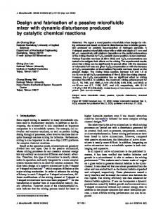
Fig. 2. A passive linear counter (PLINCO). The outputs of the comparators are the select lines for the muxes. If a select line is 0, the result is shifted to the right through that row of muxes. If the select line is 1, the result is shifted left. The thick lines represent digital 1s and the thin lines represent digital 0s. Note that the output of the PLINCO has the same number of 1s as the input (from the comparator outputs), but merely sorted into a thermometer code.
of the comparators. In this paper we present an alternative to a full-adder based ones adder by making a multiplexer-based structure that can perform the same function. II. T HERMOMETER CODE GENERATING PLINCO Combining multiplexers (muxes) as shown in Fig. 2 will create a circuit we are calling a passive linear counter (PLINCO), since the output is a count of the number 1s in the input,
A
B 1 1 1 0 1 1 1
S
S
S
0 0 0 1 0 0 0
(a)
Y Fig. 3. This is a passive transmission gate multiplexer. When the select line (S) is high (implying S is low), the input B is passed to the output Y . When S is low (S is high), then the input A is passed to Y .
Vref
1 1 1 0 1 1 1 0 0 0 1 0 0 0
Vin 1 0 1 1 0 1 0
(b)
1 1 1 0 1 1 1 0 0 0 1 0 0 0
(c)
7
6
5
4
3
2
1
0
Fig. 4. This is much like the thermometer code generating PLINCO, except it generates a one-hot coded output. The outputs of the comparators are again the select lines for the muxes; however, there is only a single digital 1 that is either shifted left or right through each row depending on whether the select line is 1 or 0, respectively. The thick lines represent the digital 1 and the thin lines represent digital 0s. Note that the output of the PLINCO is a single digital 1 where the position indicates the number of 1s that are in the input.
AB S
S
Fig. 6. a) The MSB of a one-hot-to-binary decoder for the PLINCO in Fig. 4, the outputs of the PLINCO are buffered with digital inverters which are used in the decoder. b) The 2nd MSB for the same one-hot-to-binary decoder. c) The LSB of the one-hot-to-binary decoder.
whether the select line is 0 or 1, respectively. If shifted left, a digital 1 is shifted in from the right; if shifted right, a digital 0 is shifted from the left. In this manner, after each row of muxes the digital word grows by one bit until the final output is the same length as the original PLINCO input; however, the output is now sorted into a perfect thermometer code. III. “O NE - HOT ” CODE GENERATING PLINCO
Y Fig. 5. This is a passive transmission gate mux with only PMOS transistors. This mux will quickly pass a digital 1, but will have difficult passing a digital 0. This simple mux can be used in the one-hot code generating PLINCO since the muxes either pass a digital 1 or pass nothing.
but the output is not inherently binary. In order to make this circuit passive (and more efficient), each digital mux is implemented as a passive transmission gate (Fig. 3). The input to the PLINCO here is the output of a 3-bit flash ADC with a nonmonotonic output (here the flash output is completely scrambled). Each comparator output is the select line for a row of muxes. The digital word that appears above a row of muxes is then shifted right or shifted left depending on
As indicated in the introduction, sometimes a thermometer code is less desireable than a one-hot code since the latter can feed directly into a lookup-table or wired-OR matrix. By merely flipping each mux upside-down, the result is a PLINCO that gives a one-hot coded output (Fig. 4). In this variation, the digital word in merely a single digital 1 and is shifted left or right depending on the next row’s select line. The final location of the single 1 in the digital output indicates its value. One advantage of the one-hot code generating PLINCO over the thermometer code generating PLINCO is that since each mux either propagates the single 1 or propagates nothing, the muxes do not need both NMOS and PMOS transmission paths. In fact, all of the muxes can be replaced with the simpler version shown in Fig. 5 (assuming that the outputs are reset to 0). Fig. 6 is an example one-hot-to-binary decoder for Fig. 4.
tra
tra
ex
ex (a)
possible outputs Fig. 7. After the single digital 1 of a one-hot PLINCO has rippled through eight rows of muxes, if the 1 location is known, then the muxes marked “extra” are gauranteed to not to recieve the digital 1.
IV. F OLDED PLINCO The two previous PLINCO architectures are very efficient for a small number of inputs, yet if the number of inputs (n) is very large, the number of muxes required increases with O{n2 }. This implies that area and power will be the same order. Also, since PLINCO is defined as being passive, each row of muxes increases the time-constant such that buffers should be placed every certain number (e.g. 8) of mux rows. To combat both the quadratic increase in area and the need for buffers, a PLINCO can be folded into cells of many smaller PLINCOs. Fig. 7 visualizes this motivation and the wasted area for a large number of inputs (imagine n = 1024). Adding some simple logic at the output of a PLINCO it is possible to both generate carry information to be processed elsewhere and the output of the logic will act as a buffer to the next stage. Fig. 8 is a folded PLINCO cell that has 8 outputs that is then folded by a factor of 2; the carry information is a single bit with weight of 4. Although we are using a cell with an 8output PLINCO with a folding factor of 2 in our example, other numbers of outputs and folding factors can be used. The carry information is then processed by another folded PLINCO (Fig. 9). This allows a folded PLINCO to have a regular cellbased structure to aid in layout. Area and power for a folded PLINCO will then follow O{n log(n)} dependence on the number of inputs, making it more viable when the number of inputs is very large. V. M AJORITY- VOTE PLINCO In some instances it is only important to know whether there are more 1s or more 0s, rather than the total number of 1s; we call this a majority-vote [11]. A majority-vote circuit can
(b)
Fig. 8. a) A folded PLINCO cell. The digital 1 enters at the top of the cell on one of the 4 wires. It ripples through 4 rows of muxes such that the digital 1 can be at any of the 8 outputs. Digital gates are used to fold the output by a factor of 2, either the 4 rightmost outputs are passed on to the next cell or the 4 leftmost outputs are passed on. A carry bit is generated that is either worth 0 or 4 and becomes the input of another folded PLINCO. b) This is a transistor level schematic of the same folded PLINCO cell. Note that the muxes are actually NMOS devices which are only able to pass digital 0s. In this case, a single 0 will ripple though the PLINCO, but the operation is the same. The blue lines indicate one possible path for the digital 0 to propagate through the cell. The grey transistors are merely there to reset the cell since the NMOS muxes can not pass a digital 1 easily.
be easily implemented as a PLINCO where only the middle of the thermometer code output is important, therefore the superfluous muxes can be removed. An example of a 7-input majority-vote PLINCO is shown in Fig. 10.
1 1 1 0
VI. C ONCLUSION
2 2 2
The passive linear counter was presented. If a flash ADC is designed and there is the possibility of high-order bubble errors, the designer must use a ones adder to decode the output. Typically a ones adder is a Wallace tree structure with ripple-carry adders and introduces significant delay, area, and power consumption. By introducing the PLINCO, a designer has another option to try an find an optimum design. In this paper we have proposed four variations of PLINCOs each with differing benefits. An exciting aspect of the PLINCO is the high design flexibility and the fact that it can be easily modified to be used in many applications.
PLINCO
2 8
Folding logic
2
2 2 2
PLINCO
2 8
inputs
Folding logic
2
Folded PLINCO cell
2 2 2
PLINCO
2 8
Folding logic
2
ACKNOWLEDGMENT
2 2 2
PLINCO
This work was supported by the Air Force Research Labs (AFRL), and Tektronix, Inc.
2 8
Folding logic
2
2
2
2
2
2
PLINCO
2
2
1 1 1 0
R EFERENCES
PLINCO
[1] F. Kaess et al., “New Encoding Scheme For High-Speed Flash ADC’s,” Circuits and Systems, IEEE International Symposium on, pp. 5-8, June 1997 [2] R. J. Van de Plassche, Integrated analog-to-digital and digital-to-analog converters, Kluwer Academics Publishers, ch. 3, 1994. [3] E. S¨ all, M. Vesterbacka, and K. O. Andersson, “A Study of Digital Decoders in Flash Analog-to-Digital Converters,” Circuits and Systems, IEEE International Symposium on, pp. 129-132, May 2004. [4] G. Moore, “Cramming More Components onto Integrated Circuits,” Electronics, vol. 38, no. 8, 1965, pp. 114-117. [5] B. Spencer, L. Wilson, and R. Doering, “The Semiconductor Technology Roadmap,” Future Fab Int’l, vol. 18, Jan. 12, 2005. [6] T.-C. Chen, “Overcoming Research Challenges for CMOS Scaling: Industry Directions,” Solid-State and Integrated Circuit Tech., Inter. Conf. on, pp. 4-7, October 2006. [7] C. Donovan and M. P. Flynn, “A ‘digital’ 6-bit ADC in 0.13 µm CMOS,” Solid-State Circuits, IEEE J. of, vol. 37, no. 3, pp. 432-437, Mar. 2002. [8] D. C. Daly and A. P. Chandrakasan, “A 6b 0.2-to-0.9V Highly Digital Flash ADC with Comparator Redundancy,” Solid-State Circuits Conf., IEEE Inter., pp. 554-555, 635, February 2008. [9] S. Weaver et al., “A 6b Stochastic Flash Analog-to-Digital Converter Without Calibration or Reference Ladder,” Solid-State Circuits Conf., IEEE Asian, November 2008. [10] C. S. Wallace, “A suggestion for a fast multiplier,” IEEE Trans. on Electronics Computers, pp. 14-17, Feb. 1964. [11] P. Hanumolu, G. Wei, and U. Moon, “A wide tracking range 0.2-4Gbps clock and data recovery circuit,” IEEE Symp. VLSI Circuits, pp. 88-89, Jun. 2006.
2 8
Binary decoder
3-bit output 6/28/2009
8
Binary decoder
(3-bit output)×4 Skyler Wea
Fig. 9. An example of a 20-input folded PLINCO. The folded PLINCO cell designated by the dashed box is the same circuit as Fig. 8. The top of each folded PLINCO chain is seeded with “1 1 1 0” since this is equivalent to a value of zero. The binary decoder blocks would be the same as Fig. 6 with the digital inverters reversed.
Vref
Vin 1 0 1 1 0 1 0 1
Fig. 10. A majority-vote PLINCO takes a number of digital inputs and outputs a digital 1 if there are more 1s present and a digital 0 if there are more 0s. This circuit is identical to Fig. 2 except the unnecessary muxes have been removed.