A New Digital Background Correction Algorithm with Non-Precision Calibration Signals for Pipelined ADCs Behzad Zeinali and Mohammad Yavari Integrated Circuits Design Laboratory Department of Electrical Engineering, Amirkabir University of Technology Tehran, Iran E-mails:
[email protected],
[email protected] Abstract—A new digital background calibration algorithm for pipelined analog-to-digital converters is proposed in this paper. It is based on error estimation with non-precision calibration signals for foreground correction and a modified split structure for converting the foreground structure to the background one. This architecture allows improving the calibration signals accuracy contrarily to linear gain error coefficient, while the modified split structure does not need matching between the two channels. The presented algorithm is investigated in system level in MATLAB for a 12-bit pipelined ADC. It achieves an improvement equal to 36.5 dB and 44.5 dB for SNDR and SFDR, respectively where the input signal frequency is 39 MHz with a 100 MHz sampling frequency.
I.
INTRODUCTION
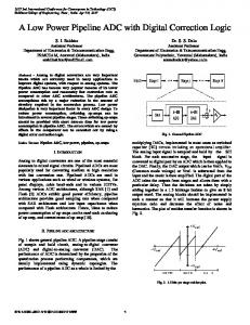
New generations of wireless communication systems highly demand for high-speed, high resolution, low-power and low-voltage analog-to-digital converters (ADCs). The Pipelined ADCs are the best candidate for resolutions between 10 to 16 bit and speeds between 15 MHz to 250 MHz [1]. Obviating these demands requires using deepsubmicron CMOS technologies, while those will involve us with the constraints that result in a limited resolution for ADCs. Such phenomena are mostly arisen by three different sources: capacitor mismatch, finite amplifier dc gain, and nonlinear behavior of the gain stage. These problems are aggravated by shrinking the technology size because in scaled-down CMOS, the transistor intrinsic gain (gmrds) and matching between the circuitry components decrease considerably. So, the digital calibration techniques have been presented for palliating the ADC constraints that can reduce the power consumption and relax the amplifier design process [1]–[7]. Also, the calibration process in digital domain is very interesting because digital circuits are fast and reliable in CMOS nano technologies. The digital calibration algorithms are majorly classified into two categories of foreground and background techniques. The foreground calibration interrupts the conversion of the input and enters the ADC into the calibration mode. On the other hand, the background calibration scheme doesn’t interrupt the conversion of the input signal; rather the calibration and digitization processes are done at the same time. A 12-bit pipelined ADC is shown in Fig. 1(a). It includes twelve 1.5-bit stages where its i-th stage is sketched in
978-1-4577-1846-5/11/$26.00 ©2011 IEEE
Figure 1. (a) 12-bit pipelined ADC architecture, (b) 1.5-bit gain stage.
Fig. 1(b) and also consists of a two-bit flash ADC, producing digital outputs as D1, D2, …, D14. Since the gain of each stage is not exactly equal to 2, a total of 13 stages are required to achieve 12-bit resolution. We do not have the front-end SHA circuit in this structure because of the additional noise and power consumption which it imposes to the circuit. Eliminating of SHA could be compensated by time matching technique between the MDAC and sub-ADC paths [2]. This paper presents a new digital background calibration algorithm for 1.5 bit per stages pipelined ADCs. It utilizes the LMS algorithm to estimate the error coefficients and improves the calibration signals accuracy contrarily to the gain error coefficient (α1). In addition, a modified split structure is proposed for changing the foreground algorithm to the background one. II.
CALIBRATION ALGORITHM IN FOREGROUND MODE
A. LMS-Based Algorithm Figure 2 shows the ADC structure in the calibration mode where the first stage non-idealities are modeled by a fifthorder polynomial, f5(.),and the other stages are assumed to be ideal. In this figure, Vr1 is the residue voltage of the first stage, Vd1 is its distorted value, Vout1 is the stage analog output and Dr1-desired, Dd1 and Dout1 are their digital values, respectively. The input of the first stage is connected to the ground and a two level dither signal, PN, is injected into the
418
Figure 2. Conventional foreground calibration mode of ADC.
input of sub-DAC. If f5(.) is a fifth-order polynomial, the first stage analog and digital outputs can be written as:
Vout 1 = 2[(1 − α 1 )Vr1 − α 3V r31 − α 5V r51 ]
Dd 1 = (1 − α1 ) Dr1−desired − α 3 D
3 r1− desired
− α5D
5 r1−desired
(1) (2)
Since we aim at estimating the first three odd error parameters (α1, α3 and α5), where these are noisy, using the mean squared error (MSE) criterion and least mean square (LMS) algorithm, four independent equations are required. So, the first stage 1.5-bit sub-DAC utilizes 8 different voltage levels (±V1, ±V2, ±V3 and ±V4=±VRef /2) in the calibration mode where they apply to DAC with control signals of ci, i={1,2,3,4}. The accuracy of estimation improves with increasing the number of voltages and their distances. We should note that the voltage levels (except VRef /2) in this sub-DAC must be implemented with the minimum backend accuracy and this is the most important drawback of the mentioned algorithm, e.g. the calibration of the first stage should be done when the voltage levels of sub-DAC have the minimum 13-bit accuracy. In conventional implementations, voltage levels with more than 10-bit accuracy cannot be easily generated, so, some methods should be used that eliminate more than 10-bit accuracy requirement in real implementations. B. Error estimation with non-precision calibration signals This method is inspired from the fact that the accuracy of ±VRef /2 is not important due to its usage in all sub-DACs in different stages. So, in calibration mode of each stage, if subDACs in next stages use the same voltage level, the effect of voltage offset or low frequency noise will no large seen. In Fig. 3, if the dither value is set to zero in the calibration mode, the output value of the first stage sub-DAC will be equal to -(Vi+εi) where i ={1,2,3,4} and Vi is the desired voltage level and εi is a random error produced by the fabrication process when Vi >> εi. Therefore, the output of the first gain stage feeding the second stage would be as:
Vout 1 ≈ 2[(1 − α 1 )(Vi + ε i ) − α 3Vi 3 − α 5Vi 5 ]
(3)
Figure 3. Proposed method for calibration of the first stage of ADC.
If Vi > VRef /8, then the second stage digital output will be equal to D2=10—it means the most significant bit (MSB) is 1 and least significant bit (LSB) is 0—and if the sub-DAC of the second stage utilize the same voltage level as the subDAC of first stage does, the producing output of the second stage sub-DAC will be equal to Vi+εi. Furthermore, if one additional (Vi+εi) voltage level subtracts from the input of second stage, the residue voltage of the second stage will be as:
Vr 2 = Vout 1 − V DAC 2 − V DACE
= −2[α 1 (Vi + ε i ) + α 3Vi 3 + α 5Vi 5 ] = −2(α 1ε i + e)
(4)
where e is the error due to the first stage non-idealities. In system level, as shown in Fig. 3, it is equivalent to add one extra 1-bit DAC in the second stage that uses (Vi+εi) voltage level and its output would be subtracted from the input of the stage that causes the εi to be attenuated by α1. If the ADC was ideal, the value of Dd1—independent from the Vi value— would be 1011111111111. It is worth mentioning that regarding the non-ideal behavior of the converter, choosing Vi value plays a drastic role in the accuracy of the proposed method. The error feeds a 12-bit backend ADC and the digital value of e is as follows:
e = α1 Dr1−desired + α 3 Dr31−desired + α 5 Dr51−desired
(5)
where we utilize this fact which Vi = -Vr1. Thus, Vi must be chosen as the value of Dr1-desired becomes equal to 1011111111111 and this need Vi to be set to VRef / 4. This value of Vi arises from this fact that 12-bit backend ADC behaves same as normal converter which the voltage of zero feeds to it. If the voltage of VRef /4 is fed to a normal ADC, its digital output would be 1011111111111. We already mentioned that the algorithm requires 4 equations and by now 2 of them were represented while two other ones will be
419
created as the studied procedure is repeated for the stages three and four. So, if sub-DACs in the second and third stages use the same voltage levels as the sub-DAC of the first stage, for an extra DAC added to the third stage, the value of Dr1-desired will be equal to 1101111111111 when the value of Vi is 3VRef /8. Similarly, if sub-DACs in second, third and fourth stages utilize the same voltage levels as sub-DAC of first stage does when an extra DAC is added in fourth stage, the value of Dr1-desired will be 1110111111111 and the value of Vi is 7VRef /16. The considerable constraint of the method is the error term at under calibration stage shouldn’t have any effect on the next three stages. That is because of changing in 1.5-bit outputs of the stages can distort the effect of extra DACs. Figure 4. Background calibration by using a modified split structure. BACKGROUND CALIBRATION METHOD
Setting parameters of an ADC would change during its normal operation where the temperature variation is among the most significant. Tracking these variations requires the calibration process working continuously. It means that the background calibration is undeniable. There are a few structures that are recommended for changing foreground methods to their corresponding background versions [2]–[7]. The interpolation method that has been widely used, suffers from delay between sampled input signal and its associated digital output [2], [3]. Therefore this conventional method is not suitable for high speed applications. The split structure also has matching problem between the channels [4], [5]. The nested structure needs the extra power and area consumption for reference ADC [6]. Also, queue-based structures suffer from extra and fast phases [7]. Therefore a new method is proposed that not only changes foreground structures to the background one but also solves some of the previous mentioned problems. Figure 4 shows the block diagram of the proposed method for changing the foreground calibration to a background algorithm by modifying the split structure. For selecting one of two channels for calibration, we use two random one bit signals. The difference between this structure and the conventional split structure is that it does not require matching between channels (except same delay of channels). Because, each of the channels will be calibrated independently, so the differential signal will not be used in the proposed structure. There are three major operation phases for ADC in calibration mode: (1) the analog input voltage would be converted using both of the channels where non of them is in the calibration mode, (2) the first channel is in the calibration mode where the input will be converted by the second channel, and (3) the second channel is in the calibration mode where the input will be converted by the first channel. For specifying percent of these phases, we can utilize MSE criterion between the output of an ADC with 12-bit resolution and the output of the proposed structure. Figure 5 shows the value of MSE to different input frequency and different rate of operational phases. This simulation shows that if phase 1 has more than 90% and any of phases 2 and 3 has 5% of the calibration mode; the effect of rising noise floor can be reduced up to the 6 dB, by eliminating one of the two
-55 -60 MSE (dB)
III.
-65 -70 -75 -80 0.5 0.4 0.3 Rate of Phase 2 0.2 and 3 per phase 1
0.1 0
0.4
0.42
0.44
0.46
0.48
0.5
Normalized Frequency (fin/fs)
Figure 5. MSE of digital output at variable input frequency and different percent of operating phases .
channels. Indeed, the necessary number of samples for calibration would be increase with larger percent of phase 1. The MSE is defined as:
1 MSE = N
2
N
∑D n =1
one − channel
− D split
(6)
where Done-channel is the output of ADC with 12-bit resolution and Dsplit is the output of the proposed modified split structure. Delay in producing outputs would be solved in this structure. But, there exist a considerable problem of tuning delays of channels in order to create the output of both channels at the same time. However, it can be solved by using delay units which would send the outputs of the channels into the output of the structure by a controllable signal. IV.
SIMULATION RESULTS
The proposed digital background calibration algorithm which is implemented by the proposed Error estimation method is applied to a 12-bit pipelined ADC which is composed of twelve 1.5-bit stages and one 2-bit flash ADC as the final stage. The error parameters in all of the first twelve stages are α1=0.04, α3=0.06 and α5=0.12 where the calibration algorithm is applied only to the first six stages. In fact, the proposed method signals is imposed to the first four stages
420
0
SNDR = 37.5 dB SFDR = 38 dB Input Frequency = 38.993 MHz Sam pling Frequency = 100 M Hz
(a)
-50
-100
Normalized Power (dB)
-150 0 0
0.1
0.2
0.3
0.4
0.5 (b)
SNDR = 51 dB SFDR = 52 dB Min. accuracy of DACs = 10 bit
-50
-100
-150 0 0
0.1
0.2
0.3
0.4
0.5
SFDR = 74 dB SNDR = 82.5 dB Min. accuracy of DACs = 10 bit
(c)
VIII. CONCLUSIONS
-50
-100
-150 0
0.1
0.2 0.3 Normalized Frequency
0.4
0.5
DNL [LSB]
1
REFERENCES [1]
-1 INL[LSB]
The authors are grateful to their colleagues T. Moosazadeh and M. M. Kalayeh for technical advice and putting efforts to edit this paper. This work has been financially supported in part by the Iranian Nanotechnology committee.
0
500
50
1000
1500
2000
2500
3000
3500
4000
[2]
0
[3]
-50 (a)
500
1000
1500
1 DNL [LSB]
A new digital background calibration algorithm for pipelined analog-to-digital converters was proposed. It is based on error estimation with non-precision calibration signals for foreground calibration and a modified split structure for background calibration. The usefulness of the presented algorithm was demonstrated in system level with MATLAB for a 12-bit pipelined ADC. ACKNOWLEDGMENTS
Figure 6. Power spectral density of ADC digital output (a) without calibration, (b) calibrated without the proposed method, (c) calibrated with the proposed method.
2000 2500 Code
3000
3500
4000
[4]
[5] 0 -1 1
INL[LSB]
and the other two stages use the normal DACs. The proposed converter has been simulated in MATLAB platform with and without calibration algorithm where the power spectral densities (PSD) of the converter’s output for any of these settings are shown in Fig. 6. Also, the PSD is sketched for calibrated ADC with and without proposed method in Figs. 6(b) and 6(c). In these plots, the conventional DAC accuracy is assumed to be 10 bit. The important operation specifications like SNDR and SFDR were 37.5 dB and 38 dB in non-calibrated ADC and they are improved to 51 dB and 52 dB after calibration where the nonsufficient accuracy of DACs limits them. However, SNDR and SFDR improve to 74 dB and 82.5 dB, respectively by adding the proposed error estimation to the calibration algorithm. The sampling frequency was 100 MHz with 39 MHz input signal. The necessary number of samples for the calibration of the one stage is 213 samples and the total calibration time is 491.52 µsec. The other important specifications of ADC are DNL and INL errors. As seen in Fig. 7(a), there so many missing code in output of ADC, but, after calibration DNL < ±0.8 LSB shows that there are no missing codes. Also, the maximum value of INL after calibration is ±0.6 LSB.
[6] 500
1000
1500
2000
2500
3000
3500
4000
0 -1
[7] (b) 500
1000
1500
2000 2500 Code
3000
3500
4000
Figure 7. DNL and INL plots (a) without calibration, (b) with the proposed method.
421
A. Panigada and I. Galton, “Digital background correction of harmonic distortion in pipelined ADCs,” Trans. Circuits Syst. I: Regular papers, vol. 53, no. 9, Sep. 2006. B. D. Sahoo, and B. Razavi, “A 12-bit 200-MHz CMOS ADC,” IEEE J. Solid-State Circuits, vol.44, no. 9, pp. 2366–2380, Sep. 2009. A.Verma, and B. Razavi, “A 10-Bit 500-MS/s 55-mW CMOS ADC,” IEEE J. Solid-State Circuits, vol. 44, no. 11, Nov. 2009. J. McNeill, M. C. W. Coln, and B. J. Larivee, “Split ADC architecture for deterministic digital background calibration of a 16-bit 1-MS/s ADC,” IEEE J. Solid-State Circuits, vol. 40, no. 12, Dec. 2005. J. McNeill, M. C. W. Coln, D. R. Brown, and B. J. Larivee, “Digital Background-Calibration Algorithm for “Split ADC” Architecture,” Trans. Circuits Syst. I: Regular papers, vol. 56, no. 2, Feb. 2009. X. Wang, P. J. Hurst, and S. H. Lewis, “A 12-bit 20-Msample/s pipelined analog-to-digital converter with nested digital background calibration,” IEEE J. Solid- State Circuits, vol. 39,no. 11, pp. 1799– 1808, Nov 2004. C. R. Grace, P. J. Hurst, and S. H. Lewis, “A 12-bit 80-msample/s pipelined ADC with bootstrapped digital calibration,” IEEE J. SolidState Circuits, vol. 40,no. 5, pp. 1038–1046, May 2005.