developed to support senior capstone design projects in computer engineering that ... senior computer engineering students for the first time this year at the authors' .... for their donation of EDA tools, and technical support. This projects.
A New Hardware/Software Codesign Environment and Senior Capstone Design Project for Computer Engineering Robert H. Klenke, Jerry H. Tucker, Jason M. Blevins Department of Electrical Engineering Virginia Commonwealth University Richmond, VA 23284 ports, one parallel printer port, and keyboard, floppy, and IDE Hard Abstract
The authors have been involved in several efforts to develop senior capstone design projects for computer and electrical engineering students [1,2]. The project described in [2] was specifically designed to expose the students to issues, techniques and tools used in hardware/software codesign. Although this effort was very successful and well received by the students, the project has been in use for several years and needed to be updated to reenergize student interest if nothing else. More importantly though, the limited capabilities of the microcontroller and small FPGAs used in the previous efforts limited the complexity of the systems the students could undertake. In addition, the fact that the students had to design and code all of the low level routines and interfaces for communication between hardware and software tasks meant that they were spending significant time getting those details to work and not enough on the overall system function, both in terms of the software and hardware. The result was that although all of the groups were successful in getting their systems to function as a communicating hardware and software unit, they were most often not able to achieve the ultimate goals of the project due to lack of time. To address these issues, the authors decided to adopt a more powerful hardware/software platform as a standard for senior capstone design project, and to develop a library of hardware/ software interfaces which the students could use to implement the required hardware/software communications for their system. They can use these routines as-is, or they can use them as a starting point for any specific hardware/software communications protocol they might need. Section 2 describes the standard hardware/software platform to be used in the senior design projects at VCU. Section 3 describes the library of hardware/software communications routines under development for the senior capstone design projects. Finally, section 4 describes the example project students will be undertaking this Spring at VCU using the hardware platform and communications library.
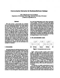
2. Miniature Embedded Reconfigurable Computer and Logic System The block diagram of the Miniature Embedded Reconfigurable Computer and Logic (MERCAL) module is shown in Figure 1. There are two primary components to the MERCAL module. They are the DIMM-PC and a Xilinx FPGA. The DIMM-PC is a commercially available, functionally complete, extremely compact (40 X 67 X 6 mm) PC motherboard containing either a 66 MHz 486SX or a 133 MHz AMD Elan SC586, onboard memory consisting of 16 to 32 Mbytes of RAM and a 16 to 32 Mbyte Flash Disk. The DIMM-PC peripheral interface consists of two serial
Printer Port Interface
DIMM PC
XILINX FPGA
PC Bus
I/O 81 pins
XC2S150-PQ208
Selected Signals
1. Introduction
disk controller ports. In MERCAL, the printer port is dedicated to the task of programming the Xilinx FPGA. Since this device is an SRAM based FPGA, it is possible, with software that has been developed, for the DIMM-PC to reconfigure the FPGA to satisfy the digital logic requirements for various applications. The FPGA used in MERCAL is the Xilinx XC2S150 Spartan-II in a PQ208 package. About half of the available I/O pins on the FPGA are used to interface to the DIMM-PC and the others are available external to the MERCAL module through connectors. The XC2S150 Spartan-II FPGA contains the equivalent of 150,000 gates with 200 MHz system performance. The interface to the MERCAL module provides 81 generalpurpose input output (IO) pins from the FPGA. The functions of these IO pins can be determined by the needs of the application and controlled by the configuration of the FPGA. Top and bottom views of the actual MERCAL module are also shown in Figure 1.
RS 232 Interface
This paper describes a design environment and platform developed to support senior capstone design projects in computer engineering that incorporates the concept of hardware/software codesign. A proposed capstone design project which utilizes this environment is also presented. This project is being undertaken by senior computer engineering students for the first time this year at the authors’ university.
32 MHz clock
Block Diagram
Top View
Bottom View
Figure 1. The Mercal Module
3. Hardware/Software Communications Library In order to assist the students in rapidly developing their project implementations, a library of standard hardware/software communications interfaces is being developed. Each interface contains a standard set of software procedures, developed in C which form an API for the particular interface. Using these routines, the user can send or receive data to/from the hardware across the interface and in some cases, configure or read the status of the interface. In the MERCAL system, these routines execute on the DIMM-PC when called by the application program. Each interface also contains a hardware module, written in synthesizable VHDL, that communicates with the software API routines across the
Proceedings of the 2003 IEEE International Conference on Microelectronic Systems Education (MSE’03) 0-7695-1973-3/03 $17.00 © 2003 IEEE
DIMM-PC/FPGA interface on the MERCAL. This hardware module resides in the Spartan FPGA and has a simple, well documented interface to which the user can interface the hardware portion of their application. The details of how the data is actually transferred across the DIMM-PC/FPGA interface is typically not of interest to the user unless they are planning on modifying the communications interface to better suit their application. Example interface types to be included in the library include: ● Memory mapped, non-blocking single word or block transfers ● Fully interlocked, blocking, single word or block transfers ● Variable depth FIFOs
As an example, consider the simple asynchronous memory mapped software-to-hardware data transfer interface. This interface is a simple method to transfer data from the software to the hardware without any synchronization mechanism whereby the software simply writes data to registers (memory) within the hardware. The data can be read by the hardware at any time and the values are whatever is stored in the memory when the hardware read takes place. The software interface to this data passing mechanism consists of one of two available procedure calls. The first interface procedure is called write_memory(char *data_array). The write_memory procedure takes a single argument that is a pointer to an array of characters that is the same number of bytes as the memory in the hardware. When this procedure is called, the software transfers the data from the location pointed to by the character pointer and transfers it to the hardware memory, one byte at a time. The second interface procedure is called write_memory_location(char data_value, char address). This procedure transfers a single byte of data to the specified address in the memory. On the hardware side, the interface is combinational in function. There is a Data output which is 8 bits, numbered (7 downto 0), and an Address input, which is Address_Size bits, numbered (Address_Size-1 downto 0). The Address input is used to address into the memory array. When a new address value is placed on the Address input, the data stored in that memory location is placed onto the Data output after an unspecified propagation delay. The delay between a new address value being placed on the Address input and the corresponding correct data value on the Data output must be determined from a post-synthesis timing simulation. There is an additional output from the memory to the hardware called Busy. The Busy output is asserted anytime that the hardware/ software interface is busy transferring new data into the memory. This output can be used by the hardware to determine if the values being read from the memory may be in the process of being updated and thus may be incorrect. A diagram of the hardware interface is shown in Figure 2.
In addition to the MERCAL, a version of the communications library for implementation on the Atmel FPSLIC [3] devices is being developed for those who may wish to use it but do not have access to a MERCAL platform.
4. Senior Capstone Design Project for 2003 - The Skybot A new project designed to utilize the capabilities of the MERCAL and the interface library has been developed. This project is based on the Skybot flying helicopter robot from Draganfly, Inc. The Skybot is a captive helicopter-like vehicle with two degrees of motion, up and down, controlled by the speed of its rotor, and clockwise and counter-clockwise rotation controlled by the tilt of the vehicle. The Skybot is shown in Figure 3.
Figure 3. The Skybot The goal of the project is to control the Skybot so that it can takeoff, pickup a metal ball from the ground using its built-in magnet, and deposit the ball in a designated area. This task will require the measurement of the vehicle’s position and velocity, and controlling of vehicle’s rotor speed, tilt motor, and electromagnet. This project involves the control of a more complex dynamic system then the robot project previously developed by the authors [2] and thus will provide a valuable testbed for the new hardware/ software environment being developed.
5. Acknowledgments The authors would like to thank Mentor Graphics Corporation for their donation of EDA tools, and technical support. This projects would not have been possible without their generous support. The authors would also like to acknowledge the National Science Foundation for their support of the development of the Codesign environment under CCLI Grant No. 0088688, and the NASA Langley Research Center for their support of the development of the MERCAL modules under Grant No. NAG-1-01042.
6. References Hardware
Memory
Data(7 downto 0)
Data from software
Address(Address_Size-1 downto 0) Busy
Figure 2. An example hardware interface
[1] Klenke, R. H., J. H. Aylor, “An Undergraduate Advanced Computer Design Course Using Virtual-Prototyping,” Proceedings of the IEEE Computer Society International Conference on Microelectronic Systems Education, July 1997, pp 62-63. [2] Klenke, R. H., “A Hardware/Software Codesign Senior Capstone Design Project in Computer Engineering,” Proceedings of the IEEE Computer Society International Conference on Microelectronic Systems Education, June 2001 pp. 58-59. [3] http://www.atmel.com/atmel/products/prod39.htm
Proceedings of the 2003 IEEE International Conference on Microelectronic Systems Education (MSE’03) 0-7695-1973-3/03 $17.00 © 2003 IEEE