TRANSACTION ON ELECTRICAL AND ELECTRONIC CIRCUITS AND SYSTEMS, VOL. 6(1), PP. 1-9, JAN., 2016.
A New Low Voltage Low Power Class AB Current Output Stage with High Current Drive Capability of 320mA Leila Safari
Abstract: This paper presents a novel low voltage low power class AB current output stage (COS) with high current drive capability. The proposed circuit is based on a novel control circuitry that eliminates channel length modulation effect of output branch transistors. Most remarkably the utilized control circuitry helps to reconcile the conflicting features of low voltage operation, low power consumption, high output impedance and high current drive capability altogether with simple structure and wide bandwidth. The approach is well suited for low voltage operation as it uses only two transistors between supply voltages at the output branch. Employing replica and current splitting transistors at the input branch along with the high gain current mirrors at the output branch enables the proposed COS to provide very high output currents under low supply voltages. The operation of the proposed COS is verified through HSPICE simulations based on TSMC 0.18µm CMOS technology parameters. Under supply voltage of ±0.9V, it can deliver large output current of 320mA with total harmonic distortion (THD) of -40.6dB. Of more interest is that the bias current of output branch transistors IB is only 73µA leading to the high current drive capability (Ioutmax/IB) of 4383. Its output impedance, current gain, -3dB bandwidth, power dissipation and chip area are also found as 1.57MΩ, 25.2dB, 4.63MHz, 156µW and 1.8mm×1.65mm respectively. Keywords: Current output stage, Current Mode, Current Mode Amplifier, High Current Drive Capability, High Output Current, Output Stage. 1
1.
INTRODUCTION
In recent years, low-voltage, low-power integrated circuit design has been receiving much momentum due to some strong motivations such as downscaling trend of integrated circuit technology and increasing demand for portable electronics [1-3]. Unfavorably as feature sizes decreased, the transistor gain factor gm.ro (with usual meaning of symbols) has also rapidly decreased and reaches to such dramatically low value of 3-6 in 65nm CMOS technology [4]. This problem along with other restrictions such as transistors large threshold voltage with respect to allowed supply voltages and their low output impedance preclude employment of classical analog circuits making it mandatory to find new solutions to preserve high performance of analog circuits. One of the new solutions is current mode signal processing Leila Safari is with Electrical and Electronics Faculty Iran University of Science and Technology (IUST), Electrical and Electronics Faculty/Electronics Research Center Iran University of Science and Technology (IUST), P.O. Box 16846-13114, Narmak, Tehran, Iran. (Email:
[email protected]).
which has been widely used to tackle the problems associated with analog circuit design owing to the potential advantages such as low voltage operation, wider dynamic range, simpler circuitry, wider bandwidth and lower consumed power [1-3, 5-14]. An essential part of current mode circuits is current output stage which plays a key role as the output stage of many current mode circuits among which are current feedback operational amplifiers (CFOA) and current mode operational amplifiers [10-14]. Many of the performance parameters of CFOA and COA such as linearity, output impedance and most importantly output current are directly determined by COS [10-14]. Therefore COS have attracted the attention of many authors [10- 14]. For high drive applications and off-chip loads, class AB COS is used. Compared to class A COS; in the class AB topologies signal amplitude to bias current can be increased resulting reduced power dissipation [14]. Fig.1 shows the conventional class AB COS [9]. It can be divided into three parts viz. bias part composed of M1-M3 transistors and current source IB, input transistors of M2, M4 and two simple current mirrors (CMs) composed of M5-M6 (for P-type CM) and M7-M8 (for N-type CM). Diode connected transistors M1, M3 along with IB current sources provide proper bias current for M2 and M4-M8 transistors. Input current applied to the input node is transferred to the output node by means of the aforementioned CMs. The complementary nature of the COS of Fig.1 (due to the use of both n-type and p-type current mirrors) allows it to deliver bipolar current to the output node.The performance of class AB COS is measured in terms of peak output current Ioutmax, drive capability i.e. Ioutmax/Ibias, linearity and output impedance. Unfavorably supply voltage reduction has made it very difficult to satisfy these varying features. Besides COS functions outside negative feedback loop and its performance is not enhanced by negative feedback action making the COS design task even more challengeable [14]. Actually, designers should try to reconcile several conflicting requirements such as high drive versus low voltage operation, low power dissipation versus wide bandwidth, high output impedance versus low voltage operation etc. To make these points clear, lets' consider two main limitaions of conventional COS of Fig.1: First; it requires large supply voltage to deliver large amount of Ioutmax. The main reason is large gate-source voltage required for the diode connected transistors M5 and M7 at high current levels. Fig.2 shows the required gate-source voltage of M5 for different input currents in 0.18µm TSMC technology. Curve (a), with transistors aspect ratio of 100µm/ 0.5µm shows the required gate-source
RECEIVED: 10, APR., 2015; REVISED: 12, JUN., 2015; ACCEPTED: 15, NOV., 2015; PUBLISHED: 4, JAN., 2016.
2
TRANSACTION ON ELECTRICAL AND ELECTRONIC CIRCUITS AND SYSTEMS, VOL. 6(1), PP. 1-9, JAN., 2016.
voltage of2V for input current of 10mA. Most warningly this voltage reaches to the extremely high value of 9.5V for input current of 80mA. Curve (b) is achieved by setting transistors aspect ratio to 1000µm/0.5µm. For such large aspect ratio, the required gate-source voltage of current mirror reduces to 1.8V for input current of 80mA. However the parasitic capacitance associated with such large size transistors degrades the frequency performance. Hence, in order to preserve frequency performance, bias current should be increased resulting in the decreased output impedance and increased power consumption. In brief trade off between bandwidth, output impedance, power dissipation and I outmax should be properly met. In [8], the required supply voltage of conventional COS of Fig.1 is reduced utilizing bootstrapped current mirror. Unfavorably the resulted COS suffers from low current drive capability due to the use of cascode structure at the output branch. The COS introduced in [14] which is shown in Fig.3, uses current splitting transistors of M6 and M8 to reduce the current of diode connected transistors and consequently their associated gate-source voltages. Therefore it makes possible to handle large amount of current under low supply voltages. The ratio of aspect ratio of splitting transistors to the diode connected ones determines the upper limit of Ioutmax. Employing the current splitting method, Ioutmax of ±24mA, under supply voltage of ±0.9V has been achieved in [14]. Under equal conditions, conventional one can deliver Ioutmax of only ±3.29mA [14]. Comparing the reported 24mA and 3.29mA, proves high potential of current splitting method in increasing the drive capability under low voltage restrictions.
complex and area inefficient because it uses a high gain OTA in negative feedback loop to boost the output impedance and increase linearity.
Fig.2. Input voltage of M5-M6 current mirror for different values of input current with transistors aspect ratios of a) 100µm/0.5µm b) 1000µm/0.5µm
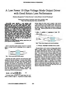
Fig.1. Conventional COS[9]
Second: It has low output impedance and poor linearity which is inherited from simple current mirrors used in its structure. The chanel length modulation effect of simple current mirrors adds significant amount of harmonic distortion to the output current. Under low supply voltage restrictions the sulotions based on cascode structures [8,10-13] such as dynamic matched and active gain enhanced current mirrors cannot be used to improve output impedance and linearity. Resistor based CMs utilized in [14] (Fig.3), enables very high output impedance and high linearity under low supply voltages. Unfavorably the COS of [14] is
Fig.3. Low voltage, high output current and high output impedance COS of [14]
A careful study shows that, among all previously reported works [8-14], only the COS of [14] provides the best parameters of large output current drive capability (Ioutmax/Ibias) and very large output impedance and is suited for low voltage low power applications. Particularly the COS of [14] is the only one with low input impedance resulted from the negative feedback loop established by current splitting transistors. However voltage drop across the used resistors in
TRANSACTION SERIES ON ENGINEERING SCIENCES AND TECHNOLOGIES (TSEST) ©
LEILA SAFARI.: A NEW LOW VOLTAGE LOW POWER CLASS AB CURRENT OUTPUT STAGE WITH HIGH CURRENT DRIVE CAPABILITY OF 320MA.
the input and output branches, is the main factor which limits the upper boundary of Ioutmaxin [14]. It also uses two high gain auxiliary amplifiers that increase the chip area, design complexity and degrades the frequency performance. Therefore in this paper a novel COS structure with extremely simple structure is proposed which exhibits a unique ultra large Ioutmax without sacrificing other desirable parameters such as low voltage-low power operation, high output impedance, high linearity and high frequency performance. To achieve large Ioutmax, the proposed COS, as a novelty, employs the current splitting loop along with replica input transistors to reduce the gate-source voltage of diode connected transistors as much as possible. Also to increase Ioutmax to maximum possible value, resistors and cascade structures are eliminated rather high linearity and high output impedance are maintained using two control circuitries composed of only four transistors. At the same time, the proposed control circuitries keep the drain-source voltage of output branch CM transistors equal resulting in high linearity and high output impedance. Unlike other previously reported works; in the proposed structure auxiliary amplifiers are not used. Therefore frequency performance, power dissipation and chip areas are optimized. There are also only two transistors at the output branch which enables the proposed COS to deliver maximum possible output current to the load. Of more intreset is the high current gain of the proposed COS which is beneficial in current mode building blocks such as COAs. Benefitng from high current gain, it can amplify low input current and deliver large amount of current to the load. This article is organized as follows: In section 2 the proposed COS is presented, simulation results are given in section 3 and finally section 4 conculds the paper.
2.
THE PROPOSED COS
connected transistors are the main reason of large supply voltage requirement of conventional COS of Fig.1 for driving large currents. In the proposed COS, a portion of input current is injected into the replica transistors M 5-M6, thus the current of M3-M4 transistors and those of M7, M9 are reduced properly resulting in their gate-source voltage reduction. In other words these transistors reduce the M 7 and M9 transistors’ share from the input current resulting in a significant reduction in their required gate-source voltage. To reduce the required gate-source voltage of diode connected transistors further, current splitting transistors M 8, M10 are also used. Detailed operation of current splitting method can be found in [14] however a brief explanation is given here. As it can be seen from Fig.4, drain terminal of splitting transistor M8 is connected to input node therefore input current injected into M3 is divided between M7and M8 transistors. Aspect ratio of M7 is K times larger than those of M8 i.e. (W/L)8=K.(W/L)7 thus drain current of M8 is K times larger than that of M7. Consequently large portion of input current is taken by M8 leaving a negligible portion to be sunk by M3 and M7. Thus the gate-source voltage of M7 is decreased to become able to handle larger (K times) amount of input currents. The similar explanation is held for lower half transistors (M4, M9-M10). The total required gate-source voltage of M7, M9 can be found as (with usual meaning of symbols): 𝑉𝐺𝑆7 = √ 𝛽
2×𝐼𝑖𝑛
𝑉𝐺𝑆9 = √ 𝛽
2×𝐼𝑖𝑛
7 (1+𝑥+𝑘)
9 (1+𝑥+𝑘)
A. Diode connected transistors gate-source voltage reduction technique: The first technique to reduce diode connected transistors M7, M9 gate-source voltage is using replica transistors M5-M6. As explained in the introduction section, diode
+ 𝑉𝑡7
(1)
+ 𝑉𝑡9
(2)
Where;
(𝑊⁄𝐿 ) (𝑊⁄ ) 8 = 𝑊 𝐿 10 (𝑊⁄𝐿 ) ( ⁄𝐿 ) 7 9 (𝑊⁄𝐿 ) (𝑊⁄𝐿 ) 5 6 = 𝑊 = 𝑊 ( ⁄𝐿 ) ( ⁄𝐿 ) 3 4 𝑊 = 𝜇𝐶0 𝐿
𝐾=
(3)
𝑥
(4)
𝛽
The conceptual schematic of the proposed COS is shown in Fig.4. It has some main differences compared to conventional COS of Fig.1 and COS of Fig.3 [14]: 1) Replica transistors M5-M6 are added parallel to the input transistors, 2) Current splitting transistors of M8 and M10are used. 4) Two control circuitries are added to the output CMs. Replica transistors and splitting transistors are used to reduce the required gate-source voltage of diode connected transistors of M7 and M9 and hence increase circuit’s drive capability. The control circuitries are used to reduce the channel length modulation effect of M12 and M14 transistors in order to increase output impedance and linearity. The detail operation of the proposed COS is described in two following subsections:
3
(5) As it can be seen from (1)-(2), for K, x>1, replica and splitting transistors play an important role in reducing gate-source voltage of M7 and M9 and making the proposed COS more capable to handle large amount of input currents under low supply voltages. The overall current gain can be found as: 𝐴𝑖 =
𝐼𝑜𝑢𝑡 𝐼𝑖𝑛
=
𝑥 1+𝑥+𝑘
×
(𝑊⁄𝐿)
12
(𝑊⁄𝐿)
=
11
𝑥 1+𝑥+𝑘
×
(𝑊⁄𝐿)
14
(𝑊⁄𝐿)
(6)
13
The input impedance can also be simply found as: 𝑅𝑖𝑛 =
1⁄ 𝑔𝑚3 1+𝐾
1⁄ 𝑔𝑚4
‖
1+𝐾
1
1
‖𝑔𝑚 ‖𝑔𝑚 5
(7) 6
B. Channel length modulation effect reduction technique: In the conventional COS of Fig.1, unequal drain-source voltages of mirroring transistors of M5-M6 at upper half and M7-M8 at lower half are the main reason of nonlinearity. However in the proposed COS, as another very effective innovation, drain-source voltage of mirroring transistors is kept equal using simple control circuitries. In other words channel length modulation effect of mirroring transistors is
TRANSACTION SERIES ON ENGINEERING SCIENCES AND TECHNOLOGIES (TSEST) ©
TRANSACTION ON ELECTRICAL AND ELECTRONIC CIRCUITS AND SYSTEMS, VOL. 6(1), PP. 1-9, JAN., 2016.
4
effectively reduced using control circuitries A and B shown in Fig.4. This not only improves the linearity of the proposed COS but also boosts its output impedance. Favorably there are only two transistors between supply rails at the output branch thus the proposed solution is well suited to low voltage applications. Implementation of control circuitries is shown in Fig.5 using only two transistors biased by related current sources and four transistors to implement the control circuitries. Despite such works as [10-14] which use high gain auxiliary amplifiers and have complex circuit thus suffer from degraded frequency performance, high level of noises and large power/area consumption, this circuitry, as another great innovation, is extremely simple hence breaks free from all those mentioned disadvantages. To explain the operation of the proposed control circuitries, without loss of generality we consider the lower half CM (Fig.4 and Fig.5-a) and assume that input current (Iin) is injected into the input node of the proposed COS (Fig.4) and then to the lower half through replica transistor M6. In the control circuitry A, M A1transfers output node voltage (drain voltage of M14) to the gate terminal of M A2. As MA2 has constant gate-source voltage (because it is biased with constant current source IB3), it acts as a voltage buffer and transfers the output voltage to the drain of M 13. Thus transistors MA1-MA2force the drain-source voltage of M13-M14to be equal. Now if output voltage decreases the drain-source voltages of M13will decrease simultaneously. According to the well known I-Characteristic of MOS transistors (with usual meaning of symbols):
due to non-zero value of λ, VDS reduction results in a reduced drain current of M13–M14. However the drain current of M13 is kept constant by input current and IB3 current source. Therefore gate voltage of M13 is increased by the feedback established by control circuitry A to compensate the reduction of drain current of M13 (due to its drain-source voltage reduction). Consequently the drain current reduction of M14 is also compensated due to the equal gate-source voltage of M13 and M14. Similarly when Vout increases, gate voltage of M13 is reduced to compensate any increase in the M13, M14 transistors drain current. Thus mirroring accuracy between M13 and M14 transistors are greatly improved and channel length modulation effect which is main concern in the design of COS, is effectively reduced.
VDD M7
M11
M8
M12
In-
out In+
(a)
Control Circuitry B
IB
M1
M3
M5 Iin
M4
M2
Iout
M6
IB Control Circuitry A In- out In+
M9
M10
M13
M14
VSS
(b)
Fig.4. Conceptual schematic of the proposed COS
ID
2
(V GS V th )2 (1 .V DS )
Fig.5. Implementation of a) A and b) B control circuitries
(8)
To derive the equations of output impedance, we start with the small signal equivalent circuit of Fig.5-a shown in
TRANSACTION SERIES ON ENGINEERING SCIENCES AND TECHNOLOGIES (TSEST) ©
LEILA SAFARI.: A NEW LOW VOLTAGE LOW POWER CLASS AB CURRENT OUTPUT STAGE WITH HIGH CURRENT DRIVE CAPABILITY OF 320MA.
Fig.6 in which α stands for the voltage transfer gain between MA1 gate and source (and is close to unity), gmi and gdsi denote the transconductance and output conductance of the related transistors respectively. The go A1 and goB2 also denotes the output conductance of M A1 transistor and IB3 current source respectively.
Using (15) and (16) total output impedance can be found as: 𝑅𝑜 = 𝑅𝑜𝑁 ‖𝑅𝑜𝑃 (17) To avoid negative output impedance, the following relations should be satisfied: 𝑔𝑜14 > 𝑔𝑜12 >
Fig.6. Lower half CM small signal equivalent circuit
Writing KCL at node (1) results: 𝑉𝑓 × 𝑔𝑜𝐵 + 𝑔𝑚𝐴2 (∝× 𝑉𝑜 − 𝑉2 ) + (𝑉𝑓 − 𝑉2 ) × 𝑔𝑜𝐴2 = 0 (9) or: 𝑔𝑚 +𝑔 ∝×𝑔𝑚𝐴2 𝑉𝑓 = 𝐴2 𝑜𝐴2 × 𝑉2 − × 𝑉𝑜 (10) 𝑔𝑜𝐵 +𝑔𝑜𝐴2
𝑔𝑜𝐵 +𝑔𝑜𝐴2
Writing KCL at node 2 gives: 𝑔𝑜13 × 𝑉2 + 𝑔𝑚13 × 𝑉𝑓 + 𝑔𝑜𝐵 × 𝑉𝑓 = 0 From Eq. (11), V2 can be written as:
(11)
𝑉2 = −
(12)
(𝑔𝑚13 +𝑔𝑜𝐵 ) 𝑔𝑜13
× 𝑉𝑓
By inserting (12) into (10) Vf can be found as: 𝛼×𝑔𝑜13 ×𝑔𝑚𝐴2 𝑉𝑓 = − × 𝑉𝑜
(13)
At output node we have: 𝐼𝑜 = 𝑔𝑚14 × 𝑉𝑓 + 𝑔𝑜14 × 𝑉𝑜
(14)
[𝑔𝑜13 ×(𝑔𝑜𝐵 +𝑔𝑜𝐴2 )+(𝑔𝑚13 +𝑔𝑜𝐵 )(𝑔𝑚𝐴2 +𝑔𝑜𝐴2 )]
Substituting Eq. (13) into Eq.(14) , the output impedance of lower half current mirror (RON) can be found as: 𝑅𝑂𝑁 = [𝑔𝑜14 −
𝛼×𝑔𝑜13 ×𝑔𝑚𝐴2 ×𝑔𝑚14
−1
] (15)
[𝑔𝑜13 ×(𝑔𝑜𝐵 +𝑔𝑜𝐴2 )+(𝑔𝑚13 +𝑔𝑜𝐵 )(𝑔𝑚𝐴2 +𝑔𝑜𝐴2 )]
From (15), it can be seen that the effect of finite output impedance of M14 (i.e. non zero value of go14) is reduced significantly. Similarly, the upper half output impedance can be written as: 𝑅𝑂𝑃 = [𝑔𝑜12 −
𝛼′ ×𝑔𝑜11 ×𝑔𝑚𝐵2 ×𝑔𝑚12
−1
]
[𝑔𝑜11 ×(𝑔𝑜𝐵 +𝑔𝑜𝐵2 )+(𝑔𝑚11 +𝑔𝑜𝐵 ′ )(𝑔𝑚𝐵2 +𝑔𝑜𝐵2 )]
(16) Where α’, goB’ and gmB2 are the voltage gain between gate and source of MB1, output impedance of IB4 and transcounductance of MB2 respectively.
5
𝛼×𝑔𝑜13 ×𝑔𝑚𝐴2 ×𝑔𝑚14 [𝑔𝑜13 ×(𝑔𝑜𝐵 +𝑔𝑜𝐴2 )+(𝑔𝑚13 +𝑔𝑜𝐵 )(𝑔𝑚𝐴2 +𝑔𝑜𝐴2 )] 𝛼′ ×𝑔𝑜11 ×𝑔𝑚𝐵2 ×𝑔𝑚12 [𝑔𝑜11 ×(𝑔𝑜𝐵 +𝑔𝑜𝐵2 )+(𝑔𝑚11 +𝑔𝑜𝐵 ′ )(𝑔𝑚𝐵2 +𝑔𝑜𝐵2 )]
(18)
(19)
Complete implementation of the proposed COS is shown in Fig.7. LS1 and LS2 are simple level shifters required for proper biasing of MA1 and MB1respectively. The implementation of LS1 and LS2 is shown in Fig.8.In order to reduce bias current of output branch (and increase the output impedance, a current source Ion equal to IB3 can be added between the source of MA2 and Vss in the lower half. Similarly another current source (Iop) equal to I B6 can be added between source of MB2 and VDD. Ion and Iop are not shown in Fig.7 for simplicity. To maintain the stability of negative feedback loop established by MA2, M13 in the lower half and MB2, M11 in the upper half compensation capacitors may be required which can be added between gate-drain of M11 and M13.
3.
SIMULATION RESULTS
The proposed COS of Fig.7 and the conventional one of Fig.1 are simulated in equal condition with HSPICE using 0.18µm TSMC CMOS process parameters under supply voltage of ±0.9V. The transistors aspect ratios and the values of used element are reported in table 1 and table 2 respectively. Two capacitors of 1pF and 1.3pF between gate and drain terminals of MB2 and MA2 are used respectively for stability. The frequency performance of the proposed COS is drawn in Fig.9.The DC gain and -3dB bandwidth of the proposed COS is 25.2dB and 4.63MHz respectively. In equal conditions, the conventional COS shows -3dB bandwidth of only 0.131MHz.Compared to the COS of [14] and conventional COS of Fig.1, the -3dB bandwidth of the proposed COS is improved by a factor of 46.3 and 32 times respectively. The frequency performance of the proposed structure can be enhanced further by increasing bias current of transistors at the expense of increased power dissipation and reduced output impedance. The power dissipation of the proposed COS is measured as 156µW which make it suitable for low power applications. It exhibits high output impedance of 1.57MΩ. Actually the output node of COS is usually connected to a low value load; therefore 1.57MΩoutput impedance is enough to preserve good accuracy. On the other hand without control circuitries, the output impedance is only 32.43KΩ. Consequently, control circuitries boost the output impedance by a factor of 48.
TRANSACTION SERIES ON ENGINEERING SCIENCES AND TECHNOLOGIES (TSEST) ©
6
TRANSACTION ON ELECTRICAL AND ELECTRONIC CIRCUITS AND SYSTEMS, VOL. 6(1), PP. 1-9, JAN., 2016.
Fig.9. Frequency performance of the proposed COS
Fig.10. DC transfer characteristic of the proposed COS
Fig.7. implementation of the proposed COS
The DC transfer characteristic of the proposed current output stage for grounded load is shown in Fig. 10. As the outstanding property of the proposed COS, it can deliver output currents as high as 320mA with THD of -40.6dB while the bias current of output branch transistors is only 73µA leading to the extremely high current drive capability of 4383, the largest reported value so far.
Fig.8. Implementation of level Shifters
Fig.11-a shows THD variation for different values of peak amplitude of output current evaluated for 1KHz sinosoidal input. As it can be seen, THD remaind below -30dB. To investigate THD variation with mismatches, Monte Carlo simulation is carried out by considering 3% mismatch in VTH and Tox of all transistors in 30 runs and applying sinusoidal input with 1KHz frequency. The amplitude of Iout is set to maximum value of 320mA. The resulted THD variation is shown in Fig.11-b which proves the robustness of the proposed COS against process variations. Figure 12 shows the step response of the proposed COS for maximum output current namely 320mA which proves the good stability of the proposed COS. The power supply rejection ratio (PSRR) of the proposed COS is also examined. It shows 108dB and 107dB of PSRR+ and PSRR- respectively. The layout of the proposed COS is shown in Fig.13. All the requirements have been considered to avoide electron migration and to reduce parasitic capacitances and resistances[15]. It occupies an area of 1.8mm*1.65mm. Although large size output transistors at the output branch produce very large parasitic capacitanes around 30pF, but the large parasitic capacitances of their drain and source terminals have not significant effect on the frequency performance. Thanks to the uniqe structure of the proposed COS, the drain and source nodes of large sized transistors at the output branch are connected to low value load and supply rails respectively. Therefore they don't play an important role on the frequency performance. The post simulaton results
TRANSACTION SERIES ON ENGINEERING SCIENCES AND TECHNOLOGIES (TSEST) ©
LEILA SAFARI.: A NEW LOW VOLTAGE LOW POWER CLASS AB CURRENT OUTPUT STAGE WITH HIGH CURRENT DRIVE CAPABILITY OF 320MA.
7
shows a -3dB bandwidth of 3.68MHz. The resulted reduction in the bandwidth is due to the effect of parasitic capacitances of M3-M11 and M13 transistors.
(a)
Fig.13. The layout of the proposed COS
(b) Fig.11. a) THD variation for different valuse of output currents b) Histoghram of THD in the presence of 3%Mismatches for the proposed COS.
The results are compared with those of conventional COS and some other class AB current output stages in Table-3. As can be seen, the proposed COS exhibits the ultra high Ioutmax, while preseves its high frequency performance. It is the only reported COS structure which provides current gain larger than unity.This property helps to increase the peak output current. However it also results in the reduced output impedance and increased power dissipation due to the increased bias current of output branch transistors.
TABLE 1. TRANSISTORS ASPECT RATIOS AND ELEMENT VALUES
Transistors
Aspect Ratio(µm/µm)
Transistors
Aspect Ratio(µm/µm)
M1,M3 M2,M4 M5 M6 M7 M8 M9 M10 M11
036/0.36 72/0.72 72/.36 144/0.72 90/0.18 900/0.18 36/0.9 360/0.36 72/0.72
M12 M13 M14 MA1 MA2 MB1 MB2 MLS1 MLS1
15840/0.72 144/0.72 15840/0.36 0.72/0.36 11.8/0.54 2.52/0.36 0.36/0.9 36/0.36 3.6/0.18
TABLE 2. THE USED ELEMENT VALUES
Elements
Fig. 12. Transient response of the proposed COS
IB1,IB2 IB3,IB4,IB5,IB6, IB8 IB9
4.
Value 0.2µA 0.1µA 10µA 5µA
CONCLUTION
In this paper a new COS structure is presented that breaks free from the disadvantages of all previously reported ones in terms of low frequency performance, low current gain, complicated circuit. Benefiting from two simple control circuitirs, it provides high current drive capability, high TRANSACTION SERIES ON ENGINEERING SCIENCES AND TECHNOLOGIES (TSEST) ©
TRANSACTION ON ELECTRICAL AND ELECTRONIC CIRCUITS AND SYSTEMS, VOL. 6(1), PP. 1-9, JAN., 2016.
8
linearity, high gain , wide bandwidth and high output impedance. Instead of using complicated axuilary amplifiers, it takes advantages of a simple control circuity consisting of only two transistors. Eliminating the high gain axuillary amplifiers, grant the proposed COS very simple structure. In brief the proposed COS introduces some novel and effective ideas to resolve the problems associated with previously reported works. Implementing the proposed structure in older technologies in which the supply voltage is very large compared to VTH of transistors will increase Ioutmax further at the expense of reduced refrequency performance due to low fT of transistors in older technologies. Besides using expensive low threshold technologies, the proposed COS can provide even larger Ioutmax.
REFERENCES [1] E. Yuce, S. Minaei: A First-Order Fully Cascadable Current-Mode Universal Filter Composed of Dual Output CCIIs and a Grounded Capacitor. Journal of Circuit Systems and Computers, 2016, DOI: 10.1142/S0218126616500420. [2] E. Yuce, S. Minaei: Realization of arbitrary current transfer functions based on commercially available CCII + s. International Journal of Circuit Theory and Applications , DOI: 10.1002/cta.1880. [3] L. A. Said, A.H. Madian, M.H. Ismail, A.M. Soliman: Current Feedback Operational Amplifier (CFOA) Based Programmable Lossless Floating Inductor Realization. 2014, DOI: 10.1109/ICEngTechnol.2014.7016778. [4] X. Zhao, H. Fang, J. Xu:DC gain Enhancement method for recycling folded cascode amplifiers in deep submicron technology. IEICE Electronics Express,
Vol.8, (2011), pp.1450-1454. [5] L. Safari, S.J. Azhari: A Novel Wide Band Super Transistor Based Voltage Feedback Current Amplifier. Int.J.Electron.Commun.(AEU), Vol. 67, (2013), pp.624-631. [6] N. Herencsar, A. Lahiri, K. Vrba, J. Koton:An electronically tunable current-mode quadrature oscillator using PCAs. Int. J. Electronics, Vol. 99, (2012), pp. 609–621. [7] G. Ferri, N. Guerrini: Low-Voltage Low-Power CMOS Current Conveyors. Kluwer Academic Publishers, Boston (2003). [8] G. Palmisano, G. Palumbo, S. Pennisi: Solutions for CMOS Current Amplifiers with High Drive Output Stages. IEEE Transactions on Circuits and Systems-II, Analog and Digital Signal Processing, Vol. 47, (2000), pp.988-998. [9] E. Bruun: Worst Case Estimate of Mismatch Induced Distortion in Complementary CMOS Current Mirrors. Electronics Letters,Vol. 34, (1998) , pp.625-27. [10] G. Palmisano, G.Palumbo, S.Pennisi: High Linearity CMOS Current Output Stage. Electronics Letters,Vol. 31, (1995), pp.789 – 790. [11] G.Palmisano, G. Palumbo, S.Pennisi: Harmonic Distortion on Class AB CMOS Current Output Stages. IEEE Transactions on Circuits and Systems-II: Analog and Digital Signal Processing,Vol. 45, (1998), pp.243-250. [12] G.Palumbo, S. Pennisi: Low-voltage class AB CMOS current output stage. Electronics Letters, Vol.35 , (1999), pp. 1329-1330. [13] A.Zeki, H. Kuntman: High-Linearity Low-Voltage Self-Cascode Class AB CMOS Current Output Stage. IEEE International Symposium on Circuits and Systems, Vol.4, 2000, pp.257-260.
TABLE 3. COMPARATIVE PARAMETERS OF THE PROPOSED COS AND OTHER WORKS
Refs. Supply voltage(V) Gain(dB) **IB(µA) Maximum Iout(mA) Ioutmax/IB
[10] NA 0 100 NA 30
[11] NA 0 100 NA 30
[12] 2 0 1.5 0.13 86.6
[13]1 2.5 0 3 0.1 33.33
[13]2 2.5 0 3 0.1 33.33
[14] ±0.9 0 7.5 24 3200
Proposed ±0.9 25.2 73 320 4383
Rout(MΩ)
NA
NA
2200
21.5
5130
350
1.57
-3dB Bandwidth (MHz)
NA
NA
35
6.63
28.7