impedance matching terminators is presented. Finally a novel Adaptive Multi-Level Simultaneous bi-directional. Transceiver (AMLST) bus structure for cache or ...
A Novel Memory Bus Driver/Receiver Architecture for Higher Throughput Gregory E. Beers and Lizy K. John Department of Electrical and Computer Engineering The University of Texas at Austin Austin, TX 78712 {beers, ljohn}@ece.utexas.edu
Abstract A high-speed memory bus interface which enables greater throughput for data reads and writes is described in this paper. Current mode CMOS logic synthesis methods are used to implement multi-valued logic (MVL) functions to create a high bandwidth bus. First, a fundamental bi-directional data bus for multiple logic levels is presented. Then a bi-directional data bus with impedance matching terminators is presented. Finally a novel Adaptive Multi-Level Simultaneous bi-directional Transceiver (AMLST) bus structure for cache or main memory is proposed. The proposed bus can balance the memory channel bandwidth with the instruction execution rate of modern processors. Despite the problems encountered in implementing complete systems with MVL circuits, among which are circuit speed and design automation support, there is great potential in the future for this approach.*
1. Introduction As processor cycle times continue to decrease, it is becoming more difficult for memory systems to keep instructions and data streams flowing at the processor execution rate. This has resulted in a serious speed disparity between processors and memories. The main goal for improving the memory design is to maximize memory channel throughput by minimizing the latency and increasing bandwidth. System architectural improvements like Synchronous DRAMs (SDRAMs) [Sdr97] memory interface have been used in many systems to increase the bandwidth. In some recent research Saulsbury et al. [Sau96] discusses the “memory wall” and proposed to break down the wall by integrating *
This work was supported in part by the National Science Foundation under grant CCR-9697098.
large amounts of memory into the chip along side the processor. This would allow wide fast bus structures to be designed between the processor and memory. This solution is elegant but for one thing, dynamic memory technology is still not directly compatible with processor technology. They are converging though, with 5-levels of metal versus 3-levels for DRAM, but they are just not there yet. And then there are the test issues and commodity pricing issues. Until there is an identical process designed to integrate both memory and DRAM without restricting the processor design due to process limitations, there is a need for high speed off chip buses and driver/receiver designs. In this paper, we propose a novel Adaptive MultiLevel Simultaneous bi-directional Transceiver (AMLST) bus structure for connecting processors to off-chip caches or main memory. Multi-Valued Logic (MVL) circuits have been shown in the past to reduce chip area, power consumption, and interconnect wiring in certain applications versus their fully binary alternative. The proposed multi-valued logic bus can balance the memory channel bandwidth with the instruction execution rate of modern processors. The paper also describes the multivalued logic bi-directional data bus patented in US patents [Bee96a, Bee96b]. This paper is organized as follows. In section 2, we describe the past research in computer design using MVL. In section 3, the proposed memory bus interface design is presented. In section 4, the proposed bus driver/receiver circuit is compared with other existing bus interfaces. In section 5, we summarize the paper and offer some concluding remarks.
2. Related Research Madsen et al. [Mad95] describes high-speed crossbar switch interconnects for processor to processor communication using ternary logic (3-Level Logic). As a prelude to the proposed design, a fast and accurate circuit
will guarantee low skew data so that the additional levels available may be used for data transfer thus reducing the I/O count or increasing the bandwidth for the same number of I/Os. If the system noise is low enough to allow more levels than required for the data on the bus any additional levels can be used to implement some form of self-clocking circuitry. Also with the increasing clock frequencies of the future board designs, rigorous transmission line design and analysis will need to be performed. More MVL circuit design is discussed in [Cur92] using CML (current mode logic) which is described as a hybrid of binary logic and analog signal processing. There are definite theoretical advantages to using MVL logic; mainly the reduction of interconnection complexity due to the higher information content per wire. In addition power savings are possible. When CML is used the current source circuit can be designed to be independent of power supply variations. In order to take full advantage of the MVL design approach all subsystems should be designed using this technique. The memory cells would now contain more informational density since they are comprised of multiple levels. The transfer of information from the memory onto the data bus now would not require a conversion from multi-level to a binary logic level. K.W. Current [Cur95] describes a memory circuit that uses MVL to store information which could be used for cache and register design for a savings of silicon real estate. Memory can also be designed using MVL as proposed in [Lee95] where 4-valued memory experimental devices were shown to work. Dynamic current mode memory was proposed in [Lee92] using MVL circuits. Since more levels of storage in a single cell degrade noise margins, error correction techniques were applied to overcome this problem. This is similar to the proposed bus implementation technique where the dynamic level adjustment with bandwidth demand may reduce noise margins so some form of ECC (Error Correction Code) is require to guarantee fault-tolerance. It is interesting to note that in [Lee92] the memory cells were designed using current mode instead of voltage mode logic to enhance speed. The applications for memory devices range from high-speed cache memory, data and tag, to application specific memories. The most recent trend is to buffer DRAMs then clock out the data synchronously with a well timed circuits that have low or adjusted system skew. The more familiar names for these types of RAMs are termed SSRAM (Synchronous Static RAM) and SDRAM (Synchronous DRAM). In addition the RAMBUS design provides for a word wide specialized high-speed synchronous terminated bus designed for high throughput.
3. Proposed Memory Bus Interface Design In order to increase the throughput of the memory channel a higher bandwidth topology is proposed. The design is based on the idea that more than one bit of information can be transmitted on a single signal line of the data bus if multiple levels are used. This in itself is not a new idea but the implementation or method is. Current mode CMOS logic synthesis methods [Bar92] are used to implement multiple valued logic (MVL) functions as will be needed to create the proposed high bandwidth bus. Current levels are used instead of voltage to improve upon the sensitivity of the circuits to power supply variations. These variations are a source of degradation in signal-to-noise ratios. There are still many other sources of signal disturbance that will be mentioned further into the paper. Figure 1 shows the basic topology of a bi-directional data bus, which could be used for any type of I/O channel, memory. It consists of a transmitter device and a receiving device at both ends on a transmission line. This topology for a data bus is termed point-to-point due to the fact that there are only two pairs of transmitters/receivers on the bus. The proposed design topology is restricted to this type of bus design and will become clear further into the paper. This type of data bus configuration can be used for multiple levels of data information transmission and reception. Figure 1. Fundamental Bi-directional Data Bus for Multiple Logic Levels
The number of multiple logic levels (Ln) is described as: 2 ≤ Ln ≤ N, where, N = maximum levels. The value N is determined by: 1) the requested bandwidth, 2) the system noise, 3) the system configuration, and 4) the number of levels of ECC and parity available. N is also adaptable to provide peak rates that vary depending on the above changes in parameters during system operation. Now figure 2 expands the level of detail to include a bi-directional data bus with termination. In order for the digital signal to be detected at the receiving end with the maximum integrity there must be a transmission line impedance matching device which is called a terminator. This is shown as Zt in the diagram. Also shown
symbolically is a current source driver for sending the signal current down the transmission line along with a high input impedance MOSFET receiver circuit. Figure 2. Bi-directional Data Bus Diagram with Termination
If the current source driver depicted in figure 2 was made to be able to handle more that one level of current then the circuit would be transformed into a multiple level transmitter. Along with this idea observe the signal drawings shown in figure 3. Here there are more than two logic levels, three to be exact. This now allows signals to be sent from both ends of the transmission line at the same time since the transmission line acts linearly and the currents follow the superposition theorem. If a transmitting device knows what is being sent from its end this signal can be given to receiver logic to be subtracted from the measured input signal to derive the true received signal. This decoding takes place in parallel with the transmission of the data. In the design topology shown in figure 3, the bus signaling can accommodate a Write + Read transaction overlap in addition to transmitting multiple levels in any one direction. Figure 3. Simultaneous Bi-directional Signal Levels
A design for a Multi-level Simultaneous Bidirectional Data Bus was proposed in [Bee96a, Bee96b] which utilized current mode multilevel transmission of digital data. Receive and transmit operations could be performed simultaneously over a single bus thus increasing bandwidth and reducing the arbitration and
control logic complexity. Although this is a benefit there is a decoding penalty that must be addressed if the entire processor is not based on MVL design. This means a conversion somewhere in the data path must be made to obtain binary levels from tertiary levels. In the following paragraphs, an Adaptive Multi-Level Simultaneous Transceiver (AMLST) is proposed. This circuit dynamically changes the number of logic levels (current levels for AMLST) transmitted and received for maximum throughput. Figure 4 shows the topology required to implement the AMLST. For brevity only one side of the bus interface is shown. The current source driver is depicted in the “io” block. This type of current source driver is described in detail in [Bee96a, Bee96b]. The driver injects a multi-level current signal into the transmission line, which is propagated to the receiver in the other chip. It should be noticed that the current is split between the active termination device and the transmission line, although at the receiving end the current will terminate in a like termination device. The CML (Current Mode Logic) receiver circuit detects the many levels of current and sends them to the MVL decoder/encoder block. Figure 4. Concept Drawing for AMLST Processor / Memory Bus Interface
The “io” block (Current Source Driver Circuit): The current source driver consists of a PMOS circuit driver with speedup predrivers as described in [Bee96a, Bee96b]. This circuit provides voltage compliance to the power supply rail in order to tolerate varying power supply conditions, DC voltage and AC transients. The output impedance of this current source device is designed to be high in relation to the active termination device so that its effect on termination will be minimal.
Practically there will be a large variation in the PMOS current driver output impedance with varying power supply voltage and load voltage levels. The CML (Current Mode Logic) receiver circuit: involves multiple differential current comparators to detect the signal levels. The basic CML receiver circuit design is described in more detail in [Bee96a, Bee96b]. Transmission Line interconnect: This is comprised of a standard point-to-point connected micro-strip or stripline interconnect with a nominal characteristic impedance of 65 ohms in a FR-4 multilayer printed circuit board. Active Termination Device: The basic circuit is comprised of an NMOS FET effectively connected in an active load configuration with the gate controlled by the drain. One implementation of this device is described in [Bee96a, Bee96b]. The device is scaled such that the dynamic impedance is nominally at the transmission line impedance for the driver current levels used. Dynamic Termination Control: The active termination device, which is controlled by the MVL decode/encode circuit block, can be adjusted to optimize the device impedance for different current levels. Since the device impedance curve is non-linear a controlling circuit is used to compensate for the non-linearities associated with changes in current levels. This can be accomplished by switching in multiple FET terminator devices in parallel depending on the current levels expected. That would provide for a closer match of the termination device to the characteristic impedance providing optimization of the transmission line reflection characteristics. Current Reference Circuit: In order to accurately detect the transmitted current levels across the transmission line interface it is necessary to exchange current references between integrated circuit modules. The reference circuit is used for compensation of the various circuit devices for process, temperature, and voltage changes. This allows a more robust design making it possible to interconnect differing technologies since the current values are tightly controlled by a precise reference such as a band-gap device. Also designing with low voltage drivers/receivers allows for a wider range of power supply voltage tolerances. There is usually only one current reference interconnect per chip, but there is no restriction on the number of references that can be used. In fact a particular design might use a one-per-byte ratio although the advantage of fewer I/O pins is diminished. Practically certain designs might require additional references above one-per-chip as in: a high number of drivers, extreme noise conditions, multiple wide buses required, a reference per bus due to different driver types, on chip variations across the die, or more current levels required than the noise tolerance will permit.
Noise Level Detection Circuit: In order to dynamically adjust the number of current levels for varying conditions a noise level circuit is required. Several sources of noise are monitored and adjusted for. Among these sources are: Vdd noise along with its associated droop, ground bounce, clock noise, random noise, and non-correlated but periodic noise. Depending on the level of sophistication and expected noise environment a sampling of inputs could be measured for crosstalk and transmission line reflected noise. In order to accomplish this, quiet line receivers need to be implemented. These could be dedicated lines or time shared. Also depending on the complexity allowed in design, the quiet lines could be selected sequentially or at random with their data being encoded with other driver circuits. This could be accomplished since multi-levels are employed. It must be noted though that both interconnected chips must be synchronized and be in cooperation for this level of sophistication. Dynamic Adapter Logic: This is mainly comprised of decision logic. Based on the noise detection inputs and the dynamic ECC requirements control signals are sent to the MVL decoder/encoder block to set up the number of levels transmitted. ECC Control Logic: This block has requirements beyond the standard error detection, correction, and control function. It must also be able to dynamically adjust the amount of correction based on the number of levels transmitted and received. For added fault-tolerance in the face of system noise two circuit blocks are added: 1) a noise level detection circuit and 2) an ECC (Error Correction and Control) logic circuit. These two circuit blocks feed a dynamic adapter logic circuit that will change the available valid logic levels, N, based on system parameters. Other sensitivity parameters may be used to determine N, which could include a process variation sensing circuit, an aging circuit, and a power supply level detector circuit. Initialization Logic: A required control block not shown in figure 4 but described here for completeness is an initialization circuit. In order to initialize or reset the driver circuit the inter-chip reference circuits must communicate between each other at start up to determine the characteristic impedance for the interconnecting data bus. Adjustments are performed to set up the dynamic termination at the beginning of power on or reset phase. Multi-Valued Logic Decoder/Encoder Circuit: The MVL Decoder/Encoder circuit is the heart of the driver/receiver controller logic. It is here where received data and transmitted data are compared in order to extract the received signal. In addition to the driver and receiver data signals, control inputs and outputs connect other logic blocks. Specifically the dynamic adapter logic
instructs the controller on the maximum number of levels that may be reliably transmitted. It should be emphasized that in a homogenous design where all circuits internal and external are implemented with MVL the decode/encode block is unnecessary since signals remain in MVL.
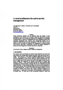
4. Comparison with other Bus Interfaces Table 1 lists a fairly complete set of driver/receiver technologies. Figure 5 charts the driver voltage swings along with the noise margins for the various driver/receiver technologies. The chart coarsely plots the newer technologies going from the left to the right. What is important to note is that the newer designs are trending toward lower voltage swings. This output voltage swing reduction is due to several factors which are: 1) the lower available power supply voltage, 2) the requirement for faster rise and fall times (at fixed voltage slew rates, lower delta voltages yield shorter time delays) and, 3) lower electromagnetic radiation. Also of interest is the fact that more emphasis is placed on noise level as a percentage of the signal swing. Observe that the old technology TTL had a poor signal-to-noise ratio while a new technology, GTL or Gunning Transistor Logic maintains almost a 2:1 ratio, although the absolute value of the noise is approximately the same. CMOS, although a mature technology is the exception to the rule since it maintains a good 2:1 ratio. That is one of many reasons why it is the dominant technology of the present day. The right end pair of bars show the AMLST estimated signal swing and noise margin for the proposed driver design for N equal to 2. The AMLST circuits are designed to provide both a low voltage output swing and a optimal noise margin. Figure 5. Comparison of AMLST with other bus driver/receiver technologies
Bus Signaling Comparisons
4 3 2 1
S TT L LV TT L R SL BT L C TT H ST L G T AM L LS T
O M
C LV
M
O
S
0
C
Voltage (V)
5
Noise Margin Voltage swing
Driver Type
AMLST has the following advantages: 1. 2. 3. 4. 5. 6. 7.
More bits per transfer Variable peak rates designed to match demands Error correction features built in for reliability Adaptable signaling in the presence of noise Graceful degradation due to noise tolerance Fewer I/O required for same bandwidth Internally active transmission line termination at Zo (characteristic impedance)
The disadvantages of AMLST are the following: 1. New circuit technology 2. Lack of support from design automation tools 3. A mixed signal design approach is required 4. Transmission line analysis required for best performance 5. For best utilization requires both MVL memory and processor designs 6. For adaptability closer integration with CPU required Some of the important design considerations and requirements include the number of levels, N being high or increasing which translates to a higher probability of bit errors with a given noise margin. For increasing N: 1. ECC bits increase 2. Transmission Line analysis is required 3. Tighter tolerance on chip-to-chip references 4. Retry capability is required at some N threshold 5. Scheduling of send and receive data during quite system times 6. Skew the data clock to different sub-buses for lower noise
5. Summary and Concluding Remarks In this paper, we presented a novel memory bus interface design for higher data throughput. Multi-valued logic (MVL) principles were used to design the high throughput bus. A bi-directional data bus using MVL, a bi-directional MVL data bus with impedance matching terminators, and an Adaptive Multi-Level Simultaneous bi-directional Tranceiver (AMLST) bus structure were presented. The various building blocks constituting the AMLST bus structure were described in detail. The AMLST design can be utilized in high performance systems from a system architectural point of view where the CPU-centric and the memory-centric issues are in balance. Despite the problems encountered in implementing complete systems with MVL circuits, among which are circuit speed and design automation
support, there is great potential in the future for this approach.
References [Bar92]
M. H. Abd-El-Barr and M. I. Mahroos, “On the Synthesis of MVL Functions for Current-Mode CMOS Circuits Implementation”, Proceedings of the 22th International Symposium on MultipleValued Logic, pp. 221-228, 1992. [Bee96a] G. E. Beers, R. E. Frankeny, and M. M. Smadi, “Bidirectional Transmission Line Driver/Receiver”, United States Patent No. 5,568,064, Oct. 22, 1996. [Bee96b] G. E. Beers, R. E. Frankeny, and M. M. Smadi, “Bidirectional Transmission Line Driver/Receiver”, United States Patent No. 5,578,939, Nov. 26, 1996. [Cur92] K. W. Current, “A Current-Mode CMOS Algorithmic Analog-to-Quaternary Converter Circuit”, Proceedings of the 22nd International Symposium on Multiple-Valued Logic, pp. 229-234, 1992. [Cur95] K. W. Current, “Memory Circuits for Multiple Valued Logic Voltage Signals”, Proceedings of the 25th International Symposium on Multiple-Valued Logic, pp. 52-57, 1995.
[Han95] T. Hanyu, A. Mochizuki, and M. KameyamaMultipleValued Arithmetic Integrated Circuits Based on 1.5V Supply Dual-Rail Source-Coupled logic”, Proceedings of the 25th International Symposium on Multiple-Valued Logic, pp. 64-69, 1995. [Sdr97] IBM Microelectronics Web site, “Synchronous DRAMs: The DRAM of the Future”, http://www.chips.ibm.com/products/memory/sdramart /sdramart.html. [Lee95] C. L. Lee, H. N. Chern, M. S. Liao, and H. M. Wang, “On Designing of 4-Valued Memory with DoubleGate TFT”, Proceedings of the 25th International Symposium on Multiple-Valued Logic, pp. 187-192, 1995. [Lee92] E. K. F. Lee and P. G. Gulak, “Dynamic CurrentMode Multi-Valued MOS Memory with Error Correction”, Proceedings of the 22th International Symposium on Multiple-Valued Logic, pp. 208-215, 1992. [Mad95] J. K. Madsen and S. I. Long, “A High-Speed Interconnect Network using Ternary Logic”, Proceedings of the 25th International Symposium on Multiple-Valued Logic, pp. 2-7, 1995. [Sau96] A. Saulsbury, F. Pong, A. Nowatzyk, “Missing the Memory Wall: the Case for Processor/Memory Integration”, ISCA ‘96, pp. 90-101, May 96.
Table 1. Digital Bus Interface Comparison of Types I/O TYPE TTL ECL HSTL LVTTL CMOS LVCMOS GTL CTT BTL RSL Rambus AMLST AMLST
Voh
Vol
Vih
Vil
2.4 -0.96 1.1 2.4 Vdd-0.2 Vdd-0.1 1.2 1.9 2.1 3.1 Vt+(Io*Zo) Vt +(Io*Zo)
0.4 -1.65 0.4 0.4 0.2 0.1 0.4 1.1 1.1 1.5 Ib * Zo Ib * Zo
2.0 -1.105 1.85 2.0 0.7Vdd 2.0 0.85 1.7 1.62 2.65 Vt + Io*Zo Vt + Io*Zo
0.8 -1.475 0.65 0.8 0.2Vdd 0.8 0.75 1.3 1.47 0.95 Ib * Zo Ib * Zo
Vnoise_margin High/Low 0.4/0.4 0.1/0.15 0.25/0.25 0.4/0.4 Vdd/2-0.2 Vdd/2-0.1 0.35/0.35 0.2/0.2 0.48/0.37 0.45/0.45 0.5 *(Io-Ib)*Zo 0.25*(Io-Ib)*Zo
Vpp Swing 2.0 0.8 0.7 2.0 Vdd-0.4 Vdd-0.2 0.8 0.8 1.0 1.15 (Io-Ib)* Zo (Io-Ib)* Zo
Vt, Rt, Vref Termination na parallel 50 ohms to Vt= -2.0 na series Zo-Rs series Zo-Rs 50 ohm Vtt=1.2 Vth=1.55 1.9