... networks, high-perfor- mance computing, remote memory access, device virtual- ..... plete network suitable to support cluster computing. As host interface the ...
A resource optimized remote-memory-access architecture for low-latency communication Mondrian Nüssle
Martin Scherer
Ulrich Brüning
Computer Architecture Group University of Heidelberg Germany {mondrian.nuessle, martin.scherer, ulrich.bruening}@ziti.uni-heidelberg.de ABSTRACT This paper introduces a new highly optimized architecture for remote memory access (RMA). RMA, using put and get operations, is a one-sided communication function which amongst others is important in current and upcoming Partitioned Global Address Space (PGAS) systems. In this work, a virtualized hardware unit is described which is resource optimized, exhibits high overlap, processor offload and very good latency characteristics. To start an RMA operation a single HyperTransport packet caused by one CPU instruction is sufficient, thus reducing latency to an absolute minimum. In addition to the basic architecture an implementation in FPGA technology is presented together with an evaluation of the target ASIC-implementation. The current system can sustain more than 4.9 million transactions per second on the FPGA and exhibits an end-to-end latency of 1.2 µs for an 8-byte put operation. Both values are limited by the FPGA technology used for the prototype implementation. An estimation of the performance reachable on ASIC technology suggests that application to application latencies of less than 500 ns are feasible. Keywords: interconnection networks, high-performance computing, remote memory access, device virtualization
1. Introduction High-performance-computing today is a synonym for parallel computing. Efficient communication functions between nodes of a distributed memory machine are a key component for such architectures. A number of commodity hardware functions exist to address the communication between such machines. The scalability of applications as well as the applicability of new paradigms of development and implementation, especially the PGAS [1] methodol-
ogy, can be increased or enabled by very low-latency interconnect systems. PGAS systems based on intermediate libraries like GasNet [2] or zero-copy MPI [3] implementations can benefit from efficient remote memory access architectures that provide hardware support for put and get operations. In this work a resource optimized, remote memory access architecture is introduced, which exhibits very low latency and high computation-communication overlap. It will be shown that the architecture would provide for unprecedented performance if implemented in ASIC technology. An important design choice for the RMA engine is the use of HyperTransport [4] technology to interface the device hardware with the host processor and main memory. This interface allows for a connection between device and host with the lowest latency. A study of the latency characteristics of PCI-Express 1.1 [5] implementations available for different FPGA technologies showed that the latency of the PCI-Express connection alone equals the complete endto-end latency reached on the RMA prototype including software layers, NIC, switching and network link layer. The RMA unit described in this paper can be complemented with the Virtualized Engine for Low Overhead (VELO [6]) to form a NIC with additional features for high-performance computing. The combination is especially appealing since VELO shares some of the on-chip infrastructure with RMA. VELO is optimized to transmit small messages in a send/receive style using main-memory ring-buffers on the receiving side, while RMA can be used to transport larger MPI messages, MPI-2 [7] one-sided communication and put/get operations in PGAS style models. The primary contribution of this paper is the architecture of an extremely optimized unit for remote memory access that exhibits unique characteristics in terms of latency, low-overhead, and virtualization. The hardware architecture also allows for a very flexible notification sys-
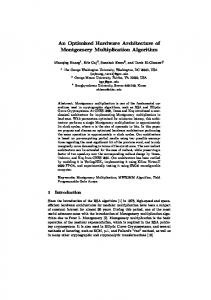
2. Hardware architecture The RMA unit is divided into three sub units, the Requester, the Completer and the Responder. Figure 1 gives an overview of the three sub-units, the host interface using an on-chip interconnection network named HTAX crossbar and the network layer using the network port modules. Every command passes the Requester unit on the sending path. If the command is a get style command, it is transmitted to the Responder on the remote side, which generates the necessary response to be sent back to the original sender. Finally, every command is completed in the Completer unit, which usually writes the result into main memory. In a modern multi-core machine a number of processes or threads need efficient concurrent access to the network. A virtualized network controller function is a hardware unit, that although it is present only once in hardware, can be simultaneously used by different processes at the same time. A necessary condition for this scenario is that cores submitting an operation to the device must do so in an atomic manner. Otherwise, commands from different processes may get intermingled with each other leading to erroneous behavior. At the same time, it is essential to avoid main memory accesses and to optimize the submission of new operations to the device. For a low-latency
To / From Host
HTAX Crosbar
RMA Units
tem which can be leveraged to implement various protocols on top of the basic hardware in a very efficient way. For example, the possibility of notifying the target of a completed operation allows for efficient implementation of two-sided, zero-copy protocols on top of the native hardware operations. The RMA unit implements a virtualized device meaning that the hardware engine can be used by a number of user processes simultaneously and the engine is able to handle all the aspects including the security requirements that are associated with the use-case of the device. A dedicated hardware unit, the Address Translation Unit (ATU), deals with the secure exchange of memory references between user processes and hardware. The RMA hardware architecture is implemented using FPGA technology. The resulting design together with the necessary software layers is evaluated in a complete system which yielded very encouraging results. The rest of this paper is organized as follows. In the next section the architecture of the hardware is introduced. In Section 3 the software stack used to interact with the hardware is presented. An evaluation of the FPGA implementation follows using a number of different microbenchmarks and a short analysis of the performance reachable on ASIC technology. Finally, a comparison of the RMA architecture with related work is provided in Section 5.
RMA Requester
RMA Completer
Network Port
RMA Responder
Network Port To / From Network
Figure 1. RMA Units device it is also necessary to avoid kernel interaction, i.e. the device must be able to employ user-level communication techniques. By implementing a single, shared command queue for all contexts, the amount of on-chip memory for this queue compared to one queue per context is minimized. Reverseflow-control features, that are present in the HyperTransport link, which connects the device to the host, are used to prevent queue overflow. To enable the atomic insertion of new queue elements, the commands are of a fixed and limited size. One command is specified by a 9 bit op-code, the ID of the destination and source process, the destination node ID and a 128-bit data item specifying command dependent operands, usually the source and destination memory address as well as the data count of the operation. The limited size of the command is carefully chosen, so that the complete command can be written to the device using a single MOVNTDQ [8] command, which is atomic in the AMD Opteron architecture. This operation is followed by a serializing SFENCE instruction to flush the write combining and write buffers of the CPU. The op-code, the process IDs and the destination node ID are handled through information that is embedded within the requester address. The requester address is the offset within the device’s memory mapped physical base address region (BAR). The use is comparable in many ways to the method employed by the VELO unit [6]. As one can see in Figure 2, high-order bits encode the destination node within the network and lower-order bits the destination context on that node. The size of these fields can be changed to fit the number of nodes in the network and the number of desired contexts within each node. Three bits are used to enable signaling of remote management access, notification via interrupts and disabling of address translation. All of these bits reside beyond the page boundary, so it is possible for supervisory software to
Page boundary Higher address part selects page
Target Node (m bit)
Target VPID (n bit)
Source VPID (n bit) Management bit
Page
Cmd. Notif. (3 bit) (3 bit)
Reserved (6 bit)
Interrupt Enable Bit AT enable bit
Figure 2. Requester Addresses restrict user processes to communicate only with certain peer processes. The interrupt bit, if set, triggers an interrupt on the respective node whenever a notification is written to main memory. It can be used to implement asynchronous messaging, for example for in-kernel protocols like remote storage applications. The address translation bit is turned off by kernel level agents using the RMA unit to prevent address translation of source and destination addresses. Finally, the management bit allows access to configuration and status registers of a remote node, so management software running on one node is able to configure and monitor the whole network using RMA transactions. Within the page boundary another set of information is encoded: the command and the notification enable bits. Via the command bits, the user application can specify the operation that is to be performed. Currently seven different operations are defined. These are put and get operations with a word granularity and a cache line granularity supporting single operations with a maximum size of 4 kilobyte. Besides these basic operations, the immediate put operation can be used to transport a 64-bit value embedded into the command to a specified location in remote memory. The notification put operation transports a 64-bit value as well as an additional 8-bit value into a notification entry at the remote side. This operation is especially useful for the implementation of synchronization, management and control purposes. Finally, the remote atomic operation can be used for synchronization purposes, for example to natively implement the full MPI-2 lock and unlock semantics. There are three notification enable bits which act as an additional qualifier to every command. Each bit designates whether a notification entry is to be generated at the corresponding unit. In other words, a get operation can optionally generate a notification when it passes the requester unit, when it passes the responder unit and when it passes the completer unit. For put style operations the responder notification bit is ignored. Notifications are 128-bit entries that are written into a ring buffer in main memory. There is one notification queue per user context. Notifications record source and destination of an operation, the actual op-code and a memory address (or data in the case of a notification put). This notification scheme is simple, efficient and very flexible at the same time. Classic one-sided
RMA solutions do not provide for a notification or completion at the passive side of an operation. Hence, it is sometimes difficult for upper layer protocols to detect the completion of a data transfer operation. The flexible notification system of the RMA unit can help to implement a wide variety of upper layer protocols elegantly on top of RMA operations. The maximum size of an RMA operation is 4 kilobyte as mentioned above. Together with the restriction that the source or destination memory region of an operation is not allowed to pass a page boundary, it is guaranteed, that only a single address translation per operation is necessary. Since starting a single operation is very cheap, larger transactions that pass a page boundary have to be formed by successively posting messages with a maximum size of 4 kilobyte each. Section 5 of this paper will also present measurements that demonstrate the high rate of operations that can be posted from a single core supporting this claim. Address translation is an integral part of every userspace device that directly interacts with arbitrary virtual memory on commodity, standard operating systems. Devices generally need to address the host’s main memory using physical addresses, while user applications only know virtual addresses. The problem has been solved in this architecture using a dedicated hardware unit called Address Translation Unit (ATU). All RMA sub-units are able to communicate with the ATU through the on-chip HTAX interconnection crossbar. The units are sending requests containing the virtual address information to the ATU, which responds with the corresponding physical address. The virtual addresses used by the ATU are called Network Logical Addresses (NLA). They form an additional virtual address space with a page granularity of 4 kilobytes, which is independent from the virtual address space of the operating system. This enables the implementation of a low latency address translation mechanism that is optimized for the use in remote memory access environments. Physical addresses are fetched from the translation table in the main memory or from the integrated translation lookaside buffer (TLB), which is part of the ATU. When the address information is not stored in the TLB, only one main memory access is needed to receive the physical address. The unit is able to maintain address translation for all processes using the RMA engine.
3. Software Architecture The software stack, that has been implemented to use the RMA hardware, is shown in Figure 3. Four kernel modules manage the hardware. The base driver manages the PCI device (since a HyperTransport device is seen as a PCI device from software). On top of the base driver, there is one driver for the ATU, one for the RMA unit and one
Host Interface
Application
NIC
User-Application
Network Linkport
ATU
VELO
Middleware, i.e. MPI, GasNET (Library)
User Space
HyperTransport IP Core
Networkport
HTAX XBar
Linkport
Networkport
Linkport Network XBar
RMA Networkport
rmadrv
Base Driver
PCI Configspace
RMA
Kernel bypass
libRMA
atudr v
registerfile Kernel Space
C&S Registerfile
Linkport
Linkport
Linkport
Figure 4. Block Diagram
ATU
Registerfile
NIC
Network Hardware
Figure 3. RMA Software Stack driver to access and manage the control and status register file. The library offers functions, such as rma_register and rma_unregister for memory management, and functions to put or get remote memory. On top of librma, other middleware libraries can be layered which implement industry standard interfaces for applications. Two examples are MPI and GasNET. Currently, two components for OpenMPI [9] which implement MPI-1 [3] respectively MPI-2 [7] onesided functionality are already being tested.
4. Evaluation The architecture has been prototyped on a Xilinx Virtex4 FPGA [10]. The FPGA is mounted on the HTXBoard [11] together with other components forming a complete network suitable to support cluster computing. As host interface the low latency HyperTransport [4] interface was selected. It is implemented by the HT-Core [12], an open source HyperTransport IP. A block diagram of the complete architecture is shown in Figure 4. The design can be roughly divided into three parts, the host interface (on the left side), the network interface controller (NIC, middle) and the network block (on the right side). The host interface block is formed by the HT-Core and the on-chip HTAX crossbar which connects the functional units with the host interface and with each other. The different functional units for communication as well as the supporting modules, like ATU and a control and status registerfile, are located in the NIC block. Here, the
VELO [6] engine is added to the design as an additional functional unit to complement the characteristics of the RMA unit. Contrary to most network interface designs, this architecture contains the complete logic for a network switch on-chip. The transport and link layer that is implemented by the network hardware features six bidirectional, serial links with hardware retransmission and a crossbar switch. The physical transport is realized using the MGT transceivers of the FPGA [13], optical SFP transceivers and optical cabling. The network employs virtual-cutthrough routing, virtual channels to enable deadlock-free minimal routing in 3-D torus topologies, a flit size of 64 byte and a data path width of 16+2 bit. The implementation of this architecture on a Virtex4 FX100 FPGA uses about 95% of the available slices. On a speed grade 12 device, we were able to reach 180 MHz clock speed for all parts except the HT-Core, which is clocked at 200 MHz. We believe that this constitutes a good result for an FPGA implementation. From the 180 MHz and the datapath width of 16 bit follows, that each link can sustain a unidirectional 360 MB/s raw link bandwidth. After subtracting the resources used up for 8b/10b coding, framing, CRC and routing, 88% of the raw link bandwidth is available to payload. The aggregated bandwidth of the integrated switch is 3.24 GB/s. Memory registration latency. For the performance evaluation of the RMA and ATU units, their particular lowlevel software interfaces were used. The first benchmark shows the latency caused by the registration and deregistration of main memory pages for the use with the RMA hardware. The results of the measurement done on a real system have been plotted in Figure 5. For reference, the measurement was also repeated using a Mellanox ConnectX Infiniband HCA [14]. These results are very encouraging; and they show that the time to (de-)register memory is dominated by the linear time it takes to perform a software table
2.5
150
2
Latency [ns]
registration latency in usec
200
100
1.5
1
50 0.5
Notification Put Immediate Put without notification Immediate Put with notification Put without notification Put Get Remote Lock
0 0
500
1000
1500
2000
registration size in kilobytes ATU Registration ATU Deregistration Mellanox Connect X Registration Mellanox Connect X Deregistration
Figure 5. Memory (De-)Registration Latency walk to translate the user virtual to a physical address. In comparison to other network adapters, the ATU allows a much faster (de-)registration of memory; the measured time for one page stays below 2 µs in both cases. On a Mellanox Connect X adapter an average latency of ~50 µs was measured for the registration of a small number of pages. The deregistration process on ConnectX hardware also took ~50 µs. The graph shows a considerable amount of jitter and peaks which are probably caused by background processes and Linux memory management. The exact causes remain to be investigated, though. These results are in line with other studies of memory registration performance [15]. We believe that a low registration/deregistration latency can help to leverage the architecture’s possibilities in a higher variety of use cases. This is confirmed by a large number of publications dealing with the optimization of the registration process by investigating caching [16][17][18] or buffer re-use [19][20]. Latency and bandwidth. The next experiment explored the latencies for a representative subset of operations supported by the RMA unit (minimum sized transactions, application to application latency). The result of this experiment is given in Figure 6. The measurement very nicely shows the impact that additional DMA transfers have on the latency, considering the difference between an immediate put with or without notification. All latencies are half round-trip, except the remote lock and the get transactions, where a full-round-trip was measured since this forms the integral latency of the operation. The experiment as well as the following measurements was performed on two machines with dual Opteron 870 (2.0 GHz) and 4 GB of memory each. All measurements include software overhead, CPU and caching effects as well as the network latency including two passes through a switch and the substantial delay introduced by the Xilinx MGT SerDes imple-
0
Figure 6. Latencies of RMA Operations mentation. In summary, the network contributes about 450 ns to the complete latency. Using an immediate put operation, a half round-trip latency of 1.2 µs for 8 bytes of payload could be reached. Next, ping-pong latency and streaming bandwidth of put and get operations of various sizes were measured. The results are shown in Figure 7 and Figure 8. In both cases, the horizontal line shows the maximum reachable bandwidth which can be sustained by the link after subtracting the overhead for framing, routing and CRC. The measurements show, that RMA is easily able to reach full bandwidth, but much more importantly, the curves all exhibit a sharp slope. Thus, even small transactions can call on a high bandwidth. Message rate and overlap. Other important characteristics of a communication unit are the message rate and the amount of overlap between computation and communication. The architecture presented here performs nearly ideally in this regard. The start of an operation is not much more than some preparation followed by a 128-bit SSE2 store operation. Further processing of the transactions is completely offloaded from the CPU. Measurements show that on average more than 4.9 million operations per second can be issued by a single CPU core. Efficient usage of message passing protocols is based on the ability of overlapping communication and computation. To assess the performance of the RMA unit in this respect, an experiment was conducted where the prototype of the MPI-2 onesided implementation was used to measure the amount of overlap that can be reached on the architecture. The method used to analyze overlap is based on the experiments described in [21] where the authors implemented an improved method for overlapping communication and computation on Infiniband hardware and evaluated the impact using a specially developed microbenchmark. A similar code was executed on the RMA unit. The results of this experiment are shown in Figure 9. A synchronizing function followed by an MPI_Put with varying sizes and again a synchronizing function form the basis of this test. In addition, an increasing amount of computation is per-
7
350
RMA Put RMA Get Bandwidth [MB/s]
8
Latency [us]
6 5 4 3 2
300 250 200 150
RMA Put RMA Get Peak payload bandwidth Half peak payload bandwidth
100 50
1 0 10
100
1000
Size [byte], logarithmic scale
Figure 7. Ping-Pong Latencies formed within this region. The relative amount of computation in percent was measured that can be added to the synchronized region without increasing the overall time it takes to complete the region. The results show, that the RMA unit is able to support high overlap even for small transaction. ASIC estimation. Finally, the architecture was analyzed in respect to an ASIC implementation. Early synthesis and place and route results for a current standard cell ASIC flow (65 nm) show, that the design is able to reach more than 800 MHz clock frequency. Figure 10 shows the latency and bandwidth characteristics of the MPI-2 OSU put benchmark [22], when using different implementation technologies. This benchmark integrates MPI-2 synchronization overhead in addition to the raw put latency. The current FPGA prototype reaches a latency of 2900 ns while the Mellanox ConnectX QDR Infiniband HCA reaches 2576 ns (albeit in a faster host system with 2.83 GHz CPUs). At 800 MHz core frequency and using an HT1000 HyperTransport interface, the low-level latency is calculated to be 500 ns and the OSU put latency to be 1200 ns. At the same time the uni-directional payload bandwidth is estimated to reach in excess of 2.8 GB/s. For this calculation a 32-bit wide internal data path was assumed, since the area constraints of the FPGA implementation no longer apply. An additional implementation choice would be to use 64-bit data paths doubling the bandwidth.
5. Related Work In the past, high performance network implementations have strived for low latency and high message rates. The Martini chip [23] is an interesting research project as well as ATOLL [24][25]. Further networks include Myrinet [26], Quadrics QsNet II [27] and other cluster interconnects. All of them generally employ user-level communication, a certain level of endpoint virtualization and support for virtual memory in remote memory operations. Myrinet
10
100
1000
Size [byte], logarithmic scale
Figure 8. Streaming Bandwidth MX [28] for example does not support one-sided operations, while Quadrics can operate directly on virtual memory using a Linux kernel patch. All these networks do not implement a streamlined architecture for optimal latency and message rate characteristics as the one described here. In recent years Infiniband [29] based interconnection networks have seen increasing interest in the high-performance and parallel computing communities. The current hardware generation from Mellanox, the Connect X HCA [14] exhibits very good latencies and can reach very high bandwidth. In [30] the write latency between two hosts using OpenFabrics is reported to be 1.8 µs for 128 bytes. The Infiniband adapters are also virtualized devices that offer 512 contexts, memory registration possibilities, twosided and one-sided communication primitives. The difference to the work presented in this document is two-fold: first of all the architecture presented here can reach comparable latencies although the prototype hardware has to cope with the significant performance penalty of being implemented in a FPGA rather than an ASIC. In their study Kuon et al. [31] showed that the difference in reachable clock speeds between an FPGA implementation and an ASIC is anywhere between 3-5 times. The evaluation of an ASIC version of the RMA architecture supports this study. Secondly, the architecture presented here performs better for small messages, shows a much higher message rate normalized to the link bandwidth and performs much better in areas such as memory registration and deregistration, which are often not covered in micro benchmarks but nevertheless are important for application speed. One especially interesting approach is described in an article from K.D. Underwood et al [32]. The authors present a network architecture that is based on the Seastar design [33] used in recent Cray supercomputers. In many ways this work is similar to the work described here. It is also a HyperTransport based network which aims for lowlatency and high message-rate throughput. There are a number of differences, though. First of all the architecture is less optimized. It does not implement a true cut-through
size [bytes] MPI_Fence MPI_Lock, exclusive
MPI_Lock, shared MPI_post/wait/start/complete
Figure 9. MPI-2 overlap architecture as the RMA unit described here. For example, descriptors have to be written completely to an on-chip buffer, before the actual hardware processing of the transfer can begin. And, even more importantly, descriptors are of a bigger and variable size than the largest integral data type of the CPU, thus requiring more than one PIO transaction to trigger the network operation. The approach described in this work minimizes descriptors in such a way that they can be posted using one single CPU store operation thus reaching the optimum for posting a network descriptor. Also, in [32] the NIC hardware is neither virtualized, nor can it handle virtual addresses in the way commodity operating systems manage the memory of a machine. Both are not necessary for a network device which is envisioned to be used in a closed environment supercomputer architecture as the Cray XT [34] family. Finally, the authors describe a fairly high-level simulation of the approximate behavior of such an architecture, while the architecture described here is evaluated in a complete prototype system.
6. Conclusion In this paper a new architecture for Remote Memory Access has been described. The major contributions of this work are an optimized, virtualized hardware function for remote memory access. This function is optimized for lowlatency and high communication/computation overlap. The architecture takes advantage of the advanced features of HyperTransport and modern CPUs and is thus able to reduce the overhead to start and complete a communication operation to the minimum. The simplest immediate put operation requires only one 128-bit store on the sender side, while the payload is written to the receiver memory with a single memory transaction. The average put case needs one additional memory access from the device, to fetch the data from the main memory of the sender. The
3500
3500
3000
3000
2500
2500
2000
2000
1500
1500
1000
1000
500
500
0
Latency [ns]
Bandwidth [MB/s] 6
8
51 2 10 24 20 48 40 96 81 92 16 38 4
25
12
64
32
overlap [percent]
100% 90% 80% 70% 60% 50% 40% 30% 20% 10% 0%
0 Reference: Mellanox ConnectX QDR IB OSU put latency [ns]
ASIC, FPGA, HT1000, HT400, 800 MHz, est. 180 MHz usable bandwidth [MB/s]
Figure 10. Technology effects on MPI-2 Put Performance virtualization and state minimization techniques employed enable a hardware function that supports multiple, virtualized endpoints in an FPGA device. Also, the RMA uses a novel area and speed optimized address translation unit (ATU) introduced to work securely in a user-space communication environment. In the related work section it was shown how this method corresponds to other work in the area of computer architecture and interconnection networks. Finally, we show a complete system implementation of the architecture together with microbenchmark performance measurements. The results are very promising and, as far as we know, the best results for such a network on FPGA basis ever published.
7. References [1] K. Yelick, D. Bonachea, W. Chen, P. Colella, K. Datta, J. Duell, S. L. Graham, P. Hargrove, P. Hilfinger, P. Husbands, C. Iancu, A Kamil, R. Nishtala, J. Su, M. Welcome, T. Wen. Productivity and performance using partitioned global address space languages, Proc. of the 2007 International Workshop on Parallel Symbolic Computation, London, Canada, July 2007. [2] D. Bonachea. GASNet specification, v1.1, Technical Report UCB/CSD-02-1207, U.C. Berkeley, October 2002. [3] Message Passing Interface Forum. MPI: A Message-Passing Interface Standard Version 1.3, 2008, http://www.mpi-forum.org/docs/docs.html, visited Sept. 2008. [4] HyperTransport Technology Forum. HyperTransport™ I/O Link Specification, Revision 3.00c, www.hypertransport.org, 2007. [5] PCI-SIG. PCI Express Base Specification, Rev. 1.0, 2002. [6] H. Litz, H. Froening, M. Nuessle, U. Bruening. VELO: A Novel Engine for Ultra-low Latency Message Transfers, Proc. of the 37th International Conference on Parallel Processing (ICPP-08), Portland, Oregon, September 2008.
[7] Message Passing Interface Forum. MPI-2: Extensions to the Message-Passing Interface, http://www.mpi-forum.org/docs/mpi2-report.pdf, 2003, visited August 2008. [8] Advanced Micro Devices, Inc. AMD64 Architecture Programmer’s Manual Volume 1: Application Programming, Publication No. 24592, Revision 3.14, September 2007. [9] E. Gabriel, G. E. Fagg, G. Bosilca, T. Angskun, J. J. Dongarra, J. M. Squyres, V. Sahay, P. Kambadur, B. Barrett, A. Lumsdaine, R. H. Castain, D. J. Daniel, R. L. Graham, T. S. Woodall. Open MPI: Goals, Concept, and Design of a Next Generation MPI Implementation, Proc. of the 11th European PVM/MPI Users' Group Meeting (Euro-PVM/MPI04), Budapest, Hungary, 2004. [10] Xilinx, Inc. Virtex-4 FPGA User Guide, UG070 (v2.6) December 1, 2008. [11] H. Fröning, M. Nüssle, D. Slogsnat, H. Litz, U. Brüning. The HTX-Board: A Rapid Prototyping Station, Proc. of the 3rd annual FPGAworld Conference, Stockholm, Sweden, Nov. 2006 [12] D, Slogsnat, A. Giese, M. Nüssle, U. Brüning. An OpenSource HyperTransport Core, ACM Transactions on Reconfigurable Technology and Systems (TRETS), Vol. 1, Issue 3, p. 1-21, Sept. 2008. [13] Xilinx, Inc. Virtex-4 RocketIO Multi-Gigabit Transceiver User Guide, UG076 (v4.1) November 2, 2008. [14] Mellanox Technologies. ConnectX Architecture, http://www.mellanox.com/content/pages.php?pg=products_dyn&product_family=39&menu_secti on=40, visited February 2009. [15] F. Mietke, R. Rex, R. Baumgartl, T. Mehlan, T. Hoefler, W. Rehm. Analysis of the Memory Registration Process in the Mellanox Infiniband Software Stack, European Conference on Parallel Computing (EURO-PAR), Dresden, Germany, Aug. 2006. [16] L. Ou, X. He, J. Han. A Fast Read/Write Process to Reduce RDMA Communication Latency, Proc. of the 2006 International Workshop on Networking, Architecture, and Storages, Shenyang, China, Aug. 2006. [17] T. S. Woodall, G. M. Shipman, G. Bosilca, A. B. Maccabe. High Performance RDMA Protocols in HPC, Proc. of the 13th European PVM/MPI Users' Group Meeting (Euro PVM/MPI 2006), Bonn, Germany, Sept. 2006. [18] F. Mietke, R. Rex, T. Mehlan, T. Hoefler, W. Rehm. Reducing the Impact of memory registration Infiniband, 1. Workshop Kommunikation in Clusterrechnern und Clusterverbundsystemen (KiCC), Chemnitz, Germany, Nov. 2005. [19] J. Liu, B. Chandrasekaran, J. Wu, W. Jiang, S. Kini, W. Yu, D. Buntinas, P. Wyckoff, D. K. Panda. Performance Comparison of MPI Implementations over Infiniband, Myrinet and Quadrics, Proc. of the International Conference on Supercomputing (SC’03), Phoenix, USA, 2003. [20] M. J. Rashti, A. Afsahi. 10-Gigabit iWARP Ethernet: Comparative Performance Analysis with InfiniBand and Myrinet10G, IEEE International Parallel and Distributed Processing Symposium, Long Beach, USA, March 2007.
[21] G. Santhanaraman, S. Narravula, D. K. Panda. Designing passive synchronization for MPI-2 one-sided communication to maximize overlap, IEEE International Symposium on Parallel and Distributed Processing IPDPS, Miami, USA, 2008 [22] OMB package, http://mvapich.cse.ohio-state.edu/benchmarks; visited February 2009. [23] K. Watanabe, T. Otsuka, J. Tsuchiya, H. Nishi, J. Yamamoto, N. Tanabe, T. Kudoh, and H. Amano. Martini: A Network Interface Controller Chip for High Performance Computing with Distributed PCs, IEEE Transactions on Parallel and Distributed Systems, Volume 18, Issue 9, 2007. [24] U. Brüning, L. Schaelicke. ATOLL: A High- Performance Communication Device for Parallel Systems, Proc. of the 1997 Conference on Advances in Parallel and Distributed Computing, Shanghai, China, March 1997. [25] H. Fröning, M. Nüssle, D. Slogsnat, P. R. Haspel, U. Brüning. Performance Evaluation of the ATOLL Interconnec, IASTED Conference, Parallel and Distributed Computing and Networks (PDCN), Innsbruck, Austria, February 2005. [26] N. J. Boden, D. Cohen, R. E. Felderman, A. E. Kulawik, C. L. Seitz, J. N. Seizovic, W. Su. Myrinet: A Gigabit-per second Local Area Network, IEEE Micro, 15(1):29-36, 1995. [27] F. Petrini, W. Feng, A. Hoisie, S. Coll, E. Frachtenberg. The Quadrics Network: High-Performance Clustering Technology, IEEE Micro, Volume 22, Issue 1, 2002. [28] Myricom Inc. Myrinet Express (MX): A High-Performance, Low-Level Message-Passing Interface for Myrinet, version. 1.2. 2006. [29] Infiniband Trade Association. InfiniBand Architecture Specification Volume 1, Release 1.1, 2002. [30] S. Sur, M. J. Koop, L. Chai, D. K. Panda. Performance Analysis and Evaluation of Mellanox ConnectX InfiniBand Architecture with Multi-Core Platforms, High-Performance Interconnects, 2007. HOTI 2007. 15th Annual IEEE Symposium, August 2007 [31] I. Kuon, J. Rose. Measuring the gap between FPGAs and ASICs, Proc. of the 14th international Symposium on Field Programmable Gate Arrays, Monterey, USA, Feb. 2006. [32] K. D. Underwood, M. J. Levenhagen, and R. Brightwell. Evaluating NIC Hardware Requirements to Achieve High Message Rate PGAS Support on Multi-Core Processors, International Conference for High Performance Computing, Networking, Storage, and Analysis (SC'07), Reno, Nevada, November 2007. [33] R. Brightwell, K. T. Predretti, K. D. Underwood, T. Hudson. SeaStar Interconnect: Balanced Bandwidth for Scalable Performance, In IEEE Micro, 26(3):41-57, May-June 2006. [34] Cray Inc. Cray XT. http://www.cray.com/products/XT.asp, visited February 2009.