A Performance Driven Layout Compaction Optimization Algorithm for Analog Circuits Henry H. Y. Chan and Zeljko Zilic
Department of Electrical and Computer Engineering McGill University, Montreal, PQ H3A 2A7 Email:
[email protected],
[email protected] Abstract -- In interconnect-dominated designs, the ability to minimize layout-induced parasitic effects is crucial for rapid design closure. Deep sub-micron effects and ubiquitous interference in mixed-signal environments cause designers to be less reliant on optimization based solely on schematic models. Performance can be further improved at the physical design level. Hierarchical optimization schemes are used to manage the complexity in the analog circuit design process. In this paper, we present a novel performance-driven compaction optimization algorithm that optimizes the placement of circuit blocks and guard bands for analog circuits. Parasitic effects are minimized under symmetry, matching and displacement constraints derived from the customized layout topology. I. INTRODUCTION High demands of quality electronic devices have driven the interests in rapid design and development of robust mixed-signal integrated circuits using deep-submicron (DSM) technologies. A key concern for DSM design closure is the parasitic coupling through the interconnect, packaging and substrate parasitics, due to nonideal electrical isolations. Under the shortened design cycle times, efficient physical design techniques and accurate parasitic coupling models are needed in overcoming signal integrity issues, achieving the desired quality and productivity. Due to the regenerative nature of digital signals, automated physical design generation tools have long been effective in synthesizing digital hardware subsystems. Meanwhile, analog components are still largely crafted from bottom-up. To keep pace with logic design, top-down design flow is urgently needed [1]. Unless with overly pessimistic specifications, robustness at the top abstraction level against interference such as substrate coupling and routing parasitics is not guaranteed until the detailed physical design information is extracted. To improve design closure, a hierarchical optimization scheme that continually refines design options throughout the top-down design flow is suggested (Fig. 1). In this paper, we propose a performance-driven, simulation based compaction optimization technique, where the designer supplies a physical design and its exact block and guard band locations are optimized. Based on the given layout topology for CMOS bulk substrate process, cost functions in terms of interconnect and substrate coupling parasitics are minimized while subjected to block symmetry, matching and displacement constraints. The algorithm explores possible reductions of performance impact due to layout effects with no change in existing schematic and physical design topology. Placement is a critical step in the physical design flow to ensure satisfactory performance, because layout parasitics and routability are strongly dependent on quality physical placement. Placement algorithms can be separated into 2 major classes: partitioningbased and simulation-based algorithms. Partitioning algorithms divide the complex problem repeatedly into smaller, more manageable sub-problems. Within each level, the geometric partitioning is optimized with respect to objective functions, using a predetermined partition style. Partitioning-based algorithms are more suitable for large circuits where global exploration of placement possibilities cannot be performed efficiently. In simulation-based algorithms, randomly or evolutionarily generated trial placements are carried out. Performance or resource related cost functions are
1-4244-0921-7/07 $25.00 © 2007 IEEE.
physical design
Schematic Floor Design Planning
Opt.
Placement
Routing Compaction
Opt.
Extraction
Opt.
Fig. 1 Hierarchical optimization in physical design
used to compare the quality of the placements against each others. Several methods, such as Monte Carlo [2], simulated annealing [3] and simulated evolution [4] algorithms, determine the optimization trajectories in the placement space. Compared to partitioningbased algorithms, they are relatively more computationally intensive, but yield better solutions for small and medium sized circuits. The primary objective of automated placement algorithms for digital VLSI circuits is to synthesize design rule-correct hardware from hardware description code, fitting all required blocks densely into the specified area, while minimizing the occupancy area and the lengths of interconnecting nets. In contrast, analog circuits are smaller and often benefit from additional separation area, dummy devices or insertion of guard bands [5]. To reduce detrimental effects due to parasitic coupling and fabrication process variations. Analog physical synthesis is a much more challenging problem due to additional layout constraints. It is difficult to identify the canonical analog design space as legitimate solutions satisfying all constraints only constitute a small portion of many possible permutations. To avoid run time inefficiency, analog physical synthesis is usually performed manually, or automated for specific circuit types, or by placement methodologies that only determine the relative packing configurations among circuit blocks. Additional performance can be gained by fine-tuning their exact positions after placement and routing, as more parasitic details are revealed. This compliments analog designers and tools to improve the quality and performance of their customized physical designs, where their experience and knowledge excel. We propose a performance-driven compaction optimization technique through minimizing the layout parasitics of the given physical design topology. It also examines and improves potentially over-designed objects such as guard ring and guard band objects that were created traditionally without proper modeling. The algorithm is admissible for any given analog physical design, unrestricted by standard design templates. II. PLACEMENT CONSTRAINTS While a compact placement that minimizes separation distances and total area consumption is often advantageous to accommodate large gate-count digital circuits, analog circuits may benefit from some additional separation distances among devices for reducing interference. As parasitic resistances along interconnects increase for an overly slack placement, the optimum analog circuit compaction is somewhere in between, to be determined by the optimization algorithm.
2.1 Maximum Horizontal Strip Representation
The compaction optimizer accepts a preliminary phy sical placement with sy mmetry properties specified. For simplicity, devices core, including routing area, are represented by non-overlapped rectangular blocks so that they allow flushed packing with no space in between. Each block can specify
2934
self or mirror symmetry
(a)
B
A C D I
J
K
B
A tr
F
E
(d)
rt
G H
(c)
(b)
C D
G
Block devices core Routing space Block boundary Placement constraint boundary
bl lb
F
E
H
I
K
J
Fig. 2 (a) Placement of an analog design with self-symmetry blocks E, G and mirror symmetry block pairs (A,B), (I,J), (H,K) along the central vertical axis (b) MHS partition of an analog placement (c) Block and placement constraints boundaries (d) Placement constraints derived from MHS partition with another block and the corresponding symmetry axis in its (a) (b) (c) A A A U A property list. The corner stitching scheme [6], along with the maxB A imum horizontal strip (MHS) partition are implemented to allow V
search and modification of block positions in linear time. Fig. 2(a) and (b) shows the MHS partition and the corner stitching scheme respectively. The MHS partition can simply be constructed by extending the horizontal boundaries of each block until they reach the boundaries of the design area or other blocks. To construct the corner stitching representation, each block in an MHS partition is given a unique label and assigned 4 pointers: below-left (bl), leftbelow (lb), top-right (tr) and right-top (rt) pointing to the neighboring blocks. Through these pointers, all adjacent blocks sharing their boundaries with any of its 4 sides can be found efficiently. 2.2 Non-overlap Area Constraints
In optimization, input parameters are varied within a specified range, forming a unique candidate. Its quality is then ranked against other candidates, among which the best ones are obtained. In compaction, the input parameters are the geometric locations of the device blocks. Each block is allowed to shift within its rectangular placement constraints boundary, as shown in Fig. 2(c). If block placement constraints are allowed to overlap, block positions will have dependencies on each others. In Fig. 3(a), the placement constraints A and B overlap each others, but only one block is allow to occupy any given location. In simulation-based optimization, candidate throughput is crucial to its efficiency and quality. Temporarily accepting positional independence, and then modify or reject candidates with overlap violations incurs extra overhead, and would significantly deteriorate optimization efficiency. A more restrictive scheme with non-overlapping placement constraints is essential to allow effective combinatorial optimization. Fig. 3(b) shows the MHS partition of blocks A and B creates 3 vacant tiles U, V and W. A non-overlap placement constraint scheme can be constructed by horizontally bisecting V. The two halves are then merged with U and W to form the placement constraints A and B respectively, as shown in Fig. 3(c). To preserve symmetry properties throughout compaction, the placement constraints of mirrored block pairs are also mirrored. Definition 1 defines our placement constraint specifications derived from the MHS partition. The derivation is efficient, as constraint boundaries of each block are independent of others. It also accounts for self, mirror and perfect symmetry properties, such that they are maintained throughout every possible compaction. Definition 1: Given the MHS partition MHS(P) of a layout place-
ment P. The placement constraint p for each circuit block p in P is defined by a rectangular boundary computed as follow: 1. If p has no symmetry constraints, then (i) the vertical boundaries on each side of p are the vertical bisectors of the narrow-
B
W
B
B
B
Fig. 3 (a) Overlapping block placement constraints (b) MHS partition (c) Non-overlapping constraints derived from MHS partition
est neighboring vacant tiles. If no blocks are on their opposite sides, then p spans the entire widths of these vacant tiles. (ii) Similarly, the horizontal boundaries of p extend to the horizontal bisectors of the of the shortest neighboring top and bot-
tom vacant tiles. If the opposite sides of them are not device blocks, then p extend to the shortest height among all neighboring vacant tiles above or below p. 2. If p is perfectly symmetric, p is equivalent to the boundary of p. That is, the placement of p is fixed and would not be optimized. 3. If p is self-symmetric about vertical axis l, then p is derived according to rule 1 stated above, except its vertical boundaries are the same as the vertical boundaries of block p. 4. If p has mirror symmetry with block p’ about vertical axis l, then p = p /\ mirror( p’ , l), where p and p’ on the right side of the equation are derived according to rule 1 stated above. Fig. 2(d) shows placement constraints derived for various blocks of the example circuit. Blocks E and G are self symmetric and thus only vertical displacements are permitted. The top (left) boundary of Block C goes to its full height (width) of the vacant tile above (left of) it, as the object above (left of) it is also a vacant tile (the placement boundary). Both its right and bottom boundaries extend to half of its adjacent vacant tiles since blocks D and H are on the other side of them. Block H and K have mirror symmetry about the central vertical axis, their constraint boundaries are the intersection of itself and the mirror image of its partner. In other words, the rectangular placement constraints of a mirrored-pair are the mirror image pair of the more restrictive rectangle. Hence the top constraint boundary of K only extends to the same height as that of H. III. PARASITIC MODELS Accuracy of interconnect parasitic models for substrate coupling, interconnect and power supply parasitics are crucial for interconnect-dominated DSM designs, as the objective functions reply on them to evaluate and rank the qualities of various placement candidates.
3.1 Substrate Parasitic Model An ideal substrate solely provides the mechanical support for all devices of the circuit, while keeping them electrically isolated from each others. Practical substrates (usually
2935
p-type)
are highly
(a)
(b)
p
Zla A
(a)
Zinl
l2
h A
Zver
block 1
n-well
p-substrate
C1
G12
G1
p+
G2
b_node
∆l
a
a
b
∆ lx
ed o n _b
3
c
e
c
d e
a
c e
scaling factor: 1-∆lx /lx
Fig. 6 (a) Interconnect reshaped as placement changes (b) Resizing is applied to all segments along the resize direction, proportional to their lengths. terconnects parallel to the displacement direction are resized, as in
Lwire
Fig. 6(b). We divide the parasitic devices into three ty pes according to their different behaviors during design changes:
Inline interconnect parasitics Z , Laterally-oriented coupling parasitics Z 3. Vertically-oriented coupling parasitics Z 1.
bias and backplane contacts, in order to drain any
inl
2.
conductive and biased to the negative power supply through the device leakage
charges. Due to increased device density and shortened distances
lat
metric
inl
studies the numerical device simulation of substrate coupling be-
l at
nal frequencies below a few gigahertz [7]. It shows that substrate
p-ty pe substrate. A unique net is assigned to each
n-ty pe or in an n-well, then a serial capaciC1 proportional to the block area is present to model the reverse biased diode junction. Lwire models the package bond wire inductance of the substrate backplane contact. If L wire is large or
block diffusion ty pe is tance
the backplane is left floating, global substrate coupling will significantly degrade performance. Conductance
G12 models short-dis-
ver
G12 decreases and most charges
G1, G2 in the substrate bulk. To improve compuO ( n 2 ) to O ( n ) , we set G12 among non-
tational efficiency from
neighboring devices to zero.
Z
inl
ve r
includes interconnect resistances and self-inductances along
of the interconnect.
Z
lat
refers to cross-coupling capacitances and
mutual inductances among neighboring objects of the same lay er, it varies with their minimum separation distance length
p. Z
ver
d
and overlapped
denotes vertically -oriented capacitance, inductanc-
es between interconnects of different lay ers. It is proportional to the overlapped area
A
A. L ay er thickness t , wire width w , block area h are fixed throughout compaction.
and separation distance
IV. I
MPLEMENTATION AND EXPERIMENTAL RESULTS
Our compaction scheme is based on simulated annealing, evaluating objective functions expressed by geometrically parameterized parasitic functions and performance parasitic sensitivities. The major steps are summarized as follow:
G1, G2 fixed and connecting every block to the common bulk node, and a G12 network. Fig. 5(b) shows that Delaunay triangulation [1], an optimal technique
1. Import placement, routing and device sy mmetry rules.
of
2. Compute block placement constraints.
Initialization: Parasitic extraction and interconnect sensitivity
Thus, our substrate model consists of
O( n
l og
n ) , is used to determine the neighborhood of each block,
which dictates if
G12s
are to be extracted, and if so, their values.
The effect of guard band insertion is reflected by changing the substrate modeling network. During compaction, tially with block separation distances
G 12 ( d) where
α, β
(2)
interconnect segments, it varies according to the length and width
tance block-to-block conduction near the substrate surface. As the port separation distance increases,
l at
lat
v er
conduction is near the surface for short distance and through the
block, to be shared by body terminals of all devices within. If the
inl
inl
lat
tween contact pairs. It concludes that substrate is resistive for sig-
Fig. 5(a) shows our extension to block-to-block substrate cou-
.
changes and their sensitivities. Referring to Fig. 6, ∂Z ∂Z Z ' = Z + ------------ ( l' – l ) + ------------ ( w' – w ) ∂l ∂w ∂Z ∂Z Z ' = Z + ------------ ( p' – p ) + ------------ ( d' – d) . ∂p ∂d ∂Z Z ' = Z + ------------- ( A' – A ) ∂A i nl
through the substrate can drastically affect circuit performance. [7]
bulk for longer distance.
, and
ver
Their values can be expressed in terms of their 1-dimensional geo-
in DSM designs, leakage charges coupled to neighboring devices
conduct through
3
(b)
Fig. 5 (a) Substrate parasitic model (b) Epitaxial coupling paths network for G12
pling model for
∆l
lx
(b)
block 2
GB
n+
l3’ l4
l4
Fig. 4 Definition of interconnect parasitic model parameters
(a)
l2
l3
d
w
t
d
Zlat
l
=
α
d
–βd ,
G12 varies exponen-
[7], (1)
are derived once for each technology from simulation.
3.2 Interconnect Parasitic Model
derivation.
3. Compute optimum blocks compaction. 4. Export placement and update parasitic values. 5. Update extracted netlist and verify performance improvement.
4.1 Simulated Annealing
Simulated annealing is a widely used optimization approach to overcome local minima in highly nonlinear design spaces. Details of our implementation for compaction are summarized in Algorithm 1. The algorithm begins at an arbitrarily chosen candidate in
While maximizing the block separation distances may improve in-
the compaction space (line 2). A new candidate is drawn from a
sulation from substrate coupling, parasitic resistance and coupling
multi-dimensional
capacitances of critical nets may also increase. Therefore, it is cru-
ℵ ( x , σ ) , where the mean
cial to find the balance among these opposing effects. Fig. 6(a)
eter, and σ is controlled by the neighborhood
shows examples of interconnects being resized. As the relative
radius value of 1.0, the entire range spans
placement of 2 blocks changes, lengths of all segments of the in-
results in a more focused search. For each newly generated candi-
0
2936
bounded
x0
Gaussian
distribution
function
is the current value for each param-
radius
(line 5). At
6σ . L owering the radius
1. Procedure compaction_update: // Input: MHSplacement, symmetry, compaction constraints // Output: list of best compaction configurations 2. (temperature,intconn,cand) = Init(placement,constraints) 3. for i from 1 to number_of_iterations: 4. newname = Namer() 5. newcand = Nextcand(bounds,cand,radius) 6. newcost = Cost(Placement, interconn, cand) 7. if AcceptHillClimb(temperature,cost,newcost): 8. best_cands.append((newcost,newname,newcand)) 9. best_cands.sort() 10. cand = newcand 11. if length(best_cands) > num_top_cand: 12. best_cands = best_cands[1:num_top_cand] 13. cost = LowestCost(best_cands) 14. temperature = Cooling(temperature) 15. return best_cands
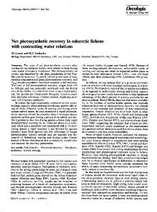
Fig. 8 Cost decrement of optimization trials with arbitrary initial candidates
Algorithm 1: Compaction optimization algorithm
(a)
(c)
(b)
Fig. 9 Optimization efficiency of various circuits
Fig. 7 (a) Inital placement with MHS partition (b) Placement constraints (c) Placement after compaction optimization date, its impact to the circuit performance is evaluated and compared to the lowest cost candidate currently found (line 7). The candidate is accepted if the cost difference
e –∆ C ⁄ T where
P
satisfies
P,
(6)
0, 1 ]. If 1, acceptance is thus guaranteed. A
is drawn from the uniform distributed interval [
the new cost is lower, linear
>
∆C
e –∆ C ⁄ T
>
cooling schedule is used in our implementation, which gradT
ually lowers the virtual temperature
as the search progresses
(line 14). This reduces the likelihood of (6) to be satisfied for steps that increases cost
∆
C>0.
Upon reaching the pre-determined
number of iterations, the algorithm returns with a list of the lowest cost compaction configurations.
4.2 Cost Functions
Circuit simulators facilitate calculation (e.g. SENS in SPICE) of both the DC operating-point and AC small-signal sensitivities ∂ f ⁄ ∂ x of an output variable f with respect to any circuit parasitic values x . The cost function with respect to f is 1 -. C ( x ) = ----------------------------------(7) .
f
f
+ ∂f ⁄ ∂x
t
⋅ ∆x
∆ x results from block displacements are computed according to (1) and (2) for the substrate coupling network and interconnect parasitics respectively.
4.3 Compaction Optimization Examples
multaneously optimized. The average execution time is 6.006s for 2000 iterations on a UNIX computation server. In order to examine the efficiency of the algorithm, 3 analog circuits of various sizes are optimized. Each design is propagated with 10 sets of randomly generated performance sensitivities, in order to represent distinctive circuits of the same size. Each set is optimized 50 times for 200 iterations. Fig. 9 plots the average execution time versus the circuit block and parasitic device counts. Expectedly, the execution time depends linearly on the total number of parasitic devices, instead of block count nor circuit types, as most time is spent by performance cost computation. V. CONCLUSIONS A compaction algorithm that optimizes the placement of guard bands and circuit blocks for analog circuits using simulated annealing technique was proposed to minimize layout parasitic effects for analog circuits in the DSM mixed-signal environment. Through the use of sensitivity-based cost functions, the impact of interconnect and substrate parasitics are quantified. Performance improvement is demonstrated while the customized layout topology, symmetry and matching constraints are preserved. VI. REFERENCES [1] Glelen, G., et. al., When wi ll the anal og design flow catch up wi th di gital
methodol ogy ?
IEEE Design Automation Conference,
2001.
Proceedi ngs pp: 419 - 419 2001. [2] Cong, J., et al ., “Dynamic
weighti ng
Monte
Carlo
fl oorpl an desi gns in mixed si gnal appl ication”,
for
constrai ned
Proceedings of the
ASP Design Automation Conference , pp:277 - 282, Jan. 2000.
[3] Zhang, L., Raut, R., Jiang, Y., Kl ei ne, U., “Placement A lgori thm in
Desi gns”, IEEE Transactions on Computer-Aided Design of Integrated Circuits and Systems, Vol25, Issue 10, pp:1889 A nal og-Lay out
- 1903 , Oct. 2006. [4] Zhang. L., Kl ei ne, U.,
“A
genetic approach to anal og module place-
IEEE International Symposium on Circuits and Systems, Vol. 1, pp:345- 348, 2002. nd [5] Hastings, A ., Art of Analog Layout, 2 Ed., Prentice Hall, Boston, ment with simul ated anneal ing”,
An analog operational amplifier circuit with 15 device blocks and 5 guard bands is shown in Fig. 7(a). It has 7 self-symmetry and 4 mirror symmetry constraints. 10 optimization trials each with 2000 iterations are performed. Parasitic cost reductions are shown in Fig. 8. An interesting observation is that the ultimate optimization results have some dependence on the starting points. Hence, it is advantageous to break down long iterations into several trials that restart at a new state. The placement of the best compaction candidate is shown in Fig. 7(c). Guard bands placements are si-
2005.
Algorithms for VLSI Physical Design Automation (3rd Ed.), Kl uwer A cademic Publishers, Boston, 1999.
[6] Sherwani, N. A .,
[7] Samavedam, A ., et. al ., “A Scal abl e Substrate Noise Coupl ing Model
IEEE Journal of Solid-State Circuits, vol. 35, no. 6, pp.895- 904, Jun. 2000. for Design of Mixed- Signal I C’s”,
[8] Hardwick, J.C., “Impl ementati on and eval uati on of an efficient paral-
2937
, Proc. of 9th ACM symposium on Parallel algorithms and architectures, pp:: 239 - 248, 1997. lel Delaunay triangulati on algori thm”