applied sciences Article
A Polarization-Dependent Frequency-Selective Metamaterial Absorber with Multiple Absorption Peaks Guangsheng Deng, Tianyu Xia, Yong Fang, Jun Yang and Zhiping Yin * Academy of Photoelectric Technology, Hefei University of Technology, Key Lab of Special Display Technology, Ministry of Education, No. 193, Tunxi Road, Hefei 230009, China;
[email protected] (G.D.);
[email protected] (T.X.);
[email protected] (Y.F.);
[email protected] (J.Y.) * Correspondence:
[email protected]; Tel.: +86-551-6290-2791 Academic Editor: Kenneth Chau Received: 19 April 2017; Accepted: 31 May 2017; Published: 4 June 2017
Abstract: A polarization-dependent, frequency-selective metamaterial (MM) absorber based on a single-layer patterned resonant structure intended for F frequency band is proposed. The design, fabrication, and measurement for the proposed absorber are presented. The absorber’s absorption properties at resonant frequencies have unique characteristics of a single-band, dual-band, or triple-band absorption for different polarization of the incident wave. The calculated surface current distributions and power loss distribution provide further understanding of physical mechanism of resonance absorption. Moreover, a high absorption for a wide range of TE-polarized oblique incidence was achieved. Hence, the MM structure realized on a highly flexible polyimide film, makingthe absorber suitable for conformal geometry applications. The proposed absorber has great potential in the development of polarization detectors and polarizers. Keywords: absorber; metamaterial; multi-band absorption; polarization-dependent
1. Introduction Electromagnetic metamaterials, which represent a class of artificial structures whose electric and magnetic response can be controlled freely, have attracted a significant amount of attention [1–3]. Due to their unique benefits, metamaterials have provided many important effects, such as invisible cloaking [4], negative refractive index [5], and super-lens [6]. Since the metamaterial absorber (MA) was presented in 2008 by Landy et al. [7], metamaterial has attracted many researchers because of its advantages, such as size minimization and suitable thickness, for applications using electromagnetic wave absorbers [8–10]. In recent years, various structures, such as split rings [11], closed rings [12], and fishnet structures [13], have been proposed for MAs. A certain progress has been made in broadband MAs developing [14,15]. Meanwhile, some studies on tunable absorbers [16,17] and multiband absorbers [18–20] have been performed. Currently, research is focused on absorbers intended for application in polarization imaging and polarization detecting. Therefore, the polarization-dependent frequency-selective absorbers are highly demanded. For most single patterned resonant structures, the number of absorption peaks was fixed or the absorbers were polarization-independent [21,22]. Hokmabadi et al. proposed a stereometamaterial perfect absorber, wherein absorption frequency is related to polarization angles [23]. Hu et al. presented a polarization-dependent MA with different resonant frequencies in two orthogonal directions [24]. However, these structures have only one polarization-dependent absorption peak, which limits their application in spectroscopic imaging and detecting, wherein multiple absorption peaks are required [25,26].
Appl. Sci. 2017, 7, 580; doi:10.3390/app7060580
www.mdpi.com/journal/applsci
Appl. Sci. 2017, 7, 580
2 of 9
In this paper, the focus is on the F frequency band (F-band), and a simple polarization- dependent Appl. Sci. 2017, 7, 580 2 of 9 frequency-selective metamaterial absorber is proposed. The proposed structure has three separate absorption with the highfocus absorption forF TE-polarized and(F‐band), TM-polarized normalpolarization‐ incident waves. In peaks this paper, is on the frequency band and a simple Furthermore, the absorption peaks can be dynamically controlled by adjusting of a polarization angle dependent frequency‐selective metamaterial absorber is proposed. The proposed structure has three of theseparate absorption peaks with high absorption for TE‐polarized and TM‐polarized normal incident incident wave. Compared to the previously reported MAs, the MA proposed in this paper waves. Furthermore, Firstly, the absorption peaks can be resonance dynamically controlled by multiple adjusting absorption of a has several advantages. compared to complex structures with polarization angle of the incident wave. Compared to the previously reported MAs, the MA proposed peaks, such as all-in-one packed super-unit cell [27,28] and stacked layers [29], the proposed absorber in this paper has several advantages. Firstly, compared to complex resonance structures with has only one patterned resonant structure, which meets current demands on miniaturization and multiple absorption peaks, such as all‐in‐one packed super‐unit cell [27,28] and stacked layers [29], simplification. Secondly, the multiple absorption peaks can be dynamically tuned by changing of the proposed absorber has only one patterned resonant structure, which meets current demands on polarization angles of the incident wave. Lastly, the proposed MA structure is realized on a highly miniaturization and simplification. Secondly, the multiple absorption peaks can be dynamically flexible polyimide film without a rigid substrate, so the absorber can be easily used in the non-planar tuned by changing of polarization angles of the incident wave. Lastly, the proposed MA structure is and conformal-geometry applications. realized on a highly flexible polyimide film without a rigid substrate, so the absorber can be easily used in the non‐planar and conformal‐geometry applications.
2. Structure and Design
2. Structure and Design
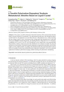
The proposed MA structure and the unit cell structure of the copper pattern are presented in Figure 1.The proposed MA structure and the unit cell structure of the copper pattern are presented in Unlike previously reported results, where multiple different-sized metal patterns were Figure 1. Unlike previously reported results, where multiple different‐sized metal patterns were used used to obtain multi-band absorption, here, the simple etching of a C-shaped slot into a circular to provides obtain multi‐band absorption, here, the of a C‐shaped a circular patch, a triple-band absorption. Thesimple etching geometrical dimensions of slot into the copper patternpatch, shown in provides a triple‐band absorption. The geometrical dimensions of the copper pattern shown in Figure Figure 1b are a = 820 µm, d = 60 µm, r1 = 112.5 µm, r2 = 161 µm, and r3 = 367.5 µm. The copper pattern 1b are a = 820 μm, d = 60 μm, r1 = 112.5 μm, r2 = 161 μm, and r3 = 367.5 μm. The copper pattern with a with thickness of 0.5 μm and an electric conductivity of (5.8×10 a thickness of 0.5 µm and an electric conductivity of (5.8 ×10⁷ ) S/m was printed on the top layer 7) S/m was printed on the top layer of a of a thick dielectric substrate with a thickness of 50 µm that was made of polyimide film with a relative thick dielectric substrate with a thickness of 50 μm that was made of polyimide film with a relative permittivity of 3.6 and a dielectric loss tangent of 0.02. Moreover, a thick copper plate that acts as a permittivity of 3.6 and a dielectric loss tangent of 0.02. Moreover, a thick copper plate that acts as a ground plane was printed on the bottom of the dielectric substrate. ground plane was printed on the bottom of the dielectric substrate.
Figure 1. (a) The proposed metamaterial absorber (MA) unit cell structure; (b) layout of the unit cell Figure 1. (a) The proposed metamaterial absorber (MA) unit cell structure; (b) layout of the unit cell 2 = 161, and r3 = 367.5. structure and its optimal values given in micrometers: a = 820, d = 60, r structure and its optimal values given in micrometers: a = 820, d = 60, 1r = 112.5, r 1 = 112.5, r2 = 161, and r3 = 367.5.
The absorptivity can be calculated by
The absorptivity can be calculated by
A = 1 − |S11|2 − |S21|2 2
(1) 2
A = 1 − |S11 | − |S21 | (1) where A, S11, and S21 are the absorptivity, the reflection coefficient, and the transmission coefficient, respectively. In this case, the transmission coefficient S21 is zero because the thickness of the metal where A, S11 , and S21 are the absorptivity, the reflection coefficient, and the transmission coefficient, ground plane is much larger than its skin depth, so the absorptivity is determined by A = 1 − |S 11|2. respectively. In this case, the transmission coefficient S21 is zero because the thickness of the metal 3. SimulatedResultsandDiscussion ground plane is much larger than its skin depth, so the absorptivity is determined by A = 1 − |S11 |2 . The simulations were conducted in CST Microwave Studio 2014 (Darmstadt, Germany), using
3. Simulated Results and Discussion the finite‐element frequency‐domain method, and the unit cell boundary conditions were utilized in
both x and y directions. Meanwhile, the Floquet port condition was employed in the z‐direction. Since The simulations were conducted in CST Microwave Studio 2014 (Darmstadt, Germany), using the proposed absorber has similar absorption characteristics for TE‐polarized and TM‐polarized the finite-element frequency-domain method, and the unit cell boundary conditions were utilized normal incident waves, only the electromagnetic responses for the TE‐polarized incident wave, in both x and y directions. Meanwhile, the Floquet port condition was employed in the z-direction. whose electric field is parallel to the x‐axis, were calculated for the normal incidence angle. Three Since the proposed absorber has similar absorption characteristics for TE-polarized and TM-polarized
Appl. Sci. 2017, 7, 580
3 of 9
Appl. Sci. 2017, 7, 580 3 of 9 normal incident waves, only the electromagnetic responses for the TE-polarized incident wave, whose electric field is parallel to the x-axis, were calculated for the normal incidence angle. Three distinct distinct absorption peaks, which are at 92.4 GHz, 102.0 GHz, and 130.1 GHz with absorptivities of absorption peaks, which are at 92.4 GHz, 102.0 GHz, and 130.1 GHz with absorptivities of 88.1%, 88.1%, 98.2%, and 94.6%, respectively, are presented in Figure 2. In addition, three resonance peaks 98.2%, and 94.6%, respectively, are presented in Figure 2. In addition, three resonance peaks were were labeled as mode f 1, mode f2, and mode f3 starting from low to high frequencies. From Figure 2, labeled as mode f 1 , mode f 2 , and mode f 3 starting from low to high frequencies. From Figure 2, the the separation of the first two adjacent resonant peaks of the MA is not high enough, which may separation of the first two adjacent resonant peaks of the MA is not high enough, which may hinder its hinder its applications in the multiband detection. This can be improved by reconstructing the applications in the multiband detection. This can be improved by reconstructing the geometries of the geometries of the proposed structure. proposed structure.
Figure 2. 2. Absorption Absorption spectra spectra of of the the proposed proposed metamaterial metamaterial absorber absorber for for the the TE-polarized TE‐polarized normal normal Figure incident wave. incident wave.
In order to show the intrinsic mechanism of the proposed metamaterial absorber, the surface In order to show the intrinsic mechanism of the proposed metamaterial absorber, the surface currents distributed on on the the metal metal pattern pattern and and the the metal metal ground ground plane plane that that correspond correspond to to three three currents distributed absorption peaks were calculated and the obtained results are presented in Figure 3. absorption peaks were calculated and the obtained results are presented in Figure 3. As shown in Figure 3a, for mode f As shown in Figure 3a, for mode f 11, the surface currents on the metal pattern diverge from inner , the surface currents on the metal pattern diverge from inner circular patch to two arms of the closed ring, and then converge to the lower left corner of the ring, circular patch to two arms of the closed ring, and then converge to the lower left corner of the ring, which means that mode f which means that mode f 11 represents a typical dipole resonance. Meanwhile, the surface currents on represents a typical dipole resonance. Meanwhile, the surface currents on the metal ground plane, shown in Figure 3b, are reversed, and circulating current loops are formed the metal ground plane, shown in Figure 3b, are reversed, and circulating current loops are formed because the current on two metal layers are anti‐parallel, so the magnetic response is excited. because the current on two metal layers are anti-parallel, so the magnetic response is excited. Similarly, for mode f Similarly, for mode f 2 ,2, the electric response is excited by surface currents on the metal pattern the electric response is excited by surface currents on the metal pattern that that two of arms of the ring, closed ring, forming dipole resonance (Figure 3c). However, flow flow alongalong two arms the closed forming a dipolea resonance (Figure 3c). However, compare compare with mode f 1, the surface currents on the closed ring in mode f2 diverge from the lower right with mode f 1 , the surface currents on the closed ring in mode f 2 diverge from the lower right corner corner and converge to the left upper left According corner. According results presented 3d, the and converge to the upper corner. to resultsto presented in Figure in 3d,Figure the magnetic magnetic response of mode f 2 is also excited by circulating currents between two metal layers. In the response of mode f 2 is also excited by circulating currents between two metal layers. In the case of case of mode f 3, the surface currents are mainly concentrated on the connecting bar between a circular mode f 3 , the surface currents are mainly concentrated on the connecting bar between a circular patch patch and a closed ring (Figure 3e), and mode f 3 represents a dipole resonance that mainly depends and a closed ring (Figure 3e), and mode f 3 represents a dipole resonance that mainly depends on the on the connecting bar dimensions. connecting bar dimensions. In order to demonstrate the absorption mechanism, the power loss density in the dielectric layer In order to demonstrate the absorption mechanism, the power loss density in the dielectric layer and the ohmic losses at resonator surface for mode f and the ohmic losses at resonator surface for mode f 11 − f − f33 were determined, and the obtained results were determined, and the obtained results are illustrated in Figures 4 and 5, respectively. Dielectric of the are mainly are illustrated in Figures 4 and 5, respectively. Dielectric losses of losses the absorber areabsorber mainly concentrated concentrated in areas with a strong electric field, while the ohmic losses at resonator surface are in areas with a strong electric field, while the ohmic losses at resonator surface are determined by determined by surface currents. In addition, it has been observed that the power losses in are the surface currents. In addition, it has been observed that the power losses in the dielectric layer dielectric layer are more than dissipated on the resonator surface, and the polyimide film has a very more than dissipated on the resonator surface, and the polyimide film has a very important role in the important role in the absorption of the incident waves. absorption of the incident waves.
Appl. Sci. 2017, 7, 580 Appl. Sci. 2017, 7, 580 Appl. Sci. 2017, 7, 580
4 of 9 4 of 9 4 of 9
Figure 3. Simulated surface current distribution on (a) a metal pattern at 92.4 GHz; (b) a metal ground Figure 3. Simulated surface current distribution on (a) a metal pattern at 92.4 GHz; (b) a metal ground Figure 3. Simulated surface current distribution on (a) a metal pattern at 92.4 GHz; (b) a metal ground plane at 92.4GHz; (c) a metal pattern at 102.0 GHz; (d) a metal ground plane at 102.0 GHz; (e) a metal plane at 92.4GHz; (c) a metal pattern at 102.0 GHz; (d) a metal ground plane at 102.0 GHz; (e) a metal plane at 92.4GHz; (c) a metal pattern at 102.0 GHz; (d) a metal ground plane at 102.0 GHz; (e) a metal pattern at130.1 GHz and (f) a metal ground plane at 130.1 GHz. pattern at130.1 GHz and (f) a metal ground plane at 130.1 GHz. pattern at130.1 GHz and (f) a metal ground plane at 130.1 GHz.
Figure 4. Distribution of dielectric power losses on polyimide film at (a) 92.4 GHz; (b) 102.0 GHz, and Figure 4. Distribution of dielectric power losses on polyimide film at (a) 92.4 GHz; (b) 102.0 GHz, and Figure 4. Distribution of dielectric power losses on polyimide film at (a) 92.4 GHz; (b) 102.0 GHz, and (c) 130.1 GHz. (c) 130.1 GHz. (c) 130.1 GHz.
Appl. Sci. 2017, 7, 580 Appl. Sci. 2017, 7, 580
5 of 9
Figure 5. Distribution of ohmic losses on resonator surface at (a) 92.4 GHz; (b) 102.0 GHz and (c) 130.1 GHz. 5 of 9
4. MA Absorption Dependence on the Wave Incident Angle and Polarization The absorption characteristics of the proposed structure for oblique incident wave with TE polarization were simulated, and the obtained results are shown in Figure 6a. During the calculation, E‐field was in the x‐direction, and H‐field and wave propagation directions varied simultaneously for angle θ.As shown in Figure 6a, when the oblique incident angle increases from 0 to 60°, the absorption peaks at the three resonance frequencies are about 90% or greater, which is caused by a resonator structure, wherein for TE polarization a strong electric resonance can be excited with a relatively small field strength. For the TM‐polarized wave, whose H‐field is in the x‐direction, the absorption characteristics for the oblique incident wave were also simulated, and the obtained results are shown in Figure 6b. However, as can be seen in Figure 6b, when the incident angle increases, the absorption characteristic Figure 5. Distribution of ohmic losses on resonator surface at (a) 92.4 GHz; (b) 102.0 GHz and Figure 5. Distribution of ohmic losses on resonator surface at (a) 92.4 GHz; (b) 102.0 GHz and (c) 130.1 GHz. for TM‐polarized oblique incidence deteriorates rapidly at all resonance modes. (c) 130.1 GHz. Nonetheless, we were focused on absorption characteristics for different polarization angles for 4. MA Absorption Dependence on the Wave Incident Angle and Polarization the normal incident wave. For TE and TM polarization, E‐field changes for angle φ with respect to 4. MA Absorption Dependence on the Wave Incident Angle and Polarization The absorption characteristics the proposed responses structure for for TE oblique incident wave with TE the x‐and y‐direction, respectively. of The simulated and TM waves for different The absorption characteristics of the proposed structure for oblique incident wave with TE polarization were simulated, and the obtained results are shown in Figure 6a. During the calculation, polarization angles are presented in Figure 7a and Figure 7b, respectively. As shown in Figure 7a, for polarization were simulated, and the obtained results are shown in Figure 6a. During the calculation, E‐field was in the x‐direction, and H‐field and wave propagation directions varied simultaneously resonant modes f1 and f3, the absorption is high when φ is in the range 0–45°. However, the resonance E-field was in the x-direction, and6a, H-field and wave propagation varied from simultaneously for for angle θ.As shown in Figure when the oblique incident directions angle increases 0 to 60°, the of mode f 2 decreases gradually when φ changes from 0 to 45°. According to results presented in Figure ◦ angle θ.As shown in Figure 6a, when the oblique incident angle increases from 0 to 60 , the absorption absorption peaks at the three resonance frequencies are about 90% or greater, which is caused by a 7a, it can be concluded that the resonance of mode f2 vanishes at φ = 45° because the surface current peaks at the three resonance frequencies are about 90% orelectric greater,resonance which is caused by a resonator resonator structure, wherein for TE polarization a strong can be excited with a on the resonator surface in mode f 2 (Figure 3c) mainly flows perpendicularly to the direction of the structure, wherein for TE polarization a strong electric resonance can be excited with a relatively small relatively small field strength. electric field vector. Therefore, the electric response cannot be excited. fieldFor the TM‐polarized wave, whose H‐field is in the x‐direction, the absorption characteristics for strength. the oblique incident wave were also simulated, and the obtained results are shown in Figure 6b. However, as can be seen in Figure 6b, when the incident angle increases, the absorption characteristic for TM‐polarized oblique incidence deteriorates rapidly at all resonance modes. Nonetheless, we were focused on absorption characteristics for different polarization angles for the normal incident wave. For TE and TM polarization, E‐field changes for angle φ with respect to the x‐and y‐direction, respectively. The simulated responses for TE and TM waves for different polarization angles are presented in Figure 7a and Figure 7b, respectively. As shown in Figure 7a, for resonant modes f1 and f3, the absorption is high when φ is in the range 0–45°. However, the resonance of mode f2 decreases gradually when φ changes from 0 to 45°. According to results presented in Figure 7a, it can be concluded that the resonance of mode f2 vanishes at φ = 45° because the surface current on the resonator surface in mode f2 (Figure 3c) mainly flows perpendicularly to the direction of the electric field vector. Therefore, the electric response cannot be excited. Figure 6. Simulated responses of the structure for different incident angles θ for (a) the TE-polarized Figure 6. Simulated responses of the structure for different incident angles θ for (a) the TE‐polarized wave and (b) the TM-polarized wave. wave and (b) the TM‐polarized wave.
For the TM-polarized wave, whose H-field is in the x-direction, the absorption characteristics for the oblique incident wave were also simulated, and the obtained results are shown in Figure 6b. However, as can be seen in Figure 6b, when the incident angle increases, the absorption characteristic for TM-polarized oblique incidence deteriorates rapidly at all resonance modes. Nonetheless, we were focused on absorption characteristics for different polarization angles for the normal incident wave. For TE and TM polarization, E-field changes for angle ϕ with respect to the x-and y-direction, respectively. The simulated responses for TE and TM waves for different polarization angles are presented in Figure 7a,b, respectively. As shown in Figure 7a, for resonant modes f 1 and f 3 , the absorption is high when ϕ is in the range 0–45◦ . However, the resonance of mode f 2 decreases gradually when ϕ changes from 0 to 45◦ . According to results presented in Figure 7a, it Figure 6. Simulated responses of the structure for different incident angles θ for (a) the TE‐polarized can be concluded that the resonance of mode f 2 vanishes at ϕ = 45◦ because the surface current on the wave and (b) the TM‐polarized wave. resonator surface in mode f 2 (Figure 3c) mainly flows perpendicularly to the direction of the electric field vector. Therefore, the electric response cannot be excited.
Appl. Sci. 2017, 7, 580 Appl. Sci. 2017, 7, 580 Appl. Sci. 2017, 7, 580
66 of 9 of 9 6 of 9
Figure 7. Simulated absorption characteristic of the proposed structure for different polarization Figure 7. characteristic of the proposed structure for different polarization angles Figure 7. Simulated Simulated absorption absorption characteristic of the proposed structure for different polarization angles φ for (a) the TE‐polarized wave and (b) the TM‐polarized wave. ϕ for (a) the TE-polarized wave and (b) the TM-polarized wave. angles φ for (a) the TE‐polarized wave and (b) the TM‐polarized wave.
Similarly, when TM polarization angle is changed, the absorption peaks for mode f2 are above Similarly, when TM polarization angle is changed, the absorption peaks for mode f Similarly, TM polarization angle is fchanged, the absorption peaks for mode f 22 are above are above 80%, while the when absorptivities of mode f1 and 3 decrease gradually when φ changes from 0 to 45°. 80%, while the absorptivities of mode f 1 and f 3 decrease gradually when φ changes from 80%, while the absorptivities of mode f 1 and f 3 decrease gradually when ϕ changes from0 0 to to 45°. 45◦ . Therefore, the proposed structure provides both single‐band and multi‐band absorption for different Therefore, the proposed structure provides both single‐band and multi‐band absorption for different Therefore, the proposed structure provides both single-band and multi-band absorption for different polarization angles. polarization angles. polarization angles. 5. Experimental Results 5. Experimental Results 5. Experimental Results The MA was fabricated using standard photolithography. Firstly, the copper with a thickness of The MA was fabricated using standard photolithography. Firstly, the copper with a thickness of The MA was fabricated using standard photolithography. Firstly, the copper with a thickness 0.5 μm was deposited on the bottom surface of the polyimide film. Then, the photolithography was 0.5 μm was deposited on the bottom surface of the polyimide film. Then, the photolithography was of 0.5 µm was deposited on the bottom surface of the polyimide film. Then, the photolithography used to define the metallic patterned resonator at the top film surface. Lastly, the copper was used to define the the metallic patterned resonator at at the top was used to define metallic patterned resonator the topfilm filmsurface. surface.Lastly, Lastly,the the copper copper was was evaporated, and a metal lift‐off process was used to complete the pattern transfer. The fabricated evaporated, was used used to to complete complete the the pattern pattern transfer. transfer. The fabricated evaporated, and and a a metal metal lift‐off lift-off process process was The fabricated sample composed by 18×18 unit‐cells with a dimension of 1.5 cm×1.5 cm is displayed in Figure 8. sample composed by 18×18 unit‐cells with a dimension of 1.5 cm×1.5 cm is displayed in Figure 8. sample composed by 18×18 unit-cells with a dimension of 1.5 cm×1.5 cm is displayed in Figure 8.
Figure 8. Fabricated metamaterial absorber: (a) real size; (b) enlarged portion. Figure 8. Fabricated metamaterial absorber: (a) real size; (b) enlarged portion. Figure 8. Fabricated metamaterial absorber: (a) real size; (b) enlarged portion.
The free space measurement method was adopted in the experiment. A pair of horn antennas The free space measurement method was adopted in the experiment. A pair of horn antennas The free space measurement method was adopted in the experiment. A pair of horn antennas were the Agilent N5224A vector network analyzer (Agilent Technologies Inc, Santa were connected connected toto the Agilent N5224A vector network analyzer (Agilent Technologies Inc, Clara, Santa were connected to the Agilent N5224A vector network analyzer (Agilent Technologies Inc, Santa CA, USA) via VNA extenders VDI VNAX600 (Virginia Diodes Inc, Charlottesville, VA, USA) that were Clara, CA, USA) via VNA extenders VDI VNAX600 (Virginia Diodes Inc, Charlottesville, VA, USA) Clara, CA, USA) via VNA extenders VDI VNAX600 (Virginia Diodes Inc, Charlottesville, VA, USA) used for frequency range 90–140 GHz. In this case, one antenna acted as a transmitting antenna and that were used for frequency range 90–140 GHz. In this case, one antenna acted as a transmitting that were used for frequency range 90–140 GHz. In this case, one antenna acted as a transmitting other as a receiving antenna. In order to avoid the reflections from the environment, the calibration was antenna and other as a receiving antenna. In order to avoid the reflections from the environment, the antenna and other as a receiving antenna. In order to avoid the reflections from the environment, the performed as follows. The reflections from an identical copper plate, which acts as an ideal reflector, calibration was performed as follows. The reflections from an identical copper plate, which acts as an calibration was performed as follows. The reflections from an identical copper plate, which acts as an were firstly measured. Then, the actual reflections from the sample were calculated by comparison ideal reflector, were firstly measured. Then, the actual reflections from the sample were calculated by ideal reflector, were firstly measured. Then, the actual reflections from the sample were calculated by of the reflection from the structure and the reflection from the copper plate. It should be noted that, comparison of the reflection from the structure and the reflection from the copper plate. It should be comparison of the reflection from the structure and the reflection from the copper plate. It should be for the given sample dimensions, a minimum far-field distance of 40 cm must be met. Moreover, noted that, for the given sample dimensions, a minimum far‐field distance of 40 cm must be met. noted that, for the given sample dimensions, a minimum far‐field distance of 40 cm must be met.
Appl. Sci. 2017, 7, 580 Appl. Sci. 2017, 7, 580
77 of 9 of 9
Moreover, the measurement of responses for different incident angles has not been carried out due the measurement of responses for different incident angles has not been carried out due to the large to the large scattering of this finite sample at wide incident angles [30]. scattering of this finite sample at wide incident angles [30]. The measured MA absorption for various polarization angles (φ) for both TE‐polarized and TM‐ The measured MA absorption for various polarization angles (ϕ) for both TE-polarized and polarized normal incident waves is presented in Figure 9. For TE‐polarization, a dual‐band TM-polarized normal incident waves is presented in Figure 9. For TE-polarization, a dual-band absorption is achieved for a polarization angle of 45°. However, only one absorption peak with absorption is achieved for a polarization angle of 45◦ . However, only one absorption peak with absorptivity of above 70% is achieved for polarization angle ◦of 45° in the case of TM‐polarized absorptivity of above 70% is achieved for polarization angle of 45 in the case of TM-polarized incident incident wave, which is in agreement with the simulated results. wave, which is in agreement with the simulated results.
Figure Measured MA for different polarization angles for for (a) the TE-polarized wavewave and Figure 9. 9. Measured MA absorption absorption for different polarization angles (a) the TE‐polarized (b) the TM-polarized wave. and (b) the TM‐polarized wave.
6. Conclusions 6. Conclusions A simple design of a polarization-dependent frequency-selective metamaterial absorber based A simple design of a polarization‐dependent frequency‐selective metamaterial absorber based on a circular patch with a C-shaped slot is presented. In contrast to previous studies on on a circular patch with a C‐shaped slot is presented. In contrast to previous studies on compression compression of multiin resonators, in thedesign, proposed design, a multi-band is using obtained using of multi resonators, the proposed a multi‐band absorption absorption is obtained a simple aresonant structure. Furthermore, changing the polarization angle of the incident wave, a triple‐band, simple resonant structure. Furthermore, changing the polarization angle of the incident wave, a triple-band, a dual-band, and a single-band absorptions can be achieved, which is required in the a dual‐band, and a single‐band absorptions can be achieved, which is required in the polarization‐ polarization-dependent detection. In demonstrate order to demonstrate the absorption mechanism, the electric dependent detection. In order to the absorption mechanism, the electric field field distribution, the surface current distribution, and the power-loss distributions were obtained. distribution, the surface current distribution, and the power‐loss distributions were obtained. The The proposed design was verified both by simulations and experiments, which were performed using proposed design was verified both by simulations and experiments, which were performed using the the free space measurement method. A good agreement between simulated and measured results was free space measurement method. A good agreement between simulated and measured results was achieved, which proves a high absorption performance of the proposed MA. achieved, which proves a high absorption performance of the proposed MA. Acknowledgments: This work was supported by the National Natural Science Foundation of China (No. 51607050) Acknowledgments: This work was supported by the National Natural Science Foundation of China (No. and the National Defense Pre-Research Foundation of China (Grant No. 6140239010106). 51607050) and the National Defense Pre‐Research Foundation of China (Grant No. 6140239010106). Author Contributions: Guangsheng Deng and Zhiping Yin conceived and wrote the paper; Tianyu Xia and Author Contributions: and Zhiping Yin conceived and wrote paper; the Tianyu Yong Fang performed theGuangsheng experiments;Deng Jun Yang guided the experimental design andthe analyzed data.Xia and Yong Fang performed the experiments; Jun Yang guided the experimental design and analyzed the data. Conflicts of Interest: The authors declare no conflict of interest.
Conflicts of Interest: The authors declare no conflict of interest.
References References
1. 1. 2.
3. 4. 4.
5.
Smith, D.; Pendry, J.; Wiltshire, M. Metamaterials and negative refractive index. Science 2004, 305, 788–792. Smith, D.; Pendry, J.; Wiltshire, M. Metamaterials and negative refractive index. Science 2004, 305, 788–792. [CrossRef] [PubMed] Chen, H.T.; Padilla, W.J.; Zide, J.M.; Gossard, A.C.; Taylor, A.J.; Averitt, R.D. Active terahertz metamaterial Chen, H.T.; Padilla, W.J.; Zide, J.M.; Gossard, A.C.; Taylor, A.J.; Averitt, R.D. Active terahertz metamaterial devices. Nature 2006, 444, 597–600. [CrossRef] [PubMed] devices. Nature 2006, 444, 597–600. Poddubny, A.; Iorsh, I.; Belov, P.; Kivshar, Y. Hyperbolic Metamaterials. Nat. Photonics 2013, 7, 948–957. Poddubny, A.; Iorsh, I.; Belov, P.; Kivshar, Y. Hyperbolic Metamaterials, Nat. Photonics 2013, 7, 948–957. [CrossRef] Chen, H.S.; Wu, B.I.; Zhang, B.; Kong, J.A. Electromagnetic wave interactions with a metamaterial cloak. Chen, H.S.; Wu, B.I.; Zhang, B.; Kong, J.A. Electromagnetic wave interactions with a metamaterial cloak. Phys. Rev. Lett. 2007, 99, 063903. Phys. Rev. Lett. 2007, 99, 063903. [CrossRef] [PubMed] Valentine, J.; Zhang, S.; Zentgraf, T.; Ulin‐Avila, E.; Genov, D.A.; Bartal, G.; Zhang, X. Three‐dimensional optical metamaterial with a negative refractive index. Nature 2008, 455, 376–379.
Appl. Sci. 2017, 7, 580
5. 6. 7. 8. 9.
10. 11. 12. 13. 14. 15. 16. 17. 18. 19. 20.
21. 22. 23. 24.
25. 26.
27. 28.
8 of 9
Valentine, J.; Zhang, S.; Zentgraf, T.; Ulin-Avila, E.; Genov, D.A.; Bartal, G.; Zhang, X. Three-dimensional optical metamaterial with a negative refractive index. Nature 2008, 455, 376–379. [CrossRef] [PubMed] Kaina, N.; Lemoult, F.; Fink, M.; Lerosey, G. Negative refractive index and acoustic superlens from multiple scattering in single negative metamaterials. Nature 2015, 525, 77–81. [CrossRef] [PubMed] Landy, N.; Sajuyigbe, S.; Mock, J.; Smith, D.; Padilla, W. Perfect metamaterial absorber. Phys. Rev. Lett. 2008, 100, 207402. [CrossRef] [PubMed] Yin, S.; Zhu, J.F.; Xu, W.D.; Jiang, W.; Yuan, J.; Yin, G.; Xie, L.J.; Ying, Y.B.; Ma, Y.G. High-performance terahertz wave absorbers made of silicon-based metamaterials. Appl. Phys. Lett. 2015, 107, 073903. [CrossRef] Huang, L.; Chowdhury, D.R.; Ramani, S.; Reiten, M.T.; Luo, S.N.; Taylor, A.J.; Chen, H.T. Experimental demonstration of terahertz metamaterial absorbers with a broad and flat high absorption band. Opt. Lett. 2012, 37, 154–156. [CrossRef] [PubMed] Shi, C.; Zang, X.F.; Wang, Y.Q.; Chen, L.; Cai, B.; Zhu, Y.M. A polarization-independent broadband terahertz absorber. Appl. Phy. Lett. 2014, 105, 031104. [CrossRef] Zhu, W.R.; Huang, Y.J.; Rukhlenko, I.D.; Wen, G.J.; Premaratne, M. Configurable metamaterial absorber with pseudo wideband spectrum. Opt. Express 2012, 20, 6612–6621. [CrossRef] [PubMed] Wang, B.X.; Zhai, X.; Wang, G.Z.; Huang, W.Q.; Wang, L.L. Design of a Four-Band and Polarization-Insensitive Terahertz Metamaterial Absorber. IEEE Photonics J. 2015, 7, 4600108. [CrossRef] Faraji, M.; Morawej-Farshi, M.K.; Yousefi, L. Tunable THz perfect absorber using graphene-based metamaterials. Opt. Commun. 2015, 355, 352–355. [CrossRef] Zhu, J.F.; Ma, Z.F.; Sun, W.J.; Ding, F.; He, Q.; Zhou, L.; Ma, Y.G. Ultra-broadband terahertz metamaterial absorber. Appl. Phys. Lett. 2014, 105, 021102. [CrossRef] He, X.J.; Yan, S.T.; Ma, Q.X.; Zhang, Q.F.; Jia, P.; Wu, F.M.; Jiang, J.X. Broadband and polarization-insensitive terahertz absorber based on multilayer metamaterial. Opt. Commun. 2015, 340, 44–49. [CrossRef] Shrekenhamer, D.; Chen, W.C.; Padilla, W.J. Liquid Crystal Tunable Metamaterial Absorber. Phys. Rev. Lett. 2013, 110, 177403. [CrossRef] [PubMed] Zhang, Y.; Feng, Y.; Zhu, B. Graphene based tunable metamaterial absorber and polarization modulation in terahertz frequency. Opt. Express 2014, 22, 22743–22752. [CrossRef] [PubMed] Yahiaoui, R.; Guillet, J.P.; de Miollis, F.; Mounaix, P. Ultra-flexible multiband terahertz metamaterial absorber for conformal geometry applications. Opt. Lett. 2013, 38, 4988–4990. [CrossRef] [PubMed] Yahiaoui, R.; Tan, S.Y.; Cong, L.Q.; Singh, R.; Yan, F.P.; Zhang, W.L. Multispectral terahertz sensing with highly flexible ultrathin metamaterial absorber. J. Appl. Phys. 2015, 118, 083103. [CrossRef] Yahiaoui, R.; Hanai, K.; Takano, K.; Nishida, T.; Miyamaru, F.; Nakajima, M.; Hangyo, M. Trapping waves with terahertz metamaterial absorber based on isotropic Mie resonators. Opt. Lett. 2015, 40, 3197–3200. [CrossRef] [PubMed] Singh, P.K.; Korolev, K.A.; Afsar, M.N.; Sonkusale, S. Single and dual band 77/95/110 GHz metamaterial absorbers on flexible polyimide substrate. Appl. Phys. Lett. 2011, 99, 264101. [CrossRef] Zhou, W.; Wang, P.; Wang, N.; Jiang, W.; Dong, X.; Hu, S. Microwave metamaterial absorber based on multiple square ring structures. AIP Adv. 2015, 5, 117109. [CrossRef] Hokmabadi, M.P.; Wilbert, D.S.; Kung, P.; Kim, S.M. Polarization-Dependent, Frequency-Selective THz Stereometamaterial Perfect Absorber. Phys. Rev. Appl. 2014, 1, 044003. [CrossRef] Hu, F.R.; Zou, T.B.; Quan, B.G.; Xu, X.L.; Bo, S.H.; Chen, T.; Wang, L.; Gu, C.Z.; Li, J.J. Polarization-dependent terahertz metamaterial absorber with high absorption in two orthogonal directions. Opt. Commun. 2015, 332, 321–326. [CrossRef] Wang, B.X.; Wang, G.Z.; Sang, T. Simple design of novel triple-band terahertz metamaterial absorber for sensing application. J. Phys. D Appl. Phys. 2016, 49, 165307. [CrossRef] Mao, Z.W.; Liu, S.B.; Bian, B.R.; Wang, B.Y.; Ma, B.; Chen, L.; Xu, J.Y. Multi-band polarization-insensitive metamaterial absorber based on Chinese ancient coin-shaped structures. J. Appl. Phys. 2014, 115, 204505. [CrossRef] Arezoomanda, A.S.; Zarrabib, F.B.; Heydaria, S.; Gandjic, N.P. Independent polarization and multi-band THz absorber base on Jerusalem cross. Opt. Commun. 2015, 352, 121–126. [CrossRef] Bhattacharyya, S.; Ghosh, S.; Srivastava, K.V. Triple band polarization-independent metamaterial absorber with bandwidth enhancement at X-band. J. Appl. Phys. 2013, 114, 094514. [CrossRef]
Appl. Sci. 2017, 7, 580
29. 30.
9 of 9
Hu, F.R.; Wang, L.; Quan, B.G.; Xu, X.L.; Li, Z.; Wu, Z.A.; Pan, X.C. Design of a polarization insensitive multiband terahertz metamaterial absorber. J. Phys. D Appl. Phys. 2013, 46, 195103. [CrossRef] Álvarez, H.F.; Gómez, M.E.; Las-Heras, F. Angular stability of metasurfaces: Challenges regarding reflectivity measurements. IEEE Antennas Propag. Mag. 2016, 58, 74–81. [CrossRef] © 2017 by the authors. Licensee MDPI, Basel, Switzerland. This article is an open access article distributed under the terms and conditions of the Creative Commons Attribution (CC BY) license (http://creativecommons.org/licenses/by/4.0/).