Jan 24, 1994 - It is dr;fficult to develop pure behavioral Verilog models .... The timing in figure 1 is incorrect because Verilog will .... signals to be asserted.
A Purely Behavioral Data Structure for Accurate High Level Timing Simulation of Synchronous Designs M. G. Arnold, T. A. Bailey, J. R. Cowles, J. J. Cupal, A. W. Wallace
University of Wyoming includes features, such as @ and #, which model timing with behavioral statements. We will examine purely behavioral models that use these features with blocking assignments (=), where the process must wait until the assignment is complete. We will address the problem that prior modeling techniques using these restrictions [ 1, 21 may produce physically unrealistic timing simulations. We consider only systems that will eventually be realized with synchronous devices that share the same system clock. Therefore, the only time control we use in our models is @(posedge sysclk). Additionally, we may use a time delay of one unit to ensure that all events scheduled at the rising edge have been completed. The reasons for favoring synchronous design techniques when synthesizing actual hardware are well known [3,4]. Our method models synchronous register transfer with a structure that uses both old and new versions of register contents. That is, on the arrival of the clock edge, the new values are transferred into the old reg, allowing for the behavioral description to then update the new register contents. This is similar to state machine operation, in that the old register contents are like the current state and the new values are like the next state. We have used this technique on several projects, and have simulated models successfully on both Cadence’s Verilog-XL [5] and Wellspring Solution’s Veri Well/PC [6]. The illustrations presented in this paper are taken from a simulation of the Motorola 68HC11, which is used in our microprocessor course. With 3 16 instructions and 6 addressing modes, it is an excellent illustration of the problems in modeling a synchronous CISC microprocessor. The Motorola documentation [7] gives precise bus timing specifications, but no details on its internal datapaths. Therefore, we could not simply implement a structural simulation by copying Motorola’s internal structure--we had to reverse engineer a workable internal structure which is probably different from the actual architecture. To do this, we must first have a complete behavioral model of the 68HC 1 1 that accurately reflects every clock cycle for every instruction speci-
Abstract It is dr;fficult to develop pure behavioral Verilog models of synchronous digital systems (such as a CISC microprocessor) that produce accurate timing information using only the built-in reg declaration and blocking assignment statements. We present a novel behavioral module definition that can be instantiated instead of a reg to abstractly model synchronous register transfers with blocking assignment statements. The technique is easy to use because of Verilog ’s hierarchical naming and because our module automatically deals with the clock. Although simple register transfers could be modeled with non-blocking assignment, our technique has the advantage that it can be extended easily to deal with arbitrary depth pipelines. To introduce our technique, we examine the modeling of several instructions from the Motorola 68HC11 in both a multicycle implementation that matches the Motorola documentation and in a faster pipelined implementation.
Introduction One well known advantage of designing with Verilog is that it provides behavioral constructs that encourage one to explore design altematives at a high level when the cost to correct design flaws is minimal. Rather than becoming trapped early into a particular interconnection of gates and components, the designer can quickly code several alternative algorithms and use simulation to assess their correctness, efficiency and speed. One problem with very high level modeling is timing. Behavioral constructs (if, while, etc.) execute the correct algorithmic sequence within a process (i.e., all dependencies are satisfied), but they do so in zero $time. While this is acceptable for extremely abstract modeling, it does not fundamentally differ from programming in a conventional language like C. Such models cannot be realized in hardware without introducing the passage of time. Most hardware specifications have explicit timing requirements, for example specifying that a certain bus will be valid during a certain clock cycle. Verilog
101 0-8186-5655-7/94 $03.00 0 1994 IEEE
fied in the 68HC11 Reference Manual [7]. We will use a few instructions from the 68HC11 in this paper to illustrate our technique.
Instruction Fetch Cycle Modeled with Blocking Assignment From [7] we can get the specification of the first clock cycle when the 68HC11 fetches the op-code for Load Accumulator A (LDAA) using direct addressing (8’h96). Cycle 1
Address OP
Data 96
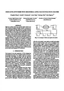
Figure 1. Simulation of the Fetch cycle and Execute cycle of the instruction LDAA with extended addressing.
We will disregard any propagation delays since this is a behavioral model. The first clock cycle of all instructions will fetch the op-code from memory and latch this information into the instruction register (ir). The natural simulation of this cycle is:
It is quite difficult to behaviorally model all of the instructions of the 68HC 1 1 with blocking assignments because of these timing problems. With the data structure described below, the correct simulation is easier to obtain. We need a way to hold information temporarily and then transfer that information into its proper destination at the rising edge of the next clock cycle. The data structure that we developed allows us to transfer information at the correct time without complex coding. The data structure contains two parts, .old and .new. At each positive edge of the clock cycle, this data structure transfers the .new value to the .old. This allows another process to change the .new during the clock cycle, and have these changes take effect in the .old at the next rising edge of the clock. It is possible to do this because Verilog allows the definition of modules that will group information together [ 5 ] . In addition to simply defining a module that will group the .old and .new information together, we define an always block that waits until the positive edge of the clock. It then assigns .old the value of .new.
--place the pc on the address bus --place the contents of the addressed memory on the data bus --increment the pc --latch the data bus into the ir --wait for the positive edge of the clock. Simple code for this cycle (similar to [2]) using blocking assignments follows. While it is algorithmically correct, it allows information to be latched into registers at the incorrect time as is shown in figure 1.
a (posedge
sysclk) addr = pc; data = mem[addrl ; pc = pc+l; ir = data; @ (posedge sysclk)
module register(c1ock); parameter SIZE = 1; input clock; reg [SIZE - 1:0] new,old;
The timing in figure 1 is incorrect because Verilog will treat the statements preceding the second aposedge as though they occur simultaneously. For the contents to be in the ir at the beginning of this clock cycle implies that the memory has an instantaneous access time. To model the data transfers so that they take effect during the correct cycle, we need to place some statements after the second @posedge. (posedge addr data @ (posedge pc = ir = @
sysclk) pc; mem[addrl sysclk) pc + 1; data; = =
initial old = 0; initial new = 0 ; always @(posedge clock) old = new; endmo du 1e
We can think of this module definition as a traditional software data structure (i.e., a struct in C ) . In fact, becailse of Verilog’s ability to combine such data with a unique procedural instance, it has some of the aspects of a class definition in C++.
;
102
(t) is introduced in our model. The code for the naive approach is:
Let us simulate the fetch cycle using our technique. The busses are defined with reg, but pc, ir and acca are defined with our register. We place the pc.old on the address bus, the contents of memory pointed to by the address bus onto the data bus, pc.old+l into pc.new, and move the value of the data bus into ir.new. At the next rising edge of the clock, the updated values will be clocked into the .old parts of the variables. The following correctly models the op-code fetch cycle using our method:
//CYCLE 2 (posedge sysclk) addr=pc ; data=mem [addr] ; pc=pc+l ; t={data,t .old [7 : 01 } @
;
//CYCLE 3 (posedge sysclk) addr=pc ; da ta=mem [ addr 1 ; pc={t .old [15:71 ,data}; @ (posedge sysclk) @
(posedge sysclk) addr = pc.old; data = memraddrl ; pc.new = pc.old+l; ir.new = data; @ (posedge sysclk) @
Figure 3 shows several things wrong with the naive simulation of this instruction. Clock cycle 3 shows an interesting contradiction. It is incorrect to have the lower eight bits of the effective address on the data bus and the effective address in the pc simultaneously. It would be very difficult to use naive blocking assignments to simulate this properly because the next clock cycle fetches the next instruction.
Figure 2 shows a graph of the fetch (and execute) of LDAA which matches the description in [7]. Our technique solves the problem of using blocking assignment statements to correctly model synchronous register transfers. For example, the op-code for LDAA direct (S’h96) is present in the ir during, but not before, cycle 2 unlike figure 1 .
d
n
1
nU nL
xooo5
I0002 0005
Figure 3. Simulation of JMP instruction using extended addressing modeled with the naive approach.
Figure 2. Simulation of the LDAA instruction using the .old and .new data structure.
By using our approach, we can easily solve all of these problems because the transfer of data takes place when entering the fetch cycle. The following code segment uses our approach to model cycles two and three of the instruction. Figure 4 shows the timing diagram obtained with this code segment. Our approach easily avoids the problem of data being clocked into its destination a clock cycle too early. This allows data transfers to be initiated during the appropriate clock cycle and take effect at the rising edge of the next clock cycle, the code closely resembles that of the naive approach. Yet figure 4 illustrates that our technique produces a timing diagram that matches the actual operation.
JMP Instruction with Extended Addressing The cycle by cycle operations [7] of the JMP instruction are: Cycle 1 2 3
Address OP OP+ 1 OP+2
Data 7e hh 11
To naively simulate this instruction with blocking assignment statements, we fetch the op-code as previously described and then fetch the two portions of the effective address. To hold this address, a 16 bit temporary register
103
(3 (posedge
sysclk) addr=pc.old; data=mem [addrl ; pc.new=pc.old+l; t .new={data,t .old[7 :03 } ; @ (posedge sysclk) addr=pc.old; data=mem [addrl ; pc.new={t.old[l5:8],data};
Comparison with non-blocking assignment By using non-blocking assignment statements (O; i = i - I ) s[i] = s[i-I]; endmodule
module main; wire sysclk; register #16 pc(sysc1k); register #8 t(sysc1k); register #8 acca(sysc1k); pipeline #(8,2) ir(sysclk); pipeline #( 1,3) is-opcode(sysc1k); cl clock(sysc1k); reg [7:0] datal,data2; reg [ 15:0] addrl ,addr2; reg [7:0] mem[4095:0]; initial begin in it-mem; # 1 ispopcode.s[O] end
=
1;
always begin @(posedge sysclk) #1 addrl = pc.old; datal = mem[addrl]; addr2 = t.old;
107