optically-coupled monostable. ... regulator, a multivibrator, a photocoupler, a switching circuit .... pulse duration of the load current is imposed by a monostable.
Proceedings – 23rd Annual Conference – IEEE/EMBS Oct.25-28, 2001, Istanbul, TURKEY
A Simple Constant-Current Neural Stimulator With Accurate Pulse-Amplitude Control J. A De Lima & A. S. Cordeiro VLSI & Instrumentation Group, Electrical Engineering Department, Universidade Estadual Paulista 12516-410 Guaratinguetá-SP - Brazil
Abstract: A simple constant-current electrocutaneous stimulator for high-impedance loads using low-cost, standard high-voltage components is presented. A voltage-regulator powers an oscillator built across the primary of a transformer whose secondary delivers, after rectification, the high-voltage supply to switched current-mirrors in the driving stage. Since the compliance highvoltage is proportional to the stimulation current, overall power consumption is minimized. By adjusting the regulated voltage, control of the pulsed-current amplitude is achieved. A prototype with readily available components features stimulation currents of amplitude and pulsewidth in the range 0≤ ≤Iskin≤20mA and 50µs ≤Tpulse≤1ms, respectively. Pulse-repetition spans from 1Hz to 10Hz. Worst-case ripple is 3.7% @Iskin=1mA. Measured pulse fall-time is shorter than 32µs. Overall consumption is 4.4W @Iskin=20mA. Subject isolation from power line is 4KV. I. INTRODUCTION
Electrical stimulators represent a class of medical electronic devices that are useful either therapeutically as prostheses [13]. They have been powerful tools to restoring partial functionality to neurologically damaged individuals while providing a medical diagnostic of the nervous system. Stimulation that innervates the muscles can be used in physical therapy to regain some degree of muscular control. Functional Electric-Stimulation (FES) systems are mainly useful in cases dealing with temporary paralysis caused by atrophy of the muscle owing to disuse that considerably reduces its mass. By means of a periodic direct stimulation, the clinician can exercise the damaged muscle, even though normal neurostimulation is not available. Additionally, programmed electrical-stimulation can be used to enhance function of paralyzed muscles resulted from neurological injury. Stimuli parameters vary widely according to the type of muscle stimulation, the number of channels, the type of electrodes and the specified safety-factor. Many commercially available stimulators deliver voltage pulses and require additional features to monitor and set up the current level as it changes with the electrode/skin load-characteristic. Constantcurrent stimulators are therefore mostly indicated since the charge transferred per stimulus is constant regardless the load impedance. On the current-pump stimulator reported by Poletto et al. [4], the voltage-to-current (V/I) converter requires opamps with a particular combination of high-voltage tolerance and large slew-rates while demanding special care for frequency compensation and over-voltage/current protection. Its output stage uses five power-supply modules so that a power-up management circuit is needed to establish the appropriate turn-on sequence of these supplies. On the approach proposed by Kaczmarek et al. [5] , the V/I conversion requires a fixed-value high-voltage supply, regardless the This work was partially supported by Neurotec®, CP 98, 37500-000, ItajubáIEEE MG,0-7803-7211-5/01$10.00©2001 Brazil.
amplitude of the stimulation current. In this case, additional circuitry would be necessary to minimize safety hazardous and stand-by power consumption. This work describes an alternative and simple constantcurrent stimulator employing only conventional high-voltage components while featuring good controllability of stimulation parameters such as amplitude, duration and frequency of the pulsed-current. Its small number of components makes it attractive for low-cost applications. Basically, a voltageregulator powers an oscillator built around the primary of an elevator transformer whose secondary delivers, after rectification, the necessary compliance voltage to a switched V/I converter in the driving stage. Furthermore, subject isolation from the power line is naturally achieved. Accurate amplitude-control of the load current is performed in the voltage-regulator, whereas pulsewidth is controlled by an optically-coupled monostable. In contrast with [5], the highvoltage supplied to the V/I converter has its value proportional to the stimulation current, reducing thus power consumption and improving safety protection. Although originally devised to stimulate muscles through the skin, the proposed topology can be extended to other ranges of neural stimulators. The paper outline is as follows. Section II describes the proposed stimulator topology and schematic, whose design is discussed in Section III. Experimental results are presented in Section IV. Concluding remarks are summarized in Section V. II. DESCRIPTION OF THE NEURAL STIMULATOR
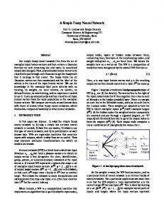
The block diagram of the proposed neurostimulator is displayed in Figure 1. It consists of a pair of transformers followed by full-bridge rectifiers, an adjustable voltageregulator, a multivibrator, a photocoupler, a switching circuit and a V/I converter in the driving stage. The load represents both resistive and reactive components of the electrode/skin interface as well as the bulk tissue resistance. Specified intervals for the amplitude and pulsewidth of the stimulation current are 0≤Iskin≤20mA and 50µs≤Tpulse≤1ms, respectively. The ripple associated with Iskin is limited to 6%. Pulse-repetition ranges from 1Hz to 10Hz. T1
T2 Voltage Regulator
Astable
127V AC 60Hz Load
V/I Converter
External Trigger
One-shot Generator
Switching Circuit
Figure 1. Block diagram of the neurostimulator
Report Documentation Page Report Date 25OCT2001
Report Type N/A
Title and Subtitle A Simple Constant-Current Neural Stimulator With Accurate Pulse-Amplitude Control
Dates Covered (from... to) Contract Number Grant Number Program Element Number
Author(s)
Project Number Task Number Work Unit Number
Performing Organization Name(s) and Address(es) VLSI & Instrumentation Group, Electrical Engineering Department, Universidade Estadual Paulista 12516-410 Guaratinguetá-SP - Brazil
Performing Organization Report Number
Sponsoring/Monitoring Agency Name(s) and Address(es) US Army Research Development & Standardization Group (UK) PSC 803 Box 15 FPO AE 09499-1500
Sponsor/Monitor’s Acronym(s) Sponsor/Monitor’s Report Number(s)
Distribution/Availability Statement Approved for public release, distribution unlimited Supplementary Notes Papers from the 23rd Annual International conference of the IEEE Engineering in Medicine and Biology Society, October 25-28, 2001, held in Istanbul, Turkey. See also ADM001351 for entire conference on cd-rom. Abstract Subject Terms Report Classification unclassified
Classification of this page unclassified
Classification of Abstract unclassified
Limitation of Abstract UU
Number of Pages 4
Proceedings – 23rd Annual Conference – IEEE/EMBS Oct.25-28, 2001, Istanbul, TURKEY
The circuit operation is now briefly described. Line transformer T1 steps the 60Hz mains-voltage down to 30VAC. Following a four-diode bridge and a bulk-capacitor filter, the rectified voltage is input to a regulator circuit, whose output is adjustable within the interval 0-12V and sets the supply voltage to the astable. Since such a circuit is loaded by the primary of the elevator-transformer T2, the oscillation across the secondary attains high-voltage amplitudes and provides the necessary compliance voltage to generate the desired stimulation currents. As function of the regulated voltage, the peak-amplitude at the secondary of T2 varies from 0 to 220V. After a second full-bridge rectifier, a high-voltage supply is available to a switched V/I converter built upon cascode current mirrors that delivers to the load a constant-amplitude pulsed-current. Pulse duration is externally set up by a monostable and triggered by a TTL-level signal. The resulting one-shot pulse is delivered to a photocoupler that drives a switching circuit made up of discrete transistors. For explanatory reasons, the neurostimulator schematic is split into three main elements: the oscillator, the output V/I converter and the switching circuit. These parts are discussed below in more details.
on the current mirror, so that a pulsed current is delivered by the stage. 127VAC 60Hz
B. Voltage-to-Current Converter Figure 3 shows the schematic of the driving stage, built around a self-biased current-mirror formed by MOS transistors M1–M4. The standard cascode configuration was chosen by its simplicity while providing a high dynamic output-resistance [6]. All transistors are N-channel devices (MPT2N60). RE and CE are the reactive components of the electrode/skin interface and Rskin is the tissue resistance. Fixing R5 and denoting VDDO=VDDO+-VDDO-, it comes out Iskin=(VDDO-VGS1-VGS3)/R5. VDDO determines then the current through the skin, which is independent of the load characteristic, at good approximation. Adjusting Iskin by means of R2 in the voltage-regulator compensates for the poor matching between discrete transistors in the current mirror. Upon assertion of phase Φ1, M5 switches
D1
D2
R1
C1
D5
D6 D7 D8
~
D3
6:1
R2
D4
Q1
T2
VDDO +
VOS+
D10
D11
VR
C6 C5
C3
D9
C2
R3
C4
C7 D13
D12
R4 1:15 VOS
VDDO-
Q2 Figure 2. Oscillator schematic VDDO +
A. Controlled-Amplitude Oscillator The oscillator schematic is illustrated in Figure 2. T1 is a transformer with a ratio of windings N1=1:6 and lowers the power-line voltage from 127VAC rms to 30Vpeak. Following a full-bridge rectifier with diodes D1–D4 (1N4007) and filtercapacitor C1, the rectified voltage is input to a voltageregulator (LM317T), whose output VR’≅1.25(1+R2/R1)[V] is tunable within 1.25V-30V. Ultimately, the magnitude of the stimulation current is proportional to the regulated voltage, which can be adjusted by potentiometer R2 in the present prototype. Nevertheless, advanced versions may feature a programmable adjustment, by means of a D/A output of a microcontroller, for instance. Diodes D5-D6 (1N4007) produce the voltage drop that ensures 0V as the minimum dc-voltage VR supplied to a multivibrator astable, which comprises bipolar transistors Q1-Q2 (TIP41C), base resistors R3-R4 and collectorcoupling capacitors C4-C5. Since oscillation is developed across the center-taped primary of transformer T2, which has a ratio of windings N2=1:15, a high-voltage oscillation appears at its secondary. Supply-voltages VDDO+ and VDDO- are available after a dc-conversion by the bridge D10-D13 (1N4007) and C7.
VR'
LM317
T1
I SKIN CE
RE
R5
RS
Φ1 -
M3
M4
M1
M2
M5
VDDO
Figure 3. Schematic of the driving stage
C. Timing and Switching Circuit Figure 4 shows the timing and switching circuit, comprising a photocoupler (4N25), which electrically isolates the stimulator from the external circuitry that imposes the pulse duration, and a push-pull driver. On the present prototype, the pulse duration of the load current is imposed by a monostable formed by Q3-Q4 (BC547), Q5 (TIP41), Q6 (TIP42), R7-R11 and C8-C9, and triggered by a TTL-level signal VTR. The one-shot pulse is then input to the optocoupler. High-voltage control phase Φ1 is available at the push-pull (TIP41, TIP42) output. VDDO +
V DC R9
R 10
R 11 Q5
Φ1
Q4 C9
VTR
Q3 C8
R8
Q6 R 12
R7 VDDO-
Figure 4. One-shot generator and switching circuit
Proceedings – 23rd Annual Conference – IEEE/EMBS Oct.25-28, 2001, Istanbul, TURKEY
Considering the use of electrodes with small surface areas, a maximum value of 10KΩ was assumed for the highly nonlinear resistance Rskin that mimics the electrode/skin interface and the bulk resistance [4,7]. Adopting R5=10KΩ and accounting for voltage drops VDSAT2, VDSAT4 and VDS5 in the driving stage, a compliance voltage VDDO=210V assures proper current mirroring at maximum 20mA-load current. As a result, the amplitude of the oscillation to be developed across the secondary of T2 should reach 420Vpp, which imposes 1V≤VR≤14V as the operation range to the voltage-regulator. It is worth noticing that VR=0 entails Iskin=0. The design requirements on sizing filter-capacitor C7 are twofold: i) the minimum energy per a pulsed stimulus and ii) the highest allowed ripple on Iskin. Neglecting the consumption dissipated by the current-mirror transistors, the energy to be delivered by C7 is Etot≅2RskinIskin2Tpulse+Eopt, where Eopt is the optocoupler component. Straightforward manipulation leads to C7≥2(2+η)Tpulse/Rskin, where η=Iopto/Iskin and Iopto is the current delivered by the optocoupler. C7 should thus be sized in accordance with the largest pulsewidth and smallest amplitude of Iskin. A preliminary characterization of Iopto as function of the stimulation current is displayed in Figure 5. Taking Tpulse=1ms and Iskin=1mA, it comes out C7≥1.33µF for Iopto=4.6mA.
Pulsewidth spans from 50µs to 1ms and can be adjusted by potentiometer R9 in the monostable. Other components are R7=1KΩ, R8=R10=10KΩ, R11=1KΩ and C8=C9=1µF. IV. EXPERIMENTAL RESULTS
A wire-wrapped prototype of the neurostimulator was implemented. Heat sinks were properly attached to the voltageregulator and the optocoupler. Both transformers T1 (15VA) and T2 (3VA) provide a minimum 4KV-isolation. All resistors are 1/4W-carbon with 5%-tolerance. To appraise the stimulator limits without the restriction imposed by subject pain-threshold, a 10KΩ-load resistor Rskin was initially fixed. The measured transfer function of the circuit, defined as the amplitude of the load current against the regulated voltage, is shown in Figure 6, for stimulation rates of 1Hz and 10Hz. At maximum-current condition, the waveform of the oscillation at the secondary of T2 is shown in Figure 7. Amplitude and frequency are 438Vpp and 204Hz, respectively. 20 16
Iskin [mA]
III. CIRCUIT DESIGN
12 8
10 T pulse = 1ms
0
8
Iopto [mA]
f = 10Hz f = 1Hz
4
9
0
2
4
6
8
10
12
Regulated Voltage [V]
7
Figure 6. Measured amplitude of Iskin as function of regulated voltage
6 5 4 0
2
4
6
8
10
12
14
16
18
20
2
I skin [mA] Figure 5. Dependence of Iopto on the stimulation current
The ripple factor is given by [1-exp(-Tpulse/τ)], where τ =RLC7 and RL≅Rskin//R5//Ropto is the filter resistive-load. Ropto denotes the dc-resistance VDDO/Iopto of the optocoupler branch. Based on the measurements presented in Figure 5, one has 1.95KΩ≤RL≤4.1KΩ for the given range of VDDO and Iskin. Adopting C7=8.8µF, the calculated ripple for worst-case 1mspulsewidth is 5.66% @Iskin=1mA and 2.73% @Iskin=20mA. Larger values of C7 would decrease the ripple, at expense of higher overall consumption, as VR should be increased. Supposing that the astable generates a square waveform and approximating the analysis to the case of a purely resistiveload at the collector of Q1-Q2, the oscillation period is Ta≅2R3CXln[(VR-VBE)/(2VR+VBE-VCEsat)], where CX represents the series association of C4 and 0.5C6. Choosing R3=R4=10KΩ, C4=C5=0.47µF and C6=2.2µF, the oscillation-frequency interval is 170Hz≤fa≤199Hz. Setting such relatively low frequencies aims to reduce the oscillator power consumption, and consequently, the current supplied by the voltageregulator, while still complying with the specified ripple on the stimulation current.
Figure 7. Oscillation at T2 secondary at condition of Iskin=20mA
A volunteer subject was solicited after the ethical approval for the project was granted. Prior to stimulation, the skin of the subject’s wrist was abraded and an electrolyte gel applied to improve contact with the electrode leads. Tests were performed at different stimulation ratings. The waveforms of the voltage across R5 (a) and skin electrodes (b) at Iskin=20mA are shown in Figures 8 and 9, for Tpulse=50µs and Tpulse=1ms, respectively. Measured pulse transitions shorter than 32µs make the circuit suitable to relatively high stimulation rates. The relative peak-to-peak ripple on the pulsed current as function of the amplitude is shown in Figure 10, for C7=8.8pF and pulses 1ms-long. A maximum variation of 2.5% was found within the interval 4mA≤Iskin≤20mA, which is slightly lower
Proceedings – 23rd Annual Conference – IEEE/EMBS Oct.25-28, 2001, Istanbul, TURKEY
than the calculated values. As expected, ripple increases at lower Iskin values as τ =RLC7 follows the reduction of Ropto. The stimulator consumption is 4.4W @Iskin=20mA. A summary of measured parameters of the stimulator is listed in Table 1.
whereas the pulse duration is controlled by an opticallycoupled monostable circuit. A prototype employing readily available components exhibits stimulation currents of amplitude and pulsewidth in the interval 0≤Iskin≤20mA and 50µs≤Tpulse≤1ms, respectively. Stimulation rate is from 1Hz to 10Hz. The measured ripple is 3.7% @Iskin=1mA and 1.9% @Iskin=20mA. Total power consumption is 4.4W @Iskin=20mA. Subject isolation from power line is 4KV. Although the circuit is devised to electrocutaneous stimulation of muscles and designed for a maximum skinresistance of 10KΩ, the proposed topology can be applied to other ranges of stimulators. Its small number of components and low consumption make it valuable for low-cost and remote applications. The use of components with higher voltage specifications can accommodate larger values of stimulation current and skin resistance. TABLE 1
Figure 8. Voltage across skin electrodes at Iskin=20mA and Tpulse=50µs
NEUROSTIMULATOR MEASURED CHARACTERISTICS
Output Current (mA) Pulse Duration (µs) Fall Time (µs) Ripple (%) Stimulation Rate (Hz) Consumption (W)
Min 0 50 1.9 1 2.7
Max 20 1000 32 3.7 10 4.4
ACKNOWLEDGMENTS
The authors would like to acknowledge the fruitful discussions with the application engineers at Neurotec® and thank H. Bendinelli for her assistance during the development. REFERENCES
Figure 9. Voltage across skin electrodes at Iskin=20mA and Tpulse=1ms 4.0 3.5
Tpulse = 1ms
ripple [%]
3.0 2.5 2.0 1.5 1.0 0.5 0.0 0
2
4
6
8
10
12
14
16
18
20
22
Iskin [mA]
Figure 10. Measured ripple on stimulation-current as function of amplitude
V. CONCLUSION
A constant-current neurostimulator based upon standard high-voltage components was presented. It basically comprises a voltage-regulator that powers an oscillator built around the primary of a transformer. The secondary supplies, after rectification, the high-voltage to a switched current-mirror in the output driving stage. Since the compliance high-voltage is proportional to the stimulation current, consumption is reduced, which is attractive for battery-operated applications. The current amplitude is adjusted by the regulated voltage,
[1] Medical Instrumentation: Application and Design, edited by Webster, J. G., 3rd Edition, John Wiley & Sons, 1998. [2] Peckham, P. H. – “Functional Electrical Simulation”, Encyclopedia of Medical Devices and Instrumentation, edited by Webster, J. G., pp. 1331-1352, John Wiley & Sons, 1988. [3] Gudnason, G., Bruun, E. & Haugland, M. – “An Implantable Mixed Analog/Digital Neural Stimulator Circuit”, Proc. of ISCAS99, Orlando, USA, pp. V.375 – V.378, 1999. [4] Poletto, C. & Van Doren, C. – “A High Voltage, Constant Current Stimulator for Electrocutaneous Stimulation Through Small Electrodes”, IEEE Trans. on Biomedical Engineering, Vol. 46, No. 8, Aug. 1999. [5] Kaczmarek, K., Kramer, K., Webster, J. & Radwin, R. – “A 16-Channel 8-Parameter Waveform Electrotactile Stimulation System”, IEEE Trans. on Biomedical Engineering, Vol. 38, No. 10, Oct. 1991. [6] Johns, D. & Martin, K. – “Analog Integrated Circuit Design”, John Wiley & Sons, 1997. [7] “Neurostimulator Characteristics”, Internal Report #27/00, Neurotec.