the interface signals (voltage, current for analog pins and logic level for digital pins). (2) Mode sequence charts are
A Static Verification Approach for Architectural Integration of Mixed Signal Integrated Circuits R. Mukhopadhyay a,∗, A. Komuravelli a, P. Dasgupta a S. K. Panda a, S. Mukhopadhyay b a Dept. b Dept.
of Computer Science and Engg., Indian Institute of Technology, Kharagpur, India
of Electrical Engg., Indian Institute of Technology, Kharagpur, India
Abstract In this paper we present a static method for verifying the proper integration of analog and mixed signal macro blocks into an integrated circuit. We consider the problem in a setting where there is no golden reference for verifying the validity of the interconnections between the blocks. The proposed verification methodology relies on an abstract modeling of the functional behavior of the blocks and a set of consistency criteria defined over the composition of these abstract models. A new formalism called Mode Sequence Chart (MSeqC) has been presented for capturing the behavior of the blocks at a level of abstraction that is suitable for interconnection verification. We present rules to compose the MSeqCs of each block in an integrated design and present three criteria that indicate possible interconnection faults. We present a tool called AMS-IV (AMS-interconnection verification) that takes the design netlist as input, the MSeqC model of each design block as reference, and tests the three criteria. Key words: Static Verification, Design Integration, Mixed Signal Circuit, formal model.
1
Introduction
As designers attempt to integrate multiple pre-designed and pre-verified design blocks into an integrated circuit, the task of verifying that the integration has been done correctly ∗ Corresponding Author. Email address:
[email protected] (R. Mukhopadhyay).
Preprint submitted to Elsevier
has become a major challenge. The problem becomes significantly more complex when the component blocks are mixed-signal in nature, since mixed-signal simulation is prohibitively complex as compared to pure digital simulation. In this paper we study the verification problem associated with integrating several complex mixed-signal circuit blocks into an integrated circuit. We have been studying this problem in the context of integrating power management units (PMUs) for portable devices, such as cell phones, PDAs and laptops. A typical PMU contains several linear drop out regulators (LDOs), a few buck regulators, a battery charger and several other blocks for bias generation, UVLO, etc, and digital control. Typically the manufacturers of such PMUs have existing design IPs for these components, and the main challenge is to integrate a combination of these components (as required by the customer) into an integrated PMU within very low time budget. The whole design fails if the components are not interconnected correctly, where interconnection (in the analog sense) also refers to proper polarity, drive strength, etc. We require a functional specification as a reference in this verification problem, even if the goal is only to verify that the interconnections have been made correctly. This is due to the fact that there is a manual point of entry for the interconnections. There are broadly two practices for integrating multiple mixed-signal circuit blocks into an integrated chip. The most common form is to make the interconnections graphically using a schematic editor (such as Cadence Virtuoso Schematic Editor [26]). The other approach attempts to enter the interconnections textually, either directly using text formats (using HDLS such as Verilog[24], VerilogA [25] etc.) or indirectly using scripting languages. In both approaches the point of entry is human and therefore prone to similar types of errors. Therefore integration verification is not achievable without functional verification of the integrated design. Formal verification methods for AMS designs based on equivalence checking [2, 15, 23], model checking [14, 10, 3, 16], theorem-proving [8, 12, 11] etc. do not address the problem of verifying integration of large integrated AMS designs. On the other hand run-time verification methods such as [4, 19, 17] require simulation of the integrated AMS design. Typically the integrated designs that we refer to are so large that adequate functional verification through mixed-signal simulation of the integrated netlist is infeasible in practice, as also observed by the author of [22]. At the same time the full functionality of the component blocks is typically not required for verifying the correctness of the integration. For example, it is possible to replace the component blocks with lightweight behavioral models and ramp up the simulation speed of the integrated design. In a related work we adopted this approach using Verilog A [25] models with reasonable success. Based on our experience, we have the following observations: (1) Developing Verilog A models for complex blocks like buck regulators is non-trivial. It is possibly too much of an effort to develop executable behavioral models for all legacy designs of the components. (2) Verilog A models are not suitable for static (formal) analysis. We believe that most interconnection errors can be detected statically against a well defined functional specification. 2
(3) The industry seems to be moving towards platform based design methodologies where third party design IPs are integrated at the physical level (post layout). It is unlikely that behavioral models for such components will be made available. In this paper we present a new formalism, called mode sequence charts (MSeqC), for modeling the component blocks of an integrated circuit at a very high level of abstraction. There exists a number of formalisms to specify components of a system at various levels of abstractions. In [6] an automata based language for specifying software components have been proposed. An extension of hybrid automata [1] to model interaction among various hybrid systems is proposed in [18]. StateCharts [13], which is another formalism to model complex systems is based on extension of state machine models. Message Sequence Chart [20] is a graphical and textual language for specifying interaction among various communicating system components. Although our model is not the first model that attempts to capture the interaction among various interacting components (which are mixed signal circuits in our case) mode sequence chart captures a circuit specification exactly at the level of abstraction that is appropriate for carrying out our interconnection verification method. A mode sequence chart captures the macro modes at which a mixed signal block works, and the admissible transitions between these modes. Each state of the chart is annotated with a set of assumptions that are made about the environment when the component is in that mode, and a set of properties that the component guarantees while operating in that mode. There are several advantages of using this formalism for the verification problem addressed in this paper. (1) Mode sequence chart is a very simple formalism as compared to existing formalisms for hybrid systems (such as hybrid automata [1], hybrid petri net [5]). It abstracts out the dynamics of a circuit at a particular mode of operation as a set of linear constraints over the interface signals (voltage, current for analog pins and logic level for digital pins). (2) Mode sequence charts are amenable for static (formal) analysis in integration verification. (3) Mode sequence charts can typically be developed from the specs of the block that it models. It is therefore quite useful for modeling third party design IPs for which adequate functional details are unavailable. Each global state of the integrated circuit is a composition of compatible states of the mode sequence charts of the components. Interconnection errors manifest themselves in terms of incompatibility of local states corresponding to a desired global state, and in terms of unreachability of desired global states. The main contributions of this paper are as follows: (1) We introduce mode sequence charts as a high level formalism to be used in interconnection verification. (2) We present the composition rules for integrating the mode sequence charts of the components based on the interconnections entered by the designer in the schematic. (3) We present three different formal criteria for verifying the correctness of the interconnections. Interconnection errors are typically manifested in terms of violations of these criteria. 3
(4) We have developed a tool called Analog and Mixed Signal Interconnection Verifier (AMS-IV) Tool that essentially checks the three criteria and produce three corresponding reports. These reports are useful to determine whether the circuit has any interconnection fault. In the next section we illustrate our basic idea of interconnection verification with a toy example. Section 3 formally presents mode sequence chart and Section 4 describes the interconnection model. In Section 5 we propose three interconnection fault detection criteria and explain them with examples. Section 6 presents the algorithm and implementation of the AMS-IV tool briefly. In Section 7 we present a case study on a voltage mode buck regulator circuit. Section 8 concludes the paper with a few possible topics for future research.
2
Basic Idea
This section illustrates the basic idea of our method of interconnection verification with a toy example. Example 1 Consider a switched capacitor integrator of Figure 1. Sreset
Csum Sin:sig
Cin
Sout:sig
Vin
VDD − +
Sin:gnd
Vout
Sout:gnd
Fig. 1. A switched capacitor integrator circuit [21]
The input voltage Vin is fed to the operational amplifier through the input capacitor Cin . The circuit works in two phases. In the first phase the Sin:sig and Sout:gnd switches are closed, and Sreset , Sin:gnd, and Sout:sig are kept open, thus charging Cin . This is called the sampling phase. In the next phase, called the update phase, Sin:gnd and Sout:sig are closed and Sreset , Sin:sig , and Sout:gnd are kept open, thereby charging Csum . In this phase the charge accumulated on Cin in the sample phase is passed onto Csum thus changing the output voltage. It can be shown that for an ideal switched capacitor integrator
Vout:i = Vout:i−1 + Vin:i(Cin /Csum )
(1) 4
where Vout:i is the output voltage at the ith update phase. A correct operation of the circuit requires correct inputs from the environment. If the switches are not closed and opened in the proper order, the switched capacitor integrator cannot operate properly. A mode sequence chart of the integrator circuit captures this requirement through admissible state transitions. Figure 3 shows a switched capacitor integrator circuit connected with a hypothetical controller. The mode sequence chart of both the modules are also shown. The boxes represent the states of the circuits. Figure 2 shows the basic structure of such a box, that we use throughout the paper to represent state or mode of a circuit. We call such a box the mode template. Name of the mode Assume Constraints 1. A1 2. A2 . . n. An
Guarantee Constraints 1. G1 2. G2 . . n. Gn
Fig. 2. The Mode Template
There are three sections of a mode template. The top section is used to mention the name of the mode. The second and third sections are used to mention the list of assume and guarantee constraints of the mode. The constraints are presented in the form of a list. Each item of the list need to be ANDed to obtain the overall constraint. For example, in Figure 2 the overall assume constraint is A1 &&A2 ..&&An and the overall guarantee constraint is G1 &&G2 ..&&Gn . Note that an item viz. A1 can contain logical ORs. In Figure 3, the directed edges represent admissible state transitions. The constraints mentioned in each state are the assumptions and guarantees over the environment at that state. For example, the assumption of the integrator circuit on its interface pins at OF F state is that Sreset is high. Similarly at the OF F 0 state the guarantee of the controller on its sd pin is given as sd i.e. sd is high. Only assumptions of integrator circuit and guarantees of the controller are mentioned in the figure. Observe that in the mode sequence chart of the integrator circuit there is no edge between the OFF state (the initial reset condition of the circuit) and the UPDATE state. This correctly models the specification that the integrator circuit should not go to the update phase from the initial reset condition. The connections shown in the figure are correct. If by mistake, pin a is connected with pin Sin:gnd , pin b with pin Sin:sig , pin c with pin Sout:sig and pin d with pin Sout:gnd the integrator circuit will fail to operate properly. This is because in presence of these wrong connections when the controller makes a state transition from its initial state to sampling state, a and c become high and b and d remain low. This in turn makes Sin:gnd and Sout:sig high and Sin:sig and Sout:gnd low. When Sin:gnd and Sout:sig are high the integrator circuit should be 5
PWRP
PWRP SAMPLE0
SAMPLE Assume Constraints
Assume Constraints
Guarantee Constraints
1. sd 2. a 3. b 4. c 5. d
OFF0 Assume Constraints
sd
Guarantee Constraints
1. sd 2. a 3. b 4. c 5. d
Sreset OFF0
a
Sin:sig
Guarantee Constraints
b
Sin:gnd
c
Sout:gnd
d
Sout:sig
1. Sreset
vout Guarantee Constraints
UPDATE Assume Constraints
1. 2. 3. 4. 5.
Guarantee Constraints
1. 2. 3. 4. 5.
Sreset Sin:sig Sin:gnd Sout:gnd Sout:sig
Assume Constraints
UPDATE0 Assume Constraints
1. 2. 3. 4. 5.
sd a b c d
Sreset Sin:sig Sin:gnd Sout:gnd Sout:sig
Guarantee Constraints vin
PWRN
PWRN
Fig. 3. A switched capacitor integrator with a digital controller
in its update state. But, it cannot move to the update state from its initial reset state as this transition is prohibited being an illegal transition. Similarly, it can be verified that the integrator circuit cannot transit to update state because of these wrong connections. Thus the integrator circuit can neither transit to SAMP LE or UP DAT E state because of the mentioned wrong connections. In other words, both the SAMP LE and UP DAT E states of the integrator are unreachable due to the wrong connection. 2
3
Mode Sequence Chart (MSeqC)
In the absence of any reference for the correct integration of a set of pre-designed and preverified blocks into an integrated circuit, verification of the integration can be done in two broad ways, namely: (1) Verify the functionality of the integrated design against the specification of the integrated circuit (2) Check for inherent inconsistencies in the integrated design The first task is expensive and often the verification coverage is low for large integrated circuits. Moreover, the specification of the functionality of the integrated circuit does not define the correct interconnection between the blocks, rather the correct interconnection leads to the satisfaction of the specification. On the other hand, interconnection errors between blocks in mixed-signal designs almost always lead to inherent inconsistencies in the integrated design, which can be detected early without knowing the functionality of the integrated design. The beauty of this approach 6
lies in choosing a level of abstraction for specifying the functionality of the blocks. We shall show that many, if not most, of the interconnection errors manifest themselves as inherent inconsistencies if we use simple models of the blocks which capture the macro modes in which these blocks function. Analog and mixed-signal circuits typically function in a set of operating modes. For example a voltage amplifier typically works in two distinct operating modes: OFF and LINEAR, where OFF represents the cutoff state of the amplifier and LINEAR represents its normal amplifying mode of operation. In each of these operating modes there are various assumptions and guarantees on the voltage and current values of its interface pins. It is quite easy for a designer to specify the operating modes of a design block and to enumerate the assumptions and guarantees in each operating mode. For example, design specifications of a voltage amplifier routinely contain information like input common mode voltage range VICM R , input voltage range VI etc., which specify assumptions about the signals at the non-inverting and inverting pins. These assumptions are constraints in terms of the voltage at the inverting and non-inverting pins, which are to be guaranteed by the circuits interfacing with the amplifier to drive the amplifier into its linear mode of operation. Similarly, there are assumptions on input bias current, output load current of the amplifier etc. Mode Sequence Charts (MSeqC) are simple finite state models of design blocks, where the states capture the macro modes of operation of a block and a state is annotated with the set of assumptions and guarantees that are expected when that block operates in that mode. We will show that many interconnection errors manifest themselves in the form of the following types of inconsistencies in the integrated design, when the blocks are modeled as MSeqCs. The integrated design model is obtained by a parallel composition of the MSeqCs of the blocks. (1) A reachable state of one MSeqC becomes unreachable in the integrated design model. (2) In a reachable state of the integrated design model, the assumptions required by one MSeqC is not guaranteed by the others. (3) The set of reachable states of the integrated design model does not cover all the specified reachable states (given separately). Also, we consider the case where the set of reachable states of the integrated design model contains one or more undesirable states (also given separately). Our experience shows that the three criteria stated above cover most of the typical interconnection errors at the architectural level of large mixed signal integrated circuits. The formal definitions follow. The specification S of a block M is represented by a mode sequence chart, which is a tuple J =< S, s, τ, Z, A, L, PA, PG > where • S: set of discrete modes/states of the circuit block. • s: initial state. 7
• • • • • •
τ ⊆ S × S: transition relation between states. Z: set of interface signals of the block. A: set of attributes, namely, {T Y P E, NAT URE, P RIM SIGNAL, SHAP E} L : S × Z × A → value where value is defined as in Table 1 PA : set of mode/state specific assumptions. PG : set of mode specific guarantees.
Table 1 Attribute functions and possible values Attribute Functions
Range of Values
Meaning
TYPE
input, output, inout
It is the polarity of the pins.
NATURE
analog, digital
It is used to label the nature of the signal of the signal at the interface pin.
PRIM SIGNAL
voltage, current
This is used to define the primary signal at a pin. For example, voltage is the primary signal at the output pin of a voltage amplifier, current is the primary signal at the output pin of a current bias block.
SHAPE
sinusoidal, ramp, square, sawtooth, steady, random
This is used to describe the signal shape of the primary signal at a pin. Random refers to no specific signal shape.
Z consists of two types of signals: • ZA : set of analog/electrical signals. • ZB : set of Boolean signals. L is a labelling function that allows us to specify some of the important attributes of the interface pins at every state. This is important, as the attributes of a pin may vary from state to state. For example, a controllable signal generator which produces a sawtooth wave in one state might produce a sinusoidal signal in another mode of operation. Table 1 shows the list of attribute functions and their meaning. For a Boolean signal p ∈ ZB voltage is the only important signal. p represents logic high at p and ¬p denotes logic low. In the following section we use q to denote electrical/analog signals, and p to denote Boolean signals. The syntax of the properties in PA and PG are defined by the symbol PROP in the following grammar. The symbols && and || are used to denote the usual logical AND and OR opera8
tors repsectively. • • • • • •
PROP −→ PROP | B | PROP && PROP | PROP || PROP CONS −→ TERM REL TERM | CONS || CONS B −→ B || B | ¬B | p where p∈ ZB TERM −→ TERM OP TERM | v(q) | i(q) | f (q) | CONSTANT where CONSTANT ∈ R REL −→ > | ≥ | < | ≤ | = OP −→ + | - | * | /
The meaning of the analog terms are as follows. • v(q) : The voltage at q with respect to some reference node/ground • i(q) : The current through q out of the module. • f (q) : Frequency of the primary signal at pin q. This can be used to specify a range of values e.g. 10K < f (q) < 1M or a constant value f (q) = 10K (for example a sinusoidal signal has constant frequency). 3.1 Example of Modeling Specification with Mode Sequence Chart An essential module of any portable power management unit (PMU) is a battery charger. Fig 4 shows the block diagram of a battery charger, connected to a battery. A battery charger is a mixed signal circuit consisting of a digital controller and an analog driver circuit. The digital controller, which determines the mode of operation of the analog circuit, is a state machine whose state transitions are triggered by events from the analog part, that are defined over the voltage (Vbattery ) and current (Icharger ). Depending on the state, termed fsm state, of the digital controller the charging voltage Vbattery and the charging current Icharger are set by the battery charger. C
I charger
Battery Charger
Digital Controller
B
Analog Circuits
V battery
Fig. 4. Block Diagram of a Battery Charger
Fig 5 shows a typical charging profile of a battery charger. The charging profile consists of several distinct regions each of which corresponds to a distinct state of the battery charger. These are OFF, precharge, constant current, constant voltage, maintenance and ldo mode. A brief desription of these modes are given below. 9
Battery Voltage / Charge Current
I full
Vfull Battery Voltage Vdischarge
Vthreshold
Charge Current
I cutoff
I low Time
Fig. 5. Charging Profile for the Charger
• OFF Mode: If the external power supply is not within its specified range, disabled (i.e. the enable signal is not asserted) it enters this mode of operation. • Precharge Mode: In this mode, a constant current (say, 50 mA) is used to charge up the battery. The battery voltage increases with time in this state. • Constant Current Mode: As the battery voltage crosses a predefined threshold (say, 3 V) the charger enters constant current mode, where fullrate current i.e. the maximum rated charging current is used to charge up the battery. Battery voltage increases and then saturates to a voltage level, called the termination voltage (say, 4.2 V for a 4.2 V Li-ion battery). • Constant Voltage Mode: As the battery voltage reaches the termination voltage the charger enters this mode of operation. In this mode, the output voltage is kept constant (say, at around 4.2 V). The charging current falls in this state until it reaches a predefined level, called the end of charge condition. • Maintenance Mode: In this mode of operation, charging is stopped, till the battery voltage drops to a specified level, called the restart voltage. The charger enters constant voltage mode again, to charge the battery to its termination voltage. This cycle continues unless the external power supply is removed and/or the battery is detached. • LDO Mode: Battery charger enters this mode of operation when no battery is detected. In this mode, the charger circuit works like a linear regulator circuit, regulating the output voltage at some specified level (say 4.2 V). out
CHG_IN
cv
en_prechg en_ldo
eoc
vbatt
ana_vdd
ibias1
dig_vdd
ibias2
ov
vref en
gnd BATT_ANA
Fig. 6. Pin Diagram of the Analog Driver of the Battery Charger
10
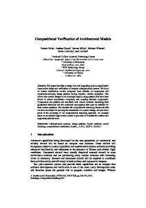
Figure 6 is the pin diagram of the analog driver of the battery charger circuit. The analog driver BATT ANA communicates with the digital part of the circuit with its interface pins. Usually in a industry standard battery charger circuit number of such pins is much more as there are some other modes of operation namely, Bad Battery Mode, USB Mode etc. and several programmable features are available. For example, the termination voltage, restart voltage level, precharge current, fullrate current etc. are programmable. Figure 7 shows pictorial representation of the mode sequence chart for BATT ANA. It has 6 states and 18 transitions, RESET being the initial state. CONST_ CURRENT
PRECHG
LDO
RESET
CONST_ VOLTAGE
MAINTY
Fig. 7. Mode Sequence Chart for the Analog part of the Battery Charger
For two states viz. CONST CURRENT and CONST VOLTAGE, assumptions and guarantees are provided in a tabular form in Table 2 along with some of the attributes of the interface pins at these states.
4
Interconnection Modeling
In the previous section we have discussed how we model the design blocks. We also need a model to capture the interconnection between the design modules. In Figure 8 three blocks are shown to be connected. To model the fact that pin a, pin b and pin c of M1, M2 and M3 are connected together we use the following three constraints.
v(a) = v(b) = v(c) i(a) + i(b) + i(c) = 0 f (a) = f (b) = f (c)
(2) (3) (4) 11
Table 2 Assume and Guarantee of CONST CURRENT and CONST VOLTAGE states GUARANTEE STATE ASSUME CONSTRAINT CONSTRAINT
ATTRIBUTE
CONST
1. 2. 3. 4. 5. 6.
i(out)=1 ¬cv ¬eoc ¬ov 3