AbstractâHighly linear 3-level unit elements are available in any fully differential circuit. This is because each unit element in such a circuit can be either ...
IEEE TRANSACTIONS ON CIRCUITS AND SYSTEMS—II: ANALOG AND DIGITAL SIGNAL PROCESSING, VOL. 47, NO. 11, NOVEMBER 2000
1177
A Study of Dynamic Element-Matching Techniques for 3-Level Unit Elements Pieter Rombouts, Member, IEEE, and Ludo Weyten, Member, IEEE
Abstract—Highly linear 3-level unit elements are available in any fully differential circuit. This is because each unit element in such a circuit can be either positively selected, negatively selected, or not selected. This paper presents a study of dynamic element techniques for such elements. It is shown how traditional dynamic element-matching techniques for 2-level unit elements such as the data directed swapper, the vector selector, and the tree structure can be adapted toward linear 3-level elements. In all these cases, the amount of hardware is reduced significantly by using 3-level elements. Also several efficient “data weighted averaging”-like implementations are presented. Then the effect of the nonlinearity of the 3-level unit element is analyzed. It is shown that this gives an additional error contribution that may limit the performance. Therefore, several efficient techniques to shape this effect as well are introduced. Index Terms—Analog-to-digital, digital-to-analog, dynamic element-matching, spectral shaping.
I. INTRODUCTION
S
IGMA–DELTA ( ) modulation is widely recognized as a proven technique to realize high- and very high-resolution A/D and D/A converters. Traditional implementations use a single-bit quantizer which is inherently linear. However, even higher performance can be obtained with a multi-bit quantizer. Among the many advantages of this, one can mention reduced filter requirements and reduced susceptibility to modulator instability, allowing a more aggressive noise shaping and reduced sensitivity to clock jitter [1]. However, such a multi-bit modulator needs a sufficiently linear and preferably low-noise multi-bit D/A converter (DAC). This has been the driving force for research in dynamic element-matching techniques [1]–[16]. These techniques allow to realize a very linear multi-bit DAC. Although the DAC usually also produces an amount of mismatch noise, this additional noise contribution can be shaped as well [1]–[15]. In [2] a thorough theoretical study of these DAC’s was already given. Also many practical techniques for dynamic element matching have already been presented. Almost all these techniques are for 2-level unit element DACs, i.e., the DAC consists of a number of elements that can be switched in two states: either selected or not. However, today most high-performance circuit implementations are fully differential. Here a very
Manuscript received February 2000; revised June 2000. This paper was recommended by Associate Editor G. Cauwenberghs. The authors are with the Electronics and Information Systems Laboratory, Ghent University, B-9000 Gent, Belgium. Publisher Item Identifier S 1057-7130(00)09925-0.
linear 3-level unit element is available [15], [17], [18]. This is because each unit element can now be either positively or negatively selected or not selected at all. Until now all the fully differential implementations of mismatch shaping DACs use only 2-level unit elements. If 3-level unit elements were used, only half the amount of unit elements would be required. This results in a simplified layout of the analog part with much less routing, switches, and associated parasitics. As will be shown in the following sections, the use of the linear 3-level unit element also results in a reduced compexity of the element-selection logic. A previous paper already addressed the problem of dynamic element matching for the fully differential 3-level element and introduced a double-index averaging technique [15]. However, the approach is not general and cannot be generalized toward higher order mismatch shaping. Also no analysis of the effect of the nonlinearity of the 3-level unit element was performed. In this paper, a study of theoretical and practical issues of dynamic element-matching techniques for 3-level unit elements is presented. It is shown how traditional dynamic element-matching techniques for 2-level elements can be adapted toward linear 3-level elements. This is done for the data-directed swapper, the tree and the vector-selector structure. Also very efficient “data weighted averaging” (DWA)-like structures are presented. Then it is shown that with these modified techniques, the main performance limiting factor is the (very small) nonlinearity of the fully differential (3-level) unit element. Several techniques to shape this error contribution are presented as well.
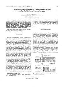
II. DYNAMIC ELEMENT MATCHING Fig. 1 represents a typical circuit implementation of the input ADC. This circuit combines the first instage of a multi-bit tegrator, the feedback DAC, and the input signal sampling. It operates in two phases. In the first phase, the input voltage is sampled on the array of unit capacitors. In the second phase, the top plates of those capacitors are switched to the operational am. Here plifier’s inputs. The bottom plates are switched to represents the element-selection value of the th capacitor. is a reference voltage. This performs an implicit D/A convermust satisfy sion. The element-selection vector the condition that
1057–7130/00$10.00 © 2000 IEEE
(1)
1178
IEEE TRANSACTIONS ON CIRCUITS AND SYSTEMS—II: ANALOG AND DIGITAL SIGNAL PROCESSING, VOL. 47, NO. 11, NOVEMBER 2000
III. A RECIPE TO ADAPT TWO-LEVEL DYNAMIC ELEMENT MATCHING TECHNIQUES TOWARDS THREE-LEVEL UNIT ELEMENTS
Fig. 1. Typical implementation of the input stage of a multi-bit converter.
61 A/D
Here, denotes the DAC input value. Now we can write the of the implicit D/A converter1 as foloutput signal lows: (2)
is the total capacitance in the array. As is common, we define the capacitor mismatch as (3) This implies that (4) Then we have because of (2) and (3)
At least three distinct classes of mismatch shaping dynamic element-matching techniques have been described. The first class consists of techniques that can be described by the vector selector2 structure of [5]. The second class is the binary tree structure [9]–[13] and the third one the data-directed swapper [1], [7]. All these structures have been described for use with 2-level unit elements where it was assumed that the DAC input . Then the code is a positive integer value with . When element-selection values can take the values 3-level unit elements are used, the element-selection values can and the DAC input code can be negative as be . well: These known mismatch shaping structures consist of a loop with a linear filter and a nonlinear selection block. When a 2-level structure must be adapted for 3-level unit elements, only the nonlinear selection block must be modified, to handle negative values as well. Now it is shown for each of these structures how this can be done. A. Vector-Selector Structure A diagram of the vector-selector structure of [5] is shown on Fig. 2(a). It consists of a “vector” control loop with a loop . This control system will minimize the norm of filter the loop filter input and therefore the element-selection vector will be set close to as well. Here, vectors are printed in bold letters. This way the DAC error term in (5) will be close to 0, too. However, the element-selection vector must still obey (1). To guarantee this, the nonlinear “vector-selector”’ block is inserted block is added to keep the input in the loop. Finally the vector of the vector-selector bounded. If the operation of the vector selector is written as an additive “noise” vector [see Fig. 2(b)], then the following result holds for the DAC error [5]:
(5) (6) . The first term is the nominal DAC output voltage The second term is an error. The basic idea of dynamic element matching is to exploit the freedom in the choice of the . Together with (4), this allows to shape the error term in (5) out of the band of interest. Traditional dynamic element-matching techniques allow only two values for the element-selection signal , e.g., or . With the highly linear 3-level unit either element that is available in a fully differential circuit [17], can take three values, [18], the element-selection signals . This has the benefit that only unit i.e., elements are required to obtain an -level DAC [15]. In the following sections, several techniques and implementations are considered to exploit this linear 3-level unit element. 1In principle, a constant factor C =C could be added to this expression for V . However, with our choice this implicit DAC has the same gain as the input signal.
Here, capital letters are used for -transforms. The sequence denotes the mismatch signal. As is common for such must be designed that its magnitude is large a structure, in the signal band. This way the DAC error will be heavily attenuated, provided the mismatch signal remains bounded. When this structure is used with 3-level unit elements, only the nonlinear vector-selector block must be modified to deal and negative element-selection with negative DAC inputs values . In [5], the 2-level vector selector was implemented by sorting its inputs . Then the elements for which the is the highest, are selected; i.e., the element-selection value is set to 1, while for the other elements, the element-selection value is set to 0. A 3-level vector selector can be very similar; still, the inputs of the vector selector are sorted. When the sign of 2Reference [5] speaks of a “vector quantizer.” However, this term has a dedicated meaning in communication theory. To avoid any misunderstanding, we shall speak of a “vector-selector”
ROMBOUTS AND WEYTEN: A STUDY OF DYNAMIC ELEMENT-MATCHING TECHNIQUES
1179
(a)
(b) Fig. 2.
(a) Actual and (b) “linearized” system diagram of “vector-selector”-based element-selection logic [5].
the DAC input is positive, the elements with the highest are selected (i.e., is set to 1) and the other elements are not selected (the element-selection value is set to 0). When is negative, the ones with the smallest are selected (i.e., their and the others to 0). element-selection value is set to It is clear that the use of the differential 3-level unit element results in a large saving of hardware in the element-selection logic: the number of filters is halved compared to the case where only 2-level unit elements are used, while the order and the complexity of each filter remains te same. The amount of hardware for the sorting operation in the vector selector is pro. Therefore, its complexity is even more portional to than halved. Also at the analog side only half the amount of capacitors, switches, and routing are required. Hereby, the associated parasitics are reduced significantly as well. B. Data-Directed Swapper and Tree Structure On Fig. 3 diagrams of the tree structured dynamic elementmatching technique of [12], [13] [Fig. 3(a)] and the data-directed swapper [Fig. 3(b)] are shown for an eight-element DAC. Both these techniques require that the number of unit elements is an integer power of two. Both systems consist of several layers , where is the of cells. The number of layers equals number of unit elements. Each cell may have several inputs, e.g., one input for the tree structure and two inputs for the data-directed swapper. However, each cell has two outputs. For each cell, the sum of all its output values must equal the sum of all its input values output
output input input input
for the tree for the data-directed swapper (7)
The difference between both outputs of each cell on layer is denoted . Then it can be shown for both the tree structure and the data-directed swapper, the mismatch error sequence can be written as [13] (8)
error
are static funcHere, denotes the time dependence. The tions of the element mismatches. The consequence of this equation is that the overall DAC error will be shaped if the sequences are shaped. To show how these structures can be adapted for the 3-level unit elements that are available in fully differential circuits, we will briefly discuss the operation with 2-level unit elements. We will do this for the tree structure of [13], but the discussion for the data-directed swapper is similar. First, we notice that the operation of each cell is determined and its input because this sets both outputs completely by output output
input input
The goal of the logic in each cell is to shape because this will shape the mismatch error [see (8)]. This is achieved by the signal processing diagram of Fig. 4. It consists of a control loop . Again, this loop will minimize the with a loop filter will be norm of the input of the loop filter and therefore set close to 0 as well. For the first-order case, this loop filter is an integrator [13], but also other filters are possible. The nonlinear “quantizer limiter” block performs the task to to a permissible integer value that is as close as possible set to the loop filter output. A permissible value is such that (7) can still be satisfied and that the outputs at the leaf end of the tree
1180
IEEE TRANSACTIONS ON CIRCUITS AND SYSTEMS—II: ANALOG AND DIGITAL SIGNAL PROCESSING, VOL. 47, NO. 11, NOVEMBER 2000
(a) Fig. 3.
(b)
Diagram of the: (a) tree structure and (b) data-directed swapper, for an 8-element DAC.
provide a legal element-selection vector. In the traditional case of 2-level unit elements where the element-selection signals can be 0 or 1, this implies the following conditions [13]: 1) both outputs are positive or 0; on the th layer, where 2) both outputs are smaller then the layers are numbered as on Fig. 3(a). When this structure is used in conjunction with 3-level unit elements, both the DAC input and the element-selection values can be negative. To achieve this, only the “quantizer limiter” blocks must be altered to allow that each cell’s input and output values can now be negative. In fact, the “quantizer limiter” is simplified because condition 1 is removed. The second condition is modified slightly: the absolute value of each output on the th layer. The rest remains the same. is smaller then This way, the final element-selection vector consists of a series ’s or ’s that satisfy (1). of 0’s and For both the data-directed swapper and the tree structure, the use of linear 3-level elements results in an important hardware reduction compared to the case where only 2-level unit elements are used. The number of cells is approximately halved for the tree and even more than halved for the data-directed swapper3 . It is also clear that the complexity of each cell is similar to the case where only 2-level elements are used. C. Computer Simulations Both for the data-directed swapper, the tree, and the vectorselector structure, the element-selection logic was simulated. First- and second-order mismatch shaping structures were investigated. As a suitable test vehicle we used a 6-bit third-order modulator ADC cascaded with a 14-bit pipeline single-loop [19]. The cascade with the pipeline was added to assure that the performance of this structure is limited by mismatch noise and not by quantization noise. Note that analog circuit imperfections in the loop filter and in the cascade stage were ignored, 3The number of cells for the data-directed swapper equals (N=2) log (N ), where N is the number of unit elements. With 3-level unit elements, the number of elements N is halved compared to conventional 2-level elements.
Fig. 4. Signal processing diagram of a cell of the tree structure of [13].
so perfect cancellation of the first-stage quantization noise was assumed. As an example, Fig. 5 shows a simulation result of the peak ratio versus the oversampling ratio for the case of no mismatch shaping, the “double index averaging” (DI) technique of [15], and first- and second-order tree structured mismatch shaping. The 32 differential (linear) 3-level unit elements were randomly mismatched with normal distribution and a %. The 9 and 15 dB/octave slopes for the first- and secondorder tree structure are clearly visible. As confirmed by [15], the DI technique does not completely achieve the characteristic 9-dB/octave slope of first-order mismatch shaping, but it performs well for moderate oversampling ratios. Without dynamic element matching, the performance is limited by low-frequency harmonics caused by the nonlinear feedback DAC. For completeness also, the simulation result of the DDWA technique that will be described in the following section is included. IV. SOME SPECIAL “DATA WEIGHTED AVERAGING” (DWA)-LIKE IMPLEMENTATIONS A. Differential DWA A very popular dynamic element-matching technique for 2-level unit elements is DWA [4]. This is because it can be implemented with only a minimum of hardware [6]. It requires only one pointer that is queued for each element that is selected
ROMBOUTS AND WEYTEN: A STUDY OF DYNAMIC ELEMENT-MATCHING TECHNIQUES
1181
Fig. 5. Simulated peak S=(N + THD) versus oversampling ratio for the first- and second-order tree structure, DI, DDWA (Section IV-A) and without dynamic element matching with linear 3-level unit elements.
Fig. 6.
Element usage for the differential DWA technique.
[4]. It can be shown that DWA can be described by a first-order vector-selector structure [5]. The DI averaging technique of [15] was a first attempt to modify the DWA technique for application with the fully differential 3-level unit element. The approach consists of setting up two DWA blocks that operate in tandem: the first DWA block is activated when the DAC input is positive, while the second takes over when the DAC input goes negative. Obviously, this approach has the disadvantage that the digital hardware is doubled. As shown in Fig. 5, it does not completely achieve the characterstic 9-dB/octave slope of first-order spectral shaping. Now we shall introduce a DWA technique suitable for the 3-level unit element. We shall denote this technique “differential DWA” (DDWA). Unlike the DI technique that requires two separate queues (one for the negative values and another one for the positive values), our approach uses only one queue. However, the queuing direction is altered each time the DAC’s input changes sign. This way only one queue pointer must value be stored. To illustrate the procedure, the element usage for the
input sequence is shown in Fig. 6 for a DAC with four 3-level elements. The asterisk indicates the location of the queue pointer. The selected elements are circled. They are depending on the sign of the DAC switched to plus or minus input . The other elements are switched to ground. For the first two input values, the operation is similar as for a single-ended DWA algorithm. However, when the input changes sign, the cycling direction is reversed. This way, the integrated error is quickly averaged out as indicated on the rightmost column of Fig. 6. Just as for the conventional DWA algorithm, it can be shown that this technique can be mapped toward a first-order vector-selector structure. Fig. 7 shows an FFT simulation result (16K FFT) of the 6-bit third-order modulator cascaded with a pipeline with the same mismatches as for the simulation of Fig. 5. The characteristic slope of first-order mismatch shaping is indicated as well. For comparison purpose, the result for the case without dynamic element matching is shown as well. It is clear that in this case, the performance is limited by low-frequency harmonics caused
1182
Fig. 7.
IEEE TRANSACTIONS ON CIRCUITS AND SYSTEMS—II: ANALOG AND DIGITAL SIGNAL PROCESSING, VOL. 47, NO. 11, NOVEMBER 2000
FFT simulation for differential DWA with linear 3-level unit elements.
Fig. 8. FFT simulation for 2-path transformed high-pass differential DWA with linear 3-level unit elements.
V. NONLINEAR 3-LEVEL UNIT ELEMENTS by the nonlinear DAC. These observations are confirmed by the simulation result of Fig. 5, where the characteristic slope of firstorder spectral shaping is demonstrated for this technique as well.
B. Bandpass Mismatch Shaping Bandpass mismatch shaping for 3-level unit element systems can be achieved by designing appropriate bandpass filters for the 3-level tree, data-directed swapper, or vector-selector structure. Here, a special case is considered that can be implemented extremely efficiently. The approach is based on a 2-path transform on a high-pass shaping technique [14]. If a high-pass mismatch transfer funccan be approximated by tion (9) Then, after a 2-path transformation, the resulting bandpass miswill be match transfer function (10) Obviously, this approach requires a doubling of the hardware compared to the high-pass shaping technique. A very efficient DWA-like high-pass shaping approach (DWAH) for 2-level unit elements was described in [14] as well. It requires only one pointer that is queued alternately left and right to obtain a mis. Similarly as in Secmatch transfer function tion IV, this technique can easily be extended toward 3-level unit elements to obtain a “differential high-pass DWA” (DDWAH) technique . Here the queue pointer is queued alternately left and right, and in addition the queue’ing direction is altered as well if the DAC input changes sign. Fig. 8 shows an FFT simulation result (128 K FFT) of a 6-bit and fourth-order bandpass modulator (two 0’s for each). The dynamic element-matching technique is the new 2-path transformed DDWAH technique. The elements had the same mismatch as for the simulations of Figs. 5 and 7. Again, the 6-dB/octave slope can be observed.
In the previous sections, we have assumed that our 3-level unit element was completely linear. An actual circuit-level implementation of this unit element may suffer from a limited amount of nonlinearity. Let us, e.g., consider the typical impleare mentation of Fig. 1. If equals 0, then both capacitors . In practice, this switched to a common-mode voltage common-mode voltage will not be perfectly in the middle of and . Due to the circuit’s nonzero common-mode gain this will give a small output signal. This means that (2) and (5) are not exact. To incorporate this effect, we should add a nonlinear term to the contribution of each unit element (11) is a nonlinear function that equals 1 for and 0 Here, represent the nonlinearity of the th 3-level otherwise. The unit element. In a good fully differential circuit design, its value can be kept very small. Since all the unit elements are nominally can be considered matched, in a first approximation all the equal. Let us call this value CM. Then (11) simplifies to
(12) The second term is an additional nonlinearity term, that we shall call the “common-mode error.” Normally, it is much smaller than the error due to the element mismatches . However, the error out of the previously described techniques push the band of interest. Therefore in a practical implementation this “common-mode error” will limit the performance. Fig. 9 shows a computer simulation result for the same structures as Fig. 5, where this effect is included in the model. CM is taken 0.01%. Comparing this with Fig. 5, we see indeed that the performance is severely degraded.
ROMBOUTS AND WEYTEN: A STUDY OF DYNAMIC ELEMENT-MATCHING TECHNIQUES
1183
Fig. 9. Simulated peak S=(N + THD) versus oversampling ratio for the first- and second-order tree structure, DI, and without dynamic element matching with nonlinear 3-level unit elements.
Fig. 10. Diagram of the element-selection logic for nonlinear 3-level unit elements with equal common-mode error.
To find a compensation for this effect, we can take inspiration of the basic idea of dynamic element matching; i.e., to shape this effect out of the band of interest. One way to do this is to try to set the number of elements that are switched to the to a constant. As indicated in common-mode voltage (12), this number is denoted . The block diagram of this approach is shown in Fig. 10. It consists of a “common-mode shaping” block and a “main mismatch shaping” block. The “common-mode shaping” block decides . This gives an extra input to the “main mismatch shaping” block. The “main mismatch shaping” block can be implemented in a simple way by adapting the vector-selector structure or the data-directed swapper, e.g., for the vector-selector structure this would give an extra condition for the vector selector. For the data-directed swapper this can be done by applying pseudothermometer encoded data to the input of elements are the swapper. This way, it is guaranteed that
switched to the common-mode voltage and the others to or . In Fig. 11(a), a possible implementation of this is shown as an example. In Fig. 11(b), a diagram of the “common-mode shaping” block is shown. It is a control loop that tries to set the number equal to a constant value. In principle, several constant values could be chosen here. However, it turns out that 1 is a good choice for this value. The control system consists of a and a “quantizer limiter.” The “quantizer loop filter limiter” performs the task to set to a permissible value as close as possible to its input, depending on the DAC input . A permissible value must be such that (1) can still be fullfilled. is the total number of unit elements, this implies the If following conditions: is odd also must be odd; 1) if is even also must be even; 2) if cannot exceed . 3) limiter” can be Based on these conditions, the “‘quantizer implemented as follows. , then all elements must be switched to mode 1: If , and therefore . plus or minus In all the other cases the, “quantizer limiter” functions according to mode 2 and 3 below. is odd, is set to 1. mode 2: if is even, is set to 0 if the loop filter output mode 3: If is smaller than 1 and to 2 else. limiter” does not have any It is clear that “the quantizer freedom in the choice of when it operates in “mode 1.” This situation is not likely to occur often, but for certain DAC inputs, it can result in instability of the loop, e.g., if the DAC input is
1184
IEEE TRANSACTIONS ON CIRCUITS AND SYSTEMS—II: ANALOG AND DIGITAL SIGNAL PROCESSING, VOL. 47, NO. 11, NOVEMBER 2000
will only be limited by the correctness of the above approximation. In reality, the may be slightly different from one another, e.g., due to mismatched charge injection from the switches. Therefore, an improved technique is presented here. Observing the operation of the “quantizer limiter” in the “common-mode shaping logic” of the previous section, we note that at most two elements are switched to the common-mode voltage. The basic idea of the new technique in this section is that always the same two elements are used for this. A simple way could be to add two extra elements for this to the normal elements. Then, the DAC error voltage can be written as (a)
error
(b) Fig. 11. Diagram of the: (a) “main mismatch shaping logic” based on a modified data-directed swapper and (b) “common-mode shaping logic.”
a constant equal to then will always be set equal to 0. This potential danger of instability can easily be eliminated by . Then restricting the DAC inputs to “mode 1” will never occur. To understand how this technique works, it is enough to note that the number is a constant a shaped sequence, provided the loop of Fig. 11(b) is stable. Since the common-mode error , the common-mode error is a constant a equals shaped sequence as well. Fig. 12 shows a simulation result of the peak ratio for our third-order modulator cascaded with pipeline test vehicle, where the new dynamic element-matching technique described in this section is used. The same 32 3-level unit elements as for the previous simulations were used. The loop of the “common-mode shaping logic” is an integrator. filter This corresponds to the simplest situation. CM is set here to 0.4%. Perhaps this is unrealistically large but it serves to demonstrate the effectiveness of the proposed approach. Both the technique with a first-order data-directed swapper [Fig. 11(a)] as the technique with a first-order vector selector were simulated. For comparison purpose also, the results without dynamic element matching and for the DI technique of [15] are added as well. Both the “‘swapper” and the “vector-selector” structure clearly realize first-order shaping. Again it can be noticed that the element-selection logic for both the data-directed swapper and the vector-selector structure is still significantly less than for the equivalent with 2-level unit elements. VI. NONLINEAR 3-LEVEL UNIT ELEMENTS REVISITED In the previous section, we have made the approximation that the nonlinearity of all the 3-level unit elements is matched. Under this approximation, it was shown that the error due to the nonlinear 3-level elements can be shaped as well. This means again that in an actual implementation, the overall performance
(13) Here, the are still defined as the relative deviation from the average value. However, the average value considered here is the average value of the first unit elements. This implies that (14) (15) The first term in (13) is the normal mismatch error. It is the same as in (5). The second term is the “extra mismatch error” due to the extra two elements and the last term is the common-mode error. The new technique tries to shape all these error contributions separately. The system diagram is represented on Fig. 13. It consists of a “common-mode shaping” block, a “common-mode difference shaping” block, “extra shaping logic,” and a “normal mismatch shaping” block. The “common-mode shaping” block is identical to the one discussed in the previous section [Fig. 11(b)]. The second block is the “common-mode difference shaping logic.” To discuss this block, we introduce the average common-mode and the common-mode difference value (16) (17) Then, the common-mode error of (13) can be rewritten as common-mode error (18) is shaped if is shaped. The error contribution Just as for the technique of the previous section, this is achieved by the “common-mode shaping” block. The remaining two terms in (18) are identical to the error of a 2-level unit element DAC. To assure this is a shaped sequence as well, any conventional 2-level dynamic element-matching technique can
ROMBOUTS AND WEYTEN: A STUDY OF DYNAMIC ELEMENT-MATCHING TECHNIQUES
1185
Fig. 12. Simulated peak S=(N + THD) versus oversampling ratio for the “data-directed swapper” and “vector-selector”-based structures with nonlinear 3-level unit elements with equal common-mode error.
Fig. 13. Diagram of the element-selection logic for 3-level unit elements with arbitrary nonlinearity.
Fig. 14.
Diagram of the “extra shaping logic.”
be used. This is achieved in the “common-mode difference and shaping” logic. It gives an intermediate result for the two element-selection values, where (either 0, 1, or
2) elements are assigned the value “0” and the other or ). elements are left unassigned (either The “extra shaping” logic serves to set these remaining element-selection values to or . This is done by the loop of Fig. 14. This loop must shape the “extra mismatch error” (second term in (13)) It consists of a loop filter and a “vector selector limiter.” This “vector selector limiter” operates as follows. 1) For the elements where is 0, the output is set to 0. elements are sorted depending on the 2) The remaining absolute value of the loop filter output. Then, for the first element of this sort of operation, the element-selection or depending on the value is assigned the value sign of its loop filter output. 3) If there is still one element with an unassigned element-selection value , then the following cases are considered, depending on the overall DAC input and the element-selection value of the other extra element: , then is assigned the value a) if ; , then is assigned the value b) if ; , then is assigned the value c) if plus or minus 1 depending on the loop filter output. Other cases cannot occur. With this operation of the “vector selector limiter,” it is guaranteed that (1) can still be satisfied. Note the difference with the conventional 2-level dynamic element-matching technique indeof [5]. Here, the loop sets each of the terms pendently to 0. This is needed because of the fact that
1186
IEEE TRANSACTIONS ON CIRCUITS AND SYSTEMS—II: ANALOG AND DIGITAL SIGNAL PROCESSING, VOL. 47, NO. 11, NOVEMBER 2000
Fig. 15. Simulated peak S=(N + THD) versus oversampling ratio for the techniques of Sections V and VI, DI and without dynamic element matching with 3-level unit elements with arbitrary nonlinearity.
[see (15)]. The loop also contains a vector selector with a sort operation, but it requires only one comparator because there are only two elements. for the normal mismatch shaping logic Finally, the input is decided as (19) When the other blocks operate as described above then this can be converted by a DAC that consists of 2-level unit elements. This means that the “normal mismatch shaping” block can consist of any conventional dynamic element-matching technique. Then the “normal mismatch” error (first term in (13) will be shaped, too. Summarizing this, we see that the entire error will be shaped. It should also be noted that the diagram of Fig. 13 in principle allows for arbitrary order noise shaping. For both the “common-mode difference shaping” block and the “normal mismatch shaping” block, any 2-level dynamic element-matching technique can be used. Also the “common-mode shaping” logic and the “extra shaping” logic can be of high order. For this technique as well, computer simulations were performed. For the “common-mode difference shaping” logic and the “normal mismatch shaping” logic, the DWA technique was used (the simplest possible implementation). Also, the “common-mode shaping” and the “extra shaping” logic were were taken randomly with an average of first order. The %. This average value and may value of 0.4% and a be much larger than in an actual implementation, but it serves to demonstrate the effectiveness of the proposed technique. The same 6-bit third-order modulator cascaded with pipeline
as in the previous sections was used. For this new technique, 34 3-level unit elements are needed. Again they are randomly mismatched % . The resulting peak ratio versus the oversampling ratio is plotted on Fig. 15. For comparison purpose also, the results for the double-index averaging technique, for the technique of Section V and for the case without dynamic element matching, are added. It is clear that the new technique achieves first-order mismatch shaping. The technique of Section V performs well for small oversampling ratios but does not maintain first-order shaping. are heavily This is expected, because in this simulation the mismatched. This confirms the excellent behavior of this new approach. VII. CONCLUSION This paper presents a study of dynamic element-matching techniques for 3-level unit elements. This is important because a highly linear 3-level unit element is readily available in any fully differential circuit. It was shown how dynamic elementmatching techniques for 2-level unit elements can be adapted to exploit 3-level unit elements, under the approximation that the 3-level unit element is completely linear. This was done for the vector-selector structure, the tree structure, and the data-directed swapper. It was shown that the use of linear 3-level element results in a significant reduction of digital and analog hardware. Also, several efficient DWA-like implementations were presented. Then the effect of nonlinearity of the 3-level unit element was investigated as well. It was shown that in a practical implementation this may limit the performance. To solve this problem,
ROMBOUTS AND WEYTEN: A STUDY OF DYNAMIC ELEMENT-MATCHING TECHNIQUES
we introduced several novel dynamic element-matching techniques. The first set of techniques is most useful when the nonlinearity contribution for the 3-level unit elements is matched. The presented approach can easily be applied to a vector-selector based technique, as well as to a data-directed swapper technique. Finally, a general mismatch shaping technique for 3-level unit elements was presented where all the 3-level unit elements can be nonlinear and arbitrary mismatched. This technique is most general, because it does not make any assumption about the 3-level unit element. The core of this method can be implemented by several nested DWA blocks, and therefore, it is very hardware-efficient as well. REFERENCES [1] R. Adams, K. Nguyen, and K. Sweetland, “A 113-dB SNR oversampled DAC with segmented noise-shaped scrambling,” IEEE J. Solid-State Circuits, vol. 33, pp. 1871–1878, Dec. 1998. [2] L. Hernandez, “A model of mismatch-shaping D/A conversion for linearized DAC architectures,” IEEE Trans. Circuits Syst. I, vol. 45, pp. 1068–1076, Oct. 1998. A/D converter incorporating a [3] B. Leung and S. Sutarja, “Multibit novel class of dynamic element matching technique,” IEEE Trans. Circuits Syst. II, vol. 39, pp. 35–51, Jan. 1992. [4] R. Baird and T. Fiez, “Linearity enhancement of multibit A/D and D/A converters using data weighted averaging,” IEEE Trans. Circuits Syst. II, vol. 42, pp. 35–51, Dec. 1995. [5] R. Schreier and B. Zhang, “Noise-shaped multi-bit D/A converter employing unit elements,” Electron. Lett., vol. 31, no. 20, pp. 1712–1713, Sept. 1995. [6] O. Nys and R. Henderson, “A 19-bit low-power multi-bit sigma-delta ADC based on data weighted averaging,” IEEE J. Solid-State Circuits, vol. 32, pp. 933–942, July 1997. [7] T. Kwan, R. Adams, and R. Libert, “A stereo multibit DAC with asynchronous master-clock interface,” IEEE J. Solid-State Circuits, vol. 31, pp. 1881–1887, Dec. 1996. [8] L. Hernandez, “Binary weighted D/A converters with mismatch-shaping,” Electron. Lett., vol. 33, no. 24, pp. 2006–2009, Mar. 1998. [9] A. Keady and C. Lyden, “Comparison of mismatch error shaping in multibit oversampled converters,” Electron. Lett., vol. 34, no. 6, pp. 506–508, Mar. 1998. [10] A. Yasuda and H. Tanimoto, “Noise shaping dynamic element matching method using tree structure,” Electron. Lett., vol. 33, no. 2, pp. 130–131, Jan. 1997. [11] A. Yasuda, H. Tanimoto, and T. Iida, “A third-order modulator using second-order noise-shaping dynamic element matching,” IEEE J. SolidState Circuits, vol. 33, pp. 1878–1886, Dec. 1998.
61
16
1187
[12] A. Keady and C. Lyden, “Tree structure for mismatch noise-shaping multibit DAC,” Electron. Lett., vol. 34, no. 17, pp. 506–508, Aug. 1997. [13] I. Galton, “Spectral shaping of circuit errors in digital-to-analog converters,” IEEE Trans. Circuits Syst. II, vol. 44, pp. 808–817, Oct. 1997. [14] T. Shui, R. Schreier, and F. Hudson, “Mismatch-shaping for a current-mode multi-bit delta-sigma DAC,” IEEE J. Solid-State Circuits, vol. 34, pp. 331–338, Mar. 1999. [15] D. Cini, C. Samori, and L. Lacaita, “Double-index averaging: A novel technique for dynamic element matching in - A/D converters,” IEEE Trans. Circuits Syst. II, vol. 46, pp. 353–358, Apr. 1999. bit converters,” [16] L. R. Carley, “A noise-shaping coder topology for IEEE J. Solid-State Circuits, vol. 24, no. 2, pp. 267–273, Apr. 1989. [17] S. Au and B. Leung, “A 1.95-V, 0.34-mW, 12-b sigma-delta modulator stabilized with local feedback loops,” IEEE J. Solid-State Circuits, vol. 32, pp. 321–328, Mar. 1997. [18] B. Ginetti, P. G. A. Jespers, and A. Vandemeulebroecke, “A CMOS 13-b cyclic A/D convertor,” IEEE J. Solid-State Circuits, vol. 27, pp. 957–964, July 1992. [19] T. Brooks, D. Robertson, D. Kelly, A. Del Muro, and S. Harston, “A cascaded sigma-delta pipeline A/D converter with 1.25 MHz signal bandwidth and 89 dB SNR,” IEEE J. Solid-State Circuits, vol. 32, pp. 1896–1906, Dec. 1997.
61
15+
Pieter Rombouts (M’97) was born in Leuven, Belgium, in 1971. He received the engineering degree in applied physics in 1994 and the Dr. degree from the Electronics and Information Systems Department in 2000, both from the University of Gent, Belgium. His technical interests are signal processing, circuits and systems theory and analog circuit design. Currently, his research focus is on data conversion.
61
16
Ludo Weyten (M’77) was born in Mortsel/Antwerpen, Belgium, in 1947. He received the Ir. and Dr. degrees from the University of Gent, Belgium, both in electrical engineering, in 1970 and 1978, respectively. From 1970 to 1972, he was with the Electronics Laboratory, University of Gent, as a Research Assistant. From 1972 to 1975, he taught at the National University of Zaire (now Congo), Lubumbashi, in a government technical co-operation project. Since 1975, he has been with the Engineering Faculty of the University of Gent, where he is currently a Professor. His teaching and research interests are in the field of electronics circuits and systems.