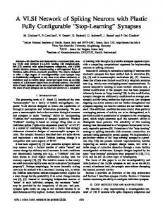
Input and output spikes are transmitted in real- time using the asynchronous Address Event Representation. Inhibitory synapse. Excitatory synapse. I&F neuron.
A VLSI network of spiking neurons with an asynchronous static random access memory Saber Moradi and Giacomo Indiveri Institute of Neuroinformatics University of Zurich and ETH Zurich Winterthurerstrasse 190, CH-8057, Zurich, Switzerland Email: [giacomo|saber]@ini.phys.ethz.ch
Abstract—In this paper we present an asynchronous VLSI neuromorphic architecture comprising an array of integrate and fire neurons and dynamic synapse circuits with programmable weights. To store synaptic weight values, we designed a novel asynchronous SRAM block, integrated it on chip and connected it to the dynamic synapse circuits, via a fast current-mode DAC. The control and data signals used for programming the weights into the SRAM, as well as the standard input and output signals, are encoded using the AER representation. The device acts as a transceiver, both receiving Address-Events in input and transmitting them as output spikes. The possibility of changing the synaptic weights via the AER protocol allows the flexibility of exploring different STDP learning algorithms in a mixed SW/HW setup. We provide experimental results measured from the chip that demonstrate the correct behavior of all the circuit blocks implemented on the chip.
Asynchronous Controller
5
978-1-4577-1470-2/11/$26.00 ©2011 IEEE
5
A E R I N P U T
SRAM 32x32 WORDS 5bits
5 5 5
NEURAL CORE
M U L T I P L E X E R
A E R O U T P U T
5
AER INPUT
I. I NTRODUCTION VLSI networks of spiking neurons offer promising solutions to problems involving realtime sensory processing and online learning of spatio-temporal patterns. A wide range of neuromorphic devices, comprising silicon neurons, synapses, and synaptic learning mechanisms has been developed in the past years (see [1] for a recent review). Many of the devices proposed comprise hardwired learning algorithms directly implemented on-chip [2]–[6], or make use of floating-gate structures which impose constraints on the learning algorithms that can be implemented [7]–[10], or do not implement biologically realistic synaptic dynamics [11], [12]. Spike-based learning mechanisms are still a subject of active investigation, and indeed a wide range of Spike-Timing Dependent Plasticity (STDP) [13], [14] learning mechanisms have been proposed in the theoretical neuroscience literature [15]–[17]. In order to explore different learning strategies in real-time VLSI neuromorphic systems it is therefore desirable to design (and hard-wire) circuits with complex synaptic dynamics, but leaving at the same time enough flexibility for changing the weight-update rules, according to the learning algorithm of interest. We present a prototype chip comprising a network of biophysically realistic silicon neurons and dynamic synapses, which incorporates also a programmable asynchronous Static Random Access Memory (SRAM) block for storing synaptic weights. Input and output spikes are transmitted in realtime using the asynchronous Address Event Representation
Bias Generator
AER INPUT
Inhibitory synapse
Excitatory synapse
Fig. 1.
Chip block diagram.
I&F neuron
(AER) [18]. Upon the arrival of an input Address-Event, the digital weight stored in the SRAM cells addressed is used to drive a Digital to Analog Converter (DAC), which outputs a current proportional to the synaptic weight value. The output of the DAC can then be used by synapse integrator circuits [19] to produce Excitatory or Inhibitory Post-Synaptic Currents (EPSC or IPSC respectively), with biologically plausible temporal dynamics. If used in their linear range, the synapse circuits can indeed be multiplexed to integrate sequences of input spikes in time. What is typically accomplished by spatial summation of currents produced by multiple instantiations of synaptic circuits, with different synaptic weights [2]–[6], is done here by using one single time-multiplexed temporal filter, and the compact asynchronous SRAM. As the AER circuits preserve the timing of the input and output spikes, this device can be used in hybrid Hardware (HW) and Software (SW) setups to explore the effect of different SW STDP learning algorithms, while executing them in real-time on the HW neural network. In this paper we describe the chip architecture and present experimental results, measured from the fabricated chip, demonstrating its correct functionality. II. T HE CHIP ARCHITECTURE The chip proposed was implemented using a standard 0.35µm CMOS process. It implements an array of hybrid
277
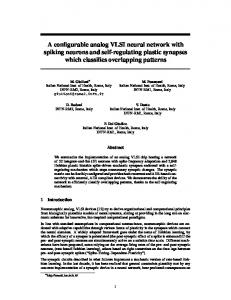
analog/digital neuron and synapse circuits interfaced to an asynchronous SRAM block [20], [21] (see Fig. 1). The overall network (neural core plus memory block) occupies an area of 1.165 mm2 , excluding pads, bias generator, and peripheral Input/Output (I/O) circuits. Input AER decoders are used to select both memory cell in the SRAM block and synapse type in the neural core. The SRAM block has 32 × 32 5 bit memory words, for storing synaptic weight values. Each bit cell in the memory was designed using a traditional 6-transistor scheme, and occupies an area of 5.25×8 µm2 . The neural core block has 32 neurons connected to 32×4 different synapse circuits (2 excitatory and 2 inhibitory synapse circuits per neuron). The bias generator block [22] is used to set all parameters required to configure the properties of synapses, neurons, and additional control circuits. Output AER encoders transmit the neuron spikes as asynchronous Address-Events. The SRAM block is digital, but fully asynchronous. The main difference with conventional SRAMs lies in the control circuitry, implemented by an asynchronous controller block which was inspired by the one originally proposed in [21]. The asynchronous controller manages the data transfer to the memory, using a standard AER link. Specifically, it enables the SRAM block to receive AER bundled-data signals in input, and to transmit dual-rail data in output. The dual-rail (1-of-2 code) representation is a type of data encoding for asynchronous communication which ensures delay-insensitive signal communication by using two wires per data bit [20]. Each SRAM word stores the value of the weight to be used by one of the four synapses belonging to the same row: when a memory word in the SRAM block is accessed, the asynchronous controller transmits the stored memory content to the corresponding synapse circuit selected by the AER input synapse decoder. The synapse circuit, implemented using the Differential Pair Integrator (DPI) proposed in [19], produces a current which is then integrated by the neuron on the corresponding row. The neuron circuits are implemented using the low-power adaptive exponential integrate-and-fire neuron described in [1]. Neurons and synapses have global parameters (i.e., all neurons have the same leak conductance, the same refractory period, etc.) Having four sets of synapses per neuron with independent parameters allows us to implement both excitatory and inhibitory synapses with two possible time constants each, providing the chip with 32×4 virtual synapses per neuron (4096 synapses in total). Figure 2 shows how the 5 bit word from the memory block is used to set the synaptic weight. The bits from the selected word are routed to the synapse and control the switches that choose the desired combination of I0 − I4 for setting Iw . As for the other parameters in the system, the five parallel current sources (I0 − I4 ) can be programmed by using the on-chip bias-generator, with currents that range from pico-Amperes to micro-Amperes. Using this scheme, classical DAC design issues (e.g. for settling times, speed, and precision) are avoided because the precise current values are set by constant global biases, and the digital data is only used for activating digital
Vdd
Vτ
Vdd
Csyn
Iτ
Vdd
Vdd
Vthr
Isyn
Iw
Vw4 b4
Iw4
Iw3
Iw2
Iw1
Vw3
Vw2
Vw1
Vw0
b3
b2
b1
Iw0
b0
Fig. 2. Current-mode DAC and excitatory synaptic dynamics DPI circuit. The DPI circuit (top yellow block) implements the synaptic response temporal dynamics, while the current-mode DAC (bottom green block), determines the amplitude of the synaptic weight current Iw .
switches. The Iw determines the maximum Isyn current produced by the DPI, which corresponds to the synapse Excitatory Post Synaptic Current (EPSC) [19]. The linear properties of the DPI circuit allow to model the effect of spatial integration of N synapses (potentially with N different weights) by temporal superposition of the EPSCs produced by subsequent AddressEvents sent to N different memory words and to the same DPI circuit. With the architecture scheme proposed, it is sufficient to use just one synapse circuit with 5 global parameters and N memory cells, rather than N instantiations of the same synapse circuit, and N global parameters. An additional source of flexibility and re-configurability is provided by a “dendritic multiplexer” circuit, placed between the synapses and the neurons (see Fig. 1) that allows to route the currents produced on each row of synapses to selected subsets of neurons. In its default configuration all the synapse circuits of each row are connected to the neurons on their corresponding row with a one-to-one mapping, thus providing 32 output neurons each with 32×4 input synapses. By using this multiplexer, synapses can be disconnected from the neurons belonging to the same row, and merged together with synapses belonging to different rows, to integrate all their output currents onto a different set of neurons. This is effectively allocating more synapses per neuron, at the cost of a reduced set of usable output neurons. In the extreme case, all rows are shorted together and connected to only one neuron circuit, thus providing one single output neuron, but with 32×32×4 inputs. This multiplexing scheme is particularly useful for applications that need to process signals with large input dimensions (e.g. images). III. E XPERIMENTAL RESULTS In this section we present preliminary test results from the fabricated device. To verify the functionality of the chip, we first programmed the SRAM cells with different digital
278
40
5 ChipReq /PixAck ChipAck
4
Spatial summation (SW) Temporal superposition (SW) Temporal supeposition (HW)
35 30
20
25
2
Isyn (nA)
AER input signals (V)
3
1
15 20
10 5
15
0 10
0
0
20
40
60
5
−1 0
−2
0
50
100 Time (ns)
150
0
200
Fig. 3. AER input signal timings: upon receiving an input chip request signal (ChipReq) the asynchronous, pipe-lined AER input circuits produce an output chip acknowledge signal (ChipAck ). Validity-check circuits in the asynchronous controller block then generate a pixel acknowledge signal (see /PixAck ) used to terminate the handshaking cycle.
words; then we measured the synapse EPSCs (Isyn of Fig. 2) and verified that the synaptic weights are properly encoded by the SRAM content; subsequently, we verified that the neuron circuits produce output spike trains in response to synaptic currents, and that the AER output circuits transmit the corresponding events accordingly. Figure 3 shows the input AER handshaking signals for a sequence of input spikes and verifies correct implementation of four-phase handshake protocol. The asynchronous digital circuits used to manage the input bundled data representation produce a ChipAck acknowledge signal in response to input ChipReq request signals. In addition, new on-chip asynchronous circuits produce a /PixAck “data valid” signal from the dual-rail output of the SRAM block, to activate the DACs that set the weighted synaptic current, and to terminate the input handshaking cycle. A useful performance metric to measure in these types of systems is the maximum number of events per second that can be consumed: as demonstrated by the ChipReq period in Fig. 3, the chip can receive approximately 5.8 M events/s. This is however due to the explicit delays programmed in the AER setup currently used. In principle the ChipReq signal could be de-asserted as soon as the ChipAck signal reaches 3.3V. In this case the maximum input rate could easily reach 10 M events/s. The measurements of the analog synaptic currents are shown in Fig. 4. For these measurements we biased all synapses to produce EPSCs with biologically realistic time-constants, of the order of tens of milliseconds, and stimulated them using different synaptic weights. The synaptic currents were measured by reading a local copy of the relevant Isyn current off-chip, and by using an off-chip current to voltage converter. We were able to verify the expected linear behavior of the DPI circuit by comparing spatial to temporal superposition effects. The HW temporal superposition trace of Fig. 4 shows the Isyn current measured from three “virtual” synapses multiplexed in time. The measurement was done by sending three subsequent
20
40 Time (ms)
60
80
100
Fig. 4. Synaptic circuit response to three different weighted inputs measured from different virtual and physical synapses (see text for details). The figure inset shows the measured individual responses for the three different weight settings.
address-events to three different memory cells (with different weight values stored) connected to the same physical DPI circuit. For comparison, we also computed the temporal and spatial superposition of the three measured EPSCs in SW. For the SW spatial superposition computation, we measured the EPSC of three distinct DPI circuits on different rows, using the same weight values used for the virtual synapses. For the SW temporal superposition computation we measured the EPSC of the same DPI circuit for three different times, each time with one of the three different weight values used before. We recorded the individual responses and summed the three traces in SW. The inset of Fig. 4 shows the individual EPSC measurements of all real and virtual synapse responses. The digital synaptic weight bits stored in the memory cells of the first row are: 00111, 01010 and 01101 respectively, while the DAC biases Vw0−4 of the synapse were biased at 1.3V, 1.5V, 1.7V, 1.9V and 2.1V respectively. The fact that the temporal superposition done in HW is equivalent to the spatial (and temporal) summation done in SW demonstrates that the DPI circuit behaves as a linear filter. The minor differences present in the data are most likely due to device mismatch effects present in the different synapse circuits used. In addition to saving precious silicon real-estate, the strategy of using a single multiplexed DPI to implement multiple (virtual) synapses on each neuron has also the benefit of eliminating the problem of device mismatch effects. In a final experiment we tested the functionality of the whole signal pathway, from the input AER circuits to the output AER ones. We initialized synaptic weights with two different values: a low value for the top half of the array, and a high value for the bottom half. We then stimulated the first excitatory synapse of each neuron in the array with a regular spike train at 200 Hz for two seconds. The raster plot shown in Fig. 5 demonstrates the correct functionality of the overall chip, showing how the events in input produce events in output with the expected firing rates. We used only two synaptic weight values to point out how device mismatch effects are very small, even when
279
Neuron
31
15
0 0
100 Time (ms)
200
0
200 Frequency (Hz)
Fig. 5. Left: raster plot of the silicon neuron spikes, in response to regular input spike trains of 200 Hz, sent to synapses with two different synaptic weight settings. Right: histogram of the neuron mean frequencies.
looking at the full input-output signal pathway (see histogram of Fig. 5). IV. C ONCLUSION We proposed a novel device comprising both a neuromorphic “neural core”, with biophysically realistic analog synapse and neuron circuits, as well as a fully asynchronous digital memory block. We presented experimental results, demonstrating the proper functionality of all the major circuit blocks the chip: the data of Fig. 3 and Fig. 4 demonstrate that input events are successfully transmitted through the input AER stages onto the SRAM block, that the SRAM provides in output the expected bits (previously programmed into the memory), that the synapse converts the stored digital word into a properly weighted synaptic current, and that the synaptic dynamics block has the expected linear filtering properties. The data of Fig. 5 shows that the synaptic currents get properly integrated by the spiking neurons and that the spikes get properly converted into AER events and transmitted by the output AER stages. We now plan to apply the chip proposed for testing different STDP learning strategies in the context of real-time neuromorphic sensory-motor systems. ACKNOWLEDGMENT This work was supported by the European Community’s Seventh Framework Programme: grant #231467 – eMorph. The authors would like to thank the whole NCS group (http:// ncs.ethz.ch/) for support and contributions to the development of the AER experimental setup. R EFERENCES [1] G. Indiveri, B. Linares-Barranco, T. Hamilton, A. van Schaik, R. Etienne-Cummings, T. Delbruck, S.-C. Liu, P. Dudek, P. H¨afliger, S. Renaud, J. Schemmel, G. Cauwenberghs, J. Arthur, K. Hynna, F. Folowosele, S. Saighi, T. Serrano-Gotarredona, J. Wijekoon, Y. Wang, and K. Boahen, “Neuromorphic silicon neuron circuits,” Frontiers in Neuroscience, vol. 5, no. 0, 2011.
[2] S. Mitra, S. Fusi, and G. Indiveri, “Real-time classification of complex patterns using spike-based learning in neuromorphic VLSI,” IEEE Transactions on Biomedical Circuits and Systems, vol. 3, no. 1, pp. 32–42, Feb. 2009. [3] M. Giulioni, P. Camilleri, V. Dante, D. Badoni, G. Indiveri, J. Braun, and P. Del Giudice, “A VLSI network of spiking neurons with plastic fully configurable “stop-learning” synapses,” in International Conference on Electronics, Circuits, and Systems, ICECS 2008. IEEE, 2008, pp. 678–681. [4] J. Schemmel, D. Br¨uderle, K. Meier, and B. Ostendorf, “Modeling synaptic plasticity within networks of highly accelerated I&F neurons,” in International Symposium on Circuits and Systems, ISCAS 2007. IEEE, 2007, pp. 3367–3370. [5] A. B. i Petit and A. Murray, “Synchrony detection and amplification by silicon neurons with STDP synapses,” IEEE Transactions on Neural Networks, vol. 15, no. 5, pp. 1296–1304, September 2004. [6] E. Chicca, D. Badoni, V. Dante, M. D’Andreagiovanni, G. Salina, S. Fusi, and P. Del Giudice, “A VLSI recurrent network of integrate–and–fire neurons connected by plastic synapses with long term memory,” IEEE Transactions on Neural Networks, vol. 14, no. 5, pp. 1297–1307, September 2003. [7] F. Tenore, J. Vogelstein, R. Etienne-Cummings, G. Cauwenberghs, and P. Hasler, “A floating-gate programmable array of silicon neurons for central pattern generating networks,” in International Symposium on Circuits and Systems, ISCAS 2006. IEEE, 2006. [8] C. Gordon, E. Farquhar, and P. Hasler, “A family of floating-gate adapting synapses based upon transistor channel models,” in International Symposium on Circuits and Systems, ISCAS 2004, vol. 1. IEEE, May 2004, pp. 317–20. [9] P. H¨afliger and C. Rasche, “Floating gate analog memory for parameter and variable storage in a learning silicon neuron,” in International Symposium on Circuits and Systems, ISCAS’99. Orlando: IEEE, 1999. [10] C. Diorio, P. Hasler, B. Minch, and C. Mead, “A floating-gate MOS learning array with locally computed weight updates,” IEEE Transactions on Electron Devices, vol. 44, no. 12, pp. 2281–2289, December 1997. [11] F. Tenore, R. Etienne-Cummings, and M. Lewis, “A programmable array of silicon neurons for the control of legged locomotion,” in International Symposium on Circuits and Systems, ISCAS 2004. IEEE, 2004, pp. 349–352. [12] U. Mallik, R. Vogelstein, E. Culurciello, R. Etienne-Cummings, and G. Cauwenberghs, “A real-time spike-domain sensory information processing system,” in International Symposium on Circuits and Systems, ISCAS 2005, vol. 3. IEEE, 2005, pp. 1919–1922. [13] G.-Q. Bi and M.-M. Poo, “Synaptic modifications in cultured hippocampal neurons: Dependence on spike timing, synaptic strength, and postsynaptic cell type,” Jour. of Neuroscience, vol. 18, no. 24, pp. 10 464–10 472, 1998. [14] L. Abbott and S. Nelson, “Synaptic plasticity: taming the beast,” Nature Neuroscience, vol. 3, pp. 1178–1183, November 2000. [15] C. Clopath, L. B¨using, E. Vasilaki, and W. Gerstner, “Connectivity reflects coding: a model of voltage-based STDP with homeostasis,” Nature Neuroscience, vol. 13, no. 3, pp. 344–352, 2010. [16] T. Masquelier, R. Guyonneau, and S. J. Thorpe, “Competitive stdp-based spike pattern learning,” Neural Computation, vol. 21, pp. 1259–1276, 2009. [17] M. Graupner and N. Brunel, “Stdp in a bistable synapse model based on CaMKII and associated signaling pathways,” PLOS Computational Biology, vol. 3, no. 11, pp. 2299–2323, 2007. [18] J. Lazzaro, J. Wawrzynek, M. Mahowald, M. Sivilotti, and D. Gillespie, “Silicon auditory processors as computer peripherals,” IEEE Transactions on Neural Networks, vol. 4, pp. 523–528, 1993. [19] C. Bartolozzi and G. Indiveri, “Synaptic dynamics in analog VLSI,” Neural Computation, vol. 19, no. 10, pp. 2581–2603, Oct 2007. [20] J. Lin, P. Merolla, J. Arthur, and K. Boahen, “Programmable connections in neuromorphic grids,” in 49th Midwest Symposium on Circuits and Systems. IEEE, 2006, pp. 80–84. [21] V. Ekanayake and R. Manohar, “Asynchronous dram design and synthesis,” in Ninth International Symposium on Asynchronous Circuits and Systems. Vancouver, BC: IEEE, May 2003, pp. 174–183. [22] T. Delbruck and P. Lichtsteiner, “Fully programmable bias current generator with 24 bit resolution per bias,” in International Symposium on Circuits and Systems, (ISCAS 2006). IEEE, 2006.
280