AcENoCs: A Configurable HW/SW Platform for FPGA Accelerated NoC Emulation Swapnil Lotlikar, Vinayak Pai and Paul V. Gratz Department of Electrical and Computer Engineering, Texas A&M University camsin
[email protected] http://cegroup.ece.tamu.edu/camsin/acenocs/ Abstract— The heterogeneous nature of the modern day applications has resulted in widespread use of Multicore SoC architectures. The emerging Network-On-Chip (NoC) interconnect architecture provides an energy-efficient and scalable communication solution for multiple cores, serving as a powerful replacement for traditional bus architectures. The key to the successful realization of such architectures is a flexible, fast and robust emulation platform. This paper presents the design, implementation and evaluation of AcENoCs, a flexible and cycle-accurate FPGA emulation platform for validating synchronous and GALS-based NoC architectures. The emulation platform is built around a HWSW framework consisting of reconfigurable network components, traffic generators and ejectors, statistics collection and analysis modules. We also address the unique features of our platform in terms of reconfigurability and co-design of the hardware and software components, and assess the performance improvements and tradeoffs over existing FPGA emulators and software simulators. Our experimental analysis indicate speedup improvements in the order of 10000-12000X over HDL simulators and 14-47X over software simulators, without sacrificing cycle accuracy.
I. I NTRODUCTION With the rapid advancements in VLSI technology, the number of components integrated on a single chip has multiplied significantly. In order to meet processing demands, current SoC designs incorporate a large number and a wide variety of IP cores on a single chip. Traditionally, buses have been used as a medium for efficient inter-core communication. Buses, however, have scalability issues which limit their usage to interconnecting small number of cores. A new design paradigm, Network-on-Chip (NoC), proposed by Dally and Towles, serves as an effective replacement for buses in a system with large number of processing cores, offering high communication bandwidth with low latency [1]. Due to increase in inter-module communication requirements and demand for reduced time-to-market, validation of communication infrastructure plays a major role in chip design. A fast exploration of the vast NoC design space is vital to arrive at an optimal interconnect configuration for meeting the demands of a particular application. Typically, this is accomplished using software or HDL simulators and consumes a significant fraction of the overall chip design time. Fast, cycle-accurate FPGA emulators have been used as an alternative to software simulators as they reduce the validation time without compromising accuracy [2]. FPGA emulators permit the user to exploit the parallel nature of hardware and simulate the HDL at actual hardware speeds, thereby detecting design and architectural problems early and reducing the number of chip respins. Several previously proposed FPGA based NoC emulation schemes focus on achieving high emulation performance at the cost of reduced emulated network sizes [2, 3], while * Mr. Lotlikar and Mr. Pai contributed equally to this paper; their names are placed alphabetically in the author list.
others aim at emulating larger dimension networks sacrificing performance [4, 5]. There is a great demand for emulation schemes which strike an optimum balance between emulation performance and emulated network dimensions. The main contribution of this paper is the co-design of a fast, cycleaccurate and flexible FPGA-accelerated HW/SW NoC emulation platform, AcENoCs (Accelerated Emulation platform for NoCs), for performing quick exploration and validation of NoC design features. This paper also details the various design optimizations and tradeoffs between network size and performance in AcENoCs’ HW/SW co-design. AcENoCs is capable of emulating synchronous as well as Globally Asynchronous Locally Synchronous (GALS) based NoC architectures [6]. The NoC is modeled using the FPGA’s hardware resources, and hence efficiently exploits the parallelism in hardware as opposed to sequential software simulators. Given limited FPGA resources, AcENoCs can support larger dimension NoCs as compared to other emulators and can operate at speeds greater than software simulators. The traffic models and statistics analysis are implemented in software, utilizing a soft IP processor, leveraging the greater state space resources available to software and freeing additional FPGA resources. AcENoCs’ hardware framework supports exploration of a wide range of router features and network configurations, while the software framework allows for easy reconfiguration of emulation parameters and defines a plug-and-play interface for integrating with different router architectures and NoC topologies. AcENoCs follows a well-defined emulation flow for synchronizing various HW/SW events during emulation process. AcENoCs’ high emulation performance and utility can be attributed to HW/SW codesign optimizations based on hardware resource evaluation and software profiling results. The rest of the paper is organized as follows. Section II describes related work. Section III and IV describes AcENoCs’ emulation framework and HW/SW interaction. Section V presents AcENoCs’ performance evaluation followed by conclusions in Section VI. II. R ELATED W ORK Several simulation methods and tools have been developed to speed up the verification of on-chip communication architectures. These methods can be broadly classified under two categories – software simulators and FPGA based emulators. A. Software Simulators Researchers have proposed several SystemC based environments to perform NoC modeling and simulation at the system level early in design cycle [7, 8, 9]. These system level simulators compromise cycle accuracy for simulation speed. Several cycle accurate NoC simulators have also been developed [10, 11, 12]. The major drawback with these software simulators is their sequential nature of execution. Their simulation speed degrades with a move towards lower levels
of abstraction and higher network sizes, making simulation time prohibitive for real application traffic. B. FPGA Based Emulators Genko et al. propose an emulation platform using Xilinx Virtex-II Pro FPGA (XUPV2P) with an embedded PowerPC processor, emulating a network comprised of 6 routers [2]. The hardware platform is comprised of traffic models and the emulation network, while the software handles platform configuration and controls entire emulation process. Source queues are modeled in hardware. Another emulation scheme, NoCOP, for a 4x4 mesh network is proposed by Liu et al. [3]. NoCOP’s hardware framework proposed is similar to Genko’s scheme. An external Instruction Set Simulator is used instead of an embedded processor to control and configure the emulation system. Krasteva et al. propose an emulation framework based on partial reconfiguration of FPGAs that accelerates the emulation process by eliminating the need for hardware resynthesis in case of network reconfiguration [13]. However, due to high area overhead, this scheme emulates a smaller 4-node network on Xilinx Virtex-II FPGA. DART FPGA emulation platform aims at emulating different NoC topologies without the need for hardware resynthesis. It implements a 9-node network on a XUPV2P FPGA at the cost of performance, by serializing the switching inside the router [5]. The emulation framework is similar to that of Genko’s. DART’s router uses minimal FPGA resources, replacing area consuming allocation arbiters and crossbar with simple arbiters and multiplexers, thereby limiting its throughput to a single flit per FPGA cycle. Another emulation platform, NoCem, employs real processing cores to generate traffic and emulates a 3x3 NoC on XUPV2P FPGA using lightweight, non-pipelined routers without virtual channels [14]. For emulating large scale NoCs, multi-FPGA emulation schemes have been proposed [15]. In such schemes, off-chip delays cause performance bottleneck and size of NoCs is limited by available FPGA I/O pins and additional overhead for inter-FPGA communication adapters. Another scheme to emulate large homogeneous and heterogeneous NoCs is presented by Wolkotte et al.[4]. Here, a large NoC is simulated by sequentially evaluating each router on a single router model instantiated in an FPGA. The state associated with each simulated router and its links is stored in memory and retrieved when necessary. Non-exploitation of true parallel nature of hardware along with off-chip delays limit the speedup achieved to only 80-300X compared to a SystemC simulator. In this paper, we present an HW/SW emulation framework, AcENoCs, which overcomes the shortcomings of both the software simulators and previous FPGA emulation platforms in terms of speed, cycle accuracy and FPGA resource consumption. AcENoCs’ router is a single-stage, low latency router capable of routing multiple flits in a single FPGA cycle. In our framework, the traffic generators (TGs), traffic receptors (TRs), analysis modules and source queues are all implemented in software, thereby freeing additional FPGA resources for the implementation of a larger network on hardware. In addition to emulation of synchronous NoCs, emulation of GALS based NoCs is a unique feature supported by AcENoCs as compared to previous FPGA emulation schemes. III. N O C E MULATION F RAMEWORK AcENoCs is a cycle accurate emulator instantiated on Xilinx XUPV5 FPGA board, containing a Virtex-5 (VLX110T) FPGA. AcENoCs is centered around HW/SW framework with the FPGA’s hardware resources constituting the hardware
To RS232 and Display BRAM Memory
UART Controller P R O C E S S O R
SOFTWARE FRAMEWORK
Traffic Generators (TGs)
HARDWARE FRAMEWORK
R
R
R
R
Source Queues L O C A L
Emulation Clock Gen
Traffic Receptors (TRs)
B U S
Emulation Network Hardware Register Bank
Virtex-5 FPGA
SysACE CF Controller
From Compact Flash (Read Trace Files)
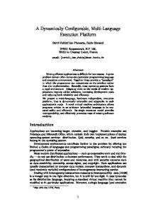
Fig. 1: AcENoCs Emulation Framework framework and the MicroBlaze soft core processor and the associated peripherals constituting the software framework as shown in Figure 1. The hardware and the software framework interact with each other using Processor Local Bus (PLB). A. Hardware Framework The hardware framework of the AcENoCs emulation platform comprises of the interconnection network to be emulated. The NoC is constructed using a custom built hardware library of routers and links. The routers are interconnected using links according to the specified topology. Routers can operate synchronously on a common network clock or each router can operate on an independent clock. A routing scheme decides how a packet traverses through the network to reach its destination. A packet is sub-divided into smaller units called “flits”. A flow control scheme decides the allocation of network resources to a flit. Virtual channel based flow control instantiates several buffers per physical channel, thereby increasing network throughput and avoiding deadlocks. 1) NoC Router: As Figure 2 illustrates, the AcENoCs’ NoC router is a standard 5-port single-stage pipelined router comprising of an input unit, routing unit, virtual channel allocation unit, switch allocation unit, crossbar and an output unit. The total number of ports on the router can be configured. The local port of the router is connected to the TG/TRs in the emulation platform. A brief explanation of these components is given here, more details can be found in [16]. VC ALLOCATION SWITCH ALLOCATION
INPUT UNIT
OUTPUT UNIT CROSSBAR SWITCH
INPUT DATA INPUT UNIT
R O VC0 VCn
NRC
OUTPUT DATA OUTPUT UNIT
CREDIT CNTR n VC n STATE DELAY REGS
Fig. 2: Router Architecture Input Unit: This unit is instantiated per input port. It receives flits from the neighboring routers and buffers them in the virtual channel (VC) fifos (VC0-VCn). The number of VCs and the depth of each VC fifo is configurable. Each input 2
unit also consists of a next hop routing computation (NRC) unit, implementing the look ahead routing technique [17]. This scheme enables the route computation to be done in parallel with switch and VC allocation. Currently, AcENoCs supports deadlock-free, XY dimension order routing (XYDOR). Alternate routing algorithms can be easily implemented by modifying the functionality of NRC. VC Allocation Unit: This unit allocates an output VC to a packet from amongst available VCs at the output port. The VC allocator is implemented as a two level allocator [18]. The arbiter implements both round-robin and fixed priority. Switch Allocation Unit: This unit controls the access to the crossbar unit. Like the VC allocator, this also has two levels of arbitration. The switch allocation is done speculatively with VC allocation, thus reducing the router pipeline latency [19]. The arbiter implements both round-robin and fixed priority. Crossbar: The crossbar provides data path between input and output ports and is designed using two levels of multiplexers. The access to the crossbar is controlled by the switch allocation unit. Output Unit: This unit maintains the status of output VC (free/active) and keeps track of credits available in the downstream router’s VC fifo using credit based flow control [16]. Programmable Delay Unit: This unit can be configured to emulate a variable depth pipeline or link delay. It contains series of programmable registers that delay the valid output data from appearing on the link. 2) Design Optimizations and Analysis: Typical NoC routers are connected together by links of a given width. These links carry data flits between routers and their width directly affects the number of flits required to transmit a complete packet. In AcENoCs, although the actual link width of the instantiated routers is 32 bits, the minimum required to carry route information in head flit, different link widths can be easily emulated by changing the number of flits per packet. Two memory options were available for implementing the VC fifos: dual port Block RAM (BRAM) or dual port Distributed RAM which utilizes FPGA’s LUTs. BRAM is available only in fixed block sizes and is typically used for realizing larger memories, while Distributed RAM is used for implementing smaller sized memories. Since the memory requirements for VC fifos is small, Distributed RAM was used. For many topologies such as 2D mesh, there exists unused router ports on the periphery of the network. In order to fit a maximum dimension network on FPGA, 3-port and 4-port routers were used along the network boundaries.
generate various flit fields including flit type, packet destination address, source router’s output port for flit forwarding, source router’s local port input VC identifier and packet id for each packet. Each TG also plays an active role in packet latency bookkeeping by storing the network cycle, when a packet was injected into its source queue, in a separate data structure. This structure can be indexed using the injected packet’s source id and packet id fields. There are two broad classes of traffic supported by the TGs: Synthetic workloads and Realistic workloads. Synthetic Traffic Generator: AcENoCs Synthetic TGs are implemented on a single MicroBlaze processor running at 125MHz. It supports common synthetic workloads including uniform random, bit complement, bit reversal, matrix transpose, bit shuffle, bit rotation and hotspot [16]. Packet generation is governed by a uniform random injection process. The probability of each node generating a packet in an emulation cycle depends on the user specified flit injection rate. This process involves generation of a uniform random number for each TG in every emulation cycle. AcENoCs uses an XOR-shift algorithm for generating uniform random numbers [20]. This algorithm was chosen due to its ability to generate highly accurate uniform random numbers within a specified range and most importantly, its consumption of much fewer processor cycles per random number than other techniques examined such as glibc’s rand() function. Trace-based Traffic Generator: AcENoCs supports network evaluation using real application traces. The processor reads and decodes each trace line from a flash card to generate a packet. Each trace line contains source and destination node coordinates of the packet along with the network injection cycle. Reading from flash card incurs huge processor latencies, resulting in degradation of the emulator performance. To counter this, AcENoCs implements a dual-processor environment (MicroBlaze1/MB1 and MicroBlaze2/MB2), with software on MB1 implementing a trace based TG and software on MB2 dedicated for reading the traces from flash card. The MB2 prefetches and passes the trace data to MB1 through a Shared BRAM fifo (SHBRAM). Hence, the trace read operation in MB2 is overlapped with the actual execution of the traces in MB1 and the trace execution can be directly started without any delay due to trace file I/O operations. Owing to the prefetching mechanism, AcENoCs is able to achieve significant speedups for emulating realistic workloads, as compared to software simulators. This environment synthesizes at a maximum frequency of 100MHz. 2) Source Queues/FIFOs: The source queues associated with each router provide temporary storage for packets prior to network injection. Each source queue is implemented in software and operates in a FIFO fashion. They are dynamically allocated at runtime during the emulation process. The width of each queue location is equivalent to the emulated flit width. The total number of outstanding flits across all source queues is calculated at compile time depending upon the remaining software memory after the software program is loaded into memory. In every emulation cycle, flits are read from nonempty queues and transmitted to the corresponding router through input data and data valid registers. By opting for software based source queues, premature packet throttling in case of non-uniform traffic is avoided. 3) Traffic Receptor (TR): Each router is also associated with a TR, which decodes the information in packets received at the destination router and validates its destination. TRs also calculate the latency for each received packet. At the end of
B. Software Framework Figure 1 shows AcENoCs’ software framework consisting of Traffic Generators (TGs), Source Queues, Traffic Receptors (TRs) and dynamically controlled Emulation Clock Generator. The software framework is implemented on embedded MicroBlaze processor and controls the emulation process via emulation configuration file. MicroBlaze is a 5-stage pipelined processor and operates at a max. frequency of 125MHz. An on-chip BRAM stores the software running on the processor. Alternately, external DDR2 RAM can also be used, but at the cost of reduced emulation performance due to increased access latencies. The emulation clock driving the network components is dynamically generated by the processor. 1) Traffic Generators (TG): Each router is associated with a software-based TG, which generates packets and feeds them to its source queue. TGs are responsible for building the flits and inserting them into its source queue. For building flits, TGs 3
the emulation, the average latency per packet is computed. Passing the received packet from the router to its associated TR is coordinated through output data and status registers. 4) Emulation Clock Generation: The emulation clock driving the network is dynamically generated by the MicroBlaze processor (MB1 for trace based TG). Each emulation cycle consists of multiple processor cycles and contains an ordered sequence of hardware and software events. Generating the emulation clock in software helps in achieving synchronization between the software and hardware events occurring every emulation cycle. The dynamic control of the emulation clock is based on per emulation cycle SW operation latency. The emulation clock is allowed to proceed to the next emulation cycle only when the SW completes its traffic generation and reception for that cycle. The dynamic approach is more efficient than statically clocking the FPGA based on worst case SW latency, since the FPGA hardware can now operate on a much faster clock. Since the clock rate depends on software latency per emulation cycle, it decreases with increasing network size. The clock is relayed to hardware through clock register. 5) Design Optimizations and Analysis: There are two possible implementations of MicroBlaze: the area optimized 3stage pipeline and the frequency optimized 5-stage pipelined version. The 3-stage design synthesizes at 100MHz as compared to 125MHz in the 5-stage version. The traffic generation and reception process involves multiple calls to various functions, which maps to branches in the assembled code, incurring 2 cycle penalty (1 cycle penalty with branch delay slot) for both versions of MicroBlaze. This implies lower branch resolution time for the 5-stage pipeline. This combined with the higher operating frequency of 5-stage pipeline gives higher performance as compared to the 3-stage pipeline. To reduce the performance impact due to branch penalties, optimizations like loop unrolling, function inlining and reducing function calls were carried out on the software to reduce the branches. To improve emulator performance, we also choose to instantiate a floating point unit (FPU) and a hardware barrel shifter as add-ons to the MicroBlaze. Hardware implementation of TGs/TRs incurs additional overhead in terms of FPGA logic resources required to implement them. With increasing network sizes, the amount of hardware resources utilized for TGs and TRs increases proportionally, leading to inefficient use of the FPGA hardware resources. Implementing the TGs and TRs in software allows efficient use of the FPGA resources by making room for additional routers, thereby realizing a larger network. In earlier FPGA emulation schemes [2, 3, 5], the source queues were implemented in hardware, and their depths allocated statically at compile time. This forces the emulator to prematurely throttle the packet generation under nonuniform traffic. Throttling of packets has implications on the packet injection rate since the rate drops below its specified value. This might result in non accurate modeling of network congestion conditions. AcENoCs overcomes this limitation by dynamically allocating source queues. AcENoCs is able to sustain transitory injection rates higher than the network saturation injection rate for a longer time, thereby providing more accurate packet latency and network throughput analysis. Packet throttling is initiated when source queues overflow for injection rates higher than the network saturation rate.
nected to the Processor Local Bus (PLB). The registers can be classified as clock register, input data and data valid registers, output data registers, input status and output status registers. The clock register provides software controlled clock to the network, input data and data valid registers are used to inject flits into the router’s local port. The output data registers capture the flits ejected from the network. The input status registers contain VC fifo full status, the output status registers indicate the flit arrival at the destination router. D. Emulation of GALS NoCs With the emergence of SoC design methodologies and a need to alleviate chip power consumption, researchers are adapting GALS based design styles. AcENoCs is capable of emulating synchronous as well as GALS based NoCs on a common hardware platform, thereby enhancing the versatility offered by the emulation platform. For GALS NoCs, where the NoC is divided into partitions and each partition operates on an independent clock, the number and distribution of the clock domains across network nodes can be configured through a user specified emulation configuration file. The software generates and distributes network clocks to the respective routers via clock registers. The clock domains are mesochronous, generated by offsetting their rising edges. The asynchronous input VC FIFOs at each node act as data synchronization elements across clock boundaries. The FIFO’s write interface is sourcesynchronous and operates on the upstream router’s clock, while the read interface is synchronous with the local router’s clock. Packet latency is greater due to the synchronization overhead across clock boundaries. By supporting emulation of GALS NoCs, AcENoCs serves as an ideal platform for validating GALS NoC architectures such as ABC [21]. IV. N O C E MULATION HW/SW F LOW We realized the AcENoCs emulation framework using the Xilinx Embedded Development Kit (EDK). In this section, we present a detailed description of AcENOCs’ complete hardware software emulation flow. A. Configuration The user configures AcENoCs via two configuration files, emulation configuration file for SW framework and network configuration file for HW framework. The emulation process is controlled by parameters in the emulation configuration file such as packets to be injected, flit injection rate, traffic pattern, packet sizes, distribution of clock domains, etc. The network configuration file enables the user to configure network dimensions and topology, router data width, arbitration scheme, etc. The emulation process is initiated by downloading the bit file generated by Xilinx EDK toolset onto the FPGA. B. Simulation The sequence of hardware and software events during each emulation cycle are enumerated below: 1) A positive edge of the emulation clock triggers the network components. A packet at the destination router gets ejected through its local port. This is indicated by output status and data registers associated with each router. 2) The emulation clock is made low by writing ’0’ into the emulation clock register. Each router’s VC fifo status is read from the input status register. For GALS NoC emulation, generation of rising edge of the clock followed by falling edge is carried out sequentially for each clock. 3) Traffic generation is invoked sequentially for each TG. If a packet needs to be generated, the TG builds the packet and inserts it flit-by-flit into its source queue. A flit is read from
C. Hardware-Software Interface The interfacing between AcENoCs’ hardware and software components happens through a register based interface con4
Total Processor Cycles per Emulation Cycle
the non-empty source queue and injected into corresponding router’s local port VC fifo through input data register. The data valid bit for that router is also set. Flits are not injected if the router’s local port fifos are full. 4) The output status register is read to determine any packet ejections from the network. The corresponding router’s output data register is read and forwarded to the respective TRs. 5) The TRs decode the packets and validate the packet’s destination. Packet latency is calculated. 6) The emulation clock value is set to ’1’, indicating rising edge and the start of a new emulation cycle. Emulation process is terminated after all the injected packets are received or if an error is encountered. At the end of the emulation process, various emulation statistics such as total number of packets injected/ejected, number of emulation cycles, average packet latency and throughput and total emulation time are displayed.
7000 6000 5000 HW-SW Register Access Misc. (Loops, Pkt Gen Decision, Loops) Latency Analysis Packet Reception Analysis Flit Deletion from Source Queue Pkt Insertion into Source Queue Packet Generation XOR Shift Rand Num Gen
4000 3000 2000 1000 0
10
20
30
40
50
Flit Injection Rate (%)
Fig. 3: Software profiling results (per emulation cycle) 30% of the total processor cycles. Several optimizations were carried out to improve emulator performance by reducing SW operation latency. Compiler optimization techniques like loop unrolling and function inlining were applied. Hardware barrel shifter was integrated into Microblaze’s ALU for faster shift operations. Various fast and accurate schemes were tried to find an optimal technique for uniform random number generation. The XOR-shift algorithm was chosen since it achieves 4X cycle improvement over other random number schemes like glibc’s rand().
C. Discussion The advantage with AcENoCs’ approach lies in the ease with which emulation parameters can be changed for each emulation run. By varying the parameters in the emulation configuration file, recompiling the software and reprogramming the FPGA, the user can explore various aspects of NoC in a very short time span without hardware re-synthesis. AcENoCs will serve as an ideal platform for researchers for exploring NoC design space by exploiting the emulator’s flexible features. Experimentation with new features such as adding new traffic pattern, etc. can be facilitated through changes in the software library alone. Changes in the underlying network hardware can be achieved with minimal effort by modifying the network configuration file.
C. Hardware Evaluation The total FPGA resource consumption varies with the dimensions of the network implemented and the number of ports present on each router. Table I shows the FPGA resource utilization with varying network sizes for 32-bit data width. TABLE I: FPGA utilization for varying NW sizes NW SIZE LUT REGISTERS LUT RAM 2x2 4958(7.2%) 2816(4.1%) 96(0.005%) 3x3 14637(21.2%) 6372(9.2%) 264(1.5%) 4x4 29980(43.4%) 11414(16.5%) 512(2.9%) 5x5 52520(75.9%) 19569(28.3%) 840(4.7%)
V. E VALUATION In this section, we evaluate AcENoCs against the ocin tsim software simulator [10] and HDL simulator such as ModelSim.
As seen, LUTs are the limiting factor for implementing larger dimension NoCs. By pruning out the unused ports on the periphery of the mesh network, we were able to accommodate a 5x5 network on the Virtex-5 FPGA. The resource utilization break-down of the router component is shown in Figure 4. As seen, the input units for all the five input ports combined consume around 29% of each router’s resources, primarily due to the control logic for interfacing with other router blocks. The single largest consumer of router’s hardware resources is the VC allocation unit made up of arbiters. The resources consumed by the VC allocation unit increases with the number of router ports and VCs per port.
A. Methodology AcENoCs baseline network configuration consists of a 5x5 2D-Mesh with XY-DOR, wormhole flow control and 2 VCs per port, each eight flit deep. The network operates synchronously on a common clock. Except where otherwise noted, this configuration was used for all results. Results were obtained for the bit-complement traffic for 1 million packets. Packets were configured to be 5 flits in size. B. Software Evaluation AcENoCs’ emulation clock is dynamically generated by software and each clock is comprised of many processor cycles. The clock frequency is limited by the software operation latency even though the hardware in itself can be clocked at a much higher rate. As such, the software’s performance defined the emulator’s overall performance. Since the emulation clock frequency is dependent on software computations per cycle, we expect to see variations in number of processor cycles per emulation cycle as flit injection rate is varied. Figure 3 shows average processor cycles per emulation cycle for varying injection rates. Packet generation (of which uniform random number generation is the largest single component) emerges as the major consumer of processor cycles per emulation cycle, occupying about 30-35% of the processor’s time. The other major component of packet generation include building the flit along with function calls to the traffic generator function. The packet insert and delete functions, which use malloc() and free() functions, account for an average
D. Emulator Performance Evaluation This section presents AcENoCs’ performance evaluation for synchronous NoCs under synthetic and trace workloads. Emulation cycles per second is used as a metric to evaluate emulator performance. We compare AcENoCs’ performance against ocin tsim software simulator [10] and ModelSim HDL simulator. ocin tsim was run on an 3.2GHz eight-core Intel Xeon machine, with the DVFS option disabled. 1) Evaluation under Synthetic Workloads: AcENoCs’ performance is evaluated for synthetic traffic by varying packet and network sizes. For demonstration, bit complement traffic has been chosen for evaluation. The emulator’s performance for different network sizes for varying injection rates is shown in the Figure 5. Emulation cycles per second decreases with increasing network sizes at a constant injection rate since 5
2x2 3x3 4x4 5x5
300000
MESH MESH MESH MESH
200000
100000
0
0
10
20
30
40
Flit Injection Rate (%)
Fig. 4: LUT utilization for a 5-port router
Emulation Speed (cycles/sec)
Emulation Speed (Cycles/Sec)
input_units (28.98%) vc_allocator (41.11%) crossbar_switch (13.83%) router_top (6.3%) switch_allocator (7.72%) output_units (2.06%)
400000
Fig. 5: Emulation Speed v/s injection rate for varying network sizes
larger network size implies more packet generations and hence more processor cycles per emulation cycle. The variation of emulator performance with injection rates for different flit sizes in 5x5 mesh is also examined. As seen, the emulation speed increases as flits per packet increase. This is due to the fact that the packet generation rate is inversely proportional to flits per packet. To maintain the same flit injection rate, TGs have to generate fewer packets in a cycle. Emulation speed tends to flatten and remains constant as the injection rate is increased beyond network saturation point. AcENoCs’ emulation speed is compared against ocin tsim software simulator and the results are shown in Figure 6. AcENoCs is able to achieve a speedup in the range of 1447X compared to ocin tsim, and 10000-12000X as compared to HDL simulators in the non network saturation region. 2) Evaluation under Realistic Workloads: By instantiating dual processor trace traffic model, the baseline network was evaluated with traces generated by SPEC CPU2000 suite running on TRIPS [22]. The emulator performance for trace workloads is found to be approx. 17500 emulation cycles/sec, about 9X faster than ocin tsim. AcENoCs’ lower performance for trace based workloads can be attributed to the lower operational frequency of the dual processor environment.
50
25000 5x5 Mesh - AcENoCs 5x5 Mesh - ocin_tsim
20000 15000 10000 5000 0 10
20
30
40
50
60
70
Flit Injection Rate (%)
Fig. 6: AcENoCs v/s software simulator speedup comparison
to explore the vast NoC design space. This paper presents AcENoCs, a novel FPGA based NoC emulator capable of fast, cycle-accurate emulations for synchronous and GALS NoC designs. Since AcENoCs is built around a well-defined HW/SW framework, it utilizes the available FPGA resources efficiently to realize a higher dimension network. Controlling the emulation parameters using software adds to the emulator’s flexibility, making it an ideal platform for researchers to validate their NoC designs early in design cycle. AcENoCs showed speedups of 10000-12000X compared to HDL simulators and 14-47X compared to software simulator. For emulating networks larger than 5x5 on Virtex-5 FPGA, our approach can be combined with the Wolkotte’s scheme [4], with networks of smaller dimensions treated as a single block. R EFERENCES [1] W. Dally and B. Towles, “Route packets, not wires: On-chip interconnection networks,” in Proc. DAC, pp. 684–689, Jun 2001. [2] N. Genko, D. Atienza, G. De Micheli, and L. Benini, “Feature - NoC emulation: A tool and design flow for MPSoC,” IEEE Circuits and Systems Magazine, vol. 7, no. 4, pp. 42–51, 2007. [3] P. Liu et al., “A NoC emulation/verification framework,” in Proc. ITNG, pp. 859–864, April 2009. [4] P. Wolkotte, P. Holzenspies, and G. Smit, “Fast, accurate and detailed NoC simulations,” in Proc. NOCS, pp. 323–332, May 2007. [5] D. Wang, An FPGA-based accelerator platform for network-on-chip simulation. Masters Thesis, University of Toronto, 2010. [6] D. M. Chapiro, Globally-Asynchronous Locally-Synchronous Systems. PhD. Thesis Stanford University, 1984. [7] M. Coppola, S. Curaba, G. Grammatikakis, G. Maruccia, and F. Papariello, “OCCN: A NoC Modeling and Simulation Framework,” in Proc. DATE, pp. 174–179, Feb 2004. [8] T. Kogel et al., “A Modular Simulation Framework for Architectural Exploration of On-Chip Interconnection Networks,” in Proc. CODES+ISSS, pp. 7–12, Oct 2003. [9] K. Goossens et al., “A Design Flow for Application-Specific NoC with Guaranteed Performance to Accelerate SOC Design and Verification,” in Proc. DATE, pp. 1182–1187, Mar 2005. [10] S. Prabhu, B. Grot, P. Gratz, and J. Hu, “Ocin tsim - DVFS Aware Simulator for NoCs,” in Proc. SAW-1, Jan 2010. [11] Wormsim, Available : http://www.ece.cmu.edu/˜sld/software. [12] NIRGAM, Available : http://nirgam.ecs.soton.ac.uk/. [13] Y. Krasteva, F. Criado, E. de la Torre, and T. Riesgo, “A fast emulationbased NoC prototyping framework,” in Proc. Reconfigurable Computing and FPGAs, pp. 211–216, Dec 2008. [14] G. Schelle and D. Grunwald, “Onchip interconnect exploration for multicore processors utilizing FPGAs,” in Proc. WARP, 2006. [15] K. Abdellah-Medjadji, B. Senouci, and F. Petrot, “Large scale onchip networks : An accurate multi-FPGA emulation platform,” in Proc. Euromicro Conference on DSD, pp. 3–9, 2008. [16] W. Dally and B. Towles, Principles and Practices of Interconnection Networks. Morgan Kaufmann Publishers., 2004. [17] M. Galles, “Scalable pipelined interconnect for distributed endpoint routing: The SGI SPIDER chip,” in Proc. Hot Interconnects, pp. 141– 146, Aug 1996. [18] R. Mullins, A. West, and S. Moore, “Low-latency virtual-channel routers for on-chip networks,” in Proc. ISCA, pp. 188–197, June 2004. [19] L. Peh and W. Dally, “A delay model and speculative architecture for pipelined routers,” in Proc. HPCA, pp. 255–266, Jan 2001. [20] G. Marsaglia, “Xorshift RNGs,” Journal of Statistical Software, vol. 8, p. 16, 2003. [21] T. Jain, P. Gratz, A. Sprintson, and G. Choi, “Asynchronous bypass channel routers: Improving performance for DVFS and GALS NoCs,” in Proc. NOCS, May 2010. [22] P. Gratz et al., “Implementation and evaluation of a dynamically routed processor operand network,” in Proc. NOCS, pp. 7–17, May 2007.
E. Comparison with other FPGA emulation schemes Emulating larger dimension NoCs is one of AcENoCs’ primary objectives. Implementations of traffic models using FPGA’s hardware resources consumes about 25% of the total FPGA resources [2, 5]. With increasing NoC dimensions, this number will limit the size of the NoC that can be accommodated. The use of software for implementing traffic models in AcENoCs frees up additional FPGA resources for implementing a larger dimension NoC. This is evident from the fact that AcENoCs can fit a maximum size 3x3 32bit router network on a XUPV2P FPGA as compared to Genko’s scheme which emulates 2x3 network with 16-bit switches and 4 TGs/TRs. AcENoCs is on-par with DART, both implementing maximum 3x3 mesh NoC on XUPV2P FPGA. The fact that DART serializes the switching process and uses routers with minimal switching hardware makes up for the additional FPGA resources consumed by traffic models in hardware. When compared with NoCOP platform which implements a 4x4 mesh on a Virtex-4 FPGA, AcENoCs is capable of emulating a 5x5 mesh, consuming only 65% of FPGA resources on the same device. However, since AcENoCs’ emulation performance is defined by the software operation latency, other FPGA schemes are faster than AcENoCs. VI. CONCLUSIONS With increasing number of cores integrated into a single chip, communication infrastructure has taken the center-stage in the SoC design cycle. To arrive at an optimal interconnect design, fast, cycle-accurate simulations must be carried out 6