CIRED
19th International Conference on Electricity Distribution
Vienna, 21-24 May 2007 Paper 0667-
ACTIVE AND REACTIVE POWER FLOW CONTROL BASED ON D-SSSC FOR LOOPED AND MESHED DISTRIBUTION GRIDS Seddik BACHA LEG / GIE-Idea – France
[email protected]
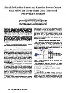
ABSTRACT The deregulation of the electrical market and the emergence of small energy production units connected to the distribution grid could induce a need on the one hand, to looped or to meshed some feeders and, on other hand, to control the active and or reactive power flows [1]. Series’ connected Flexible AC Transmission Systems (FACTS) devices can control active or reactive power flows in the transmission system in order to share the power between lines, to reduce line’s losses or to avoid overloads for instance [2][5]. The aim of this work is to develop the control of an inverter connected in series to the distribution grid: a Distributed Static Synchronous Series Compensator (D-SSSC). A safe and reliable novel method witch allows controlling the powers flows with no need to know line’s parameters is presented thanks to an automation approach.
INTRODUCTION
ACTIVE AND REACTIVE POWER CONTROL Distributed Static Series Synchronous Compensator (DSSSC) is a FACTS with weak active power capacity. Its structure is based on the Voltage Source Converter (VSC) where a capacitor is connected to the DC side of the device. The voltage level of the DC capacitor is regulated to its reference thanks to the active part of the voltage injected in series through the line. During this operation, the D-SSSC will act as a resistor/generator when a charge/discharge is need. The power flow through the line will be controlled thanks to the reactive part of the voltage injected. In this case the D-SSSC will act as a capacitor/inductor as the power flow through the line will be increased/decreased [5].
Amplitude current control The first step which leads to the power flow control is the current control. The control of the D-SSSC is synchronized with the line current thanks to a Phase Locked Loop (PLL), the voltage injected through the line will be ≤π/2 radians phase shifted. The current has to be expressed (through his amplitude) as a function of the reactive voltage injected through the line (vqVSC). The approach uses in this paper lead to exploit Concordia and Park transformations [6]. Then the electrical values of the simple network in Figure 1 are expressed in the rotating frame synchronized with the current in Equation 1. +
VS
Paper No 0667
for others; this implies, some time, non expected behaviours of the whole system. In the first part of this paper, the DSSSC is modelled with a perfect AC source. In the second part, the control of the DC bus voltage is studied with two control schemes which associate the control of the power flow and the control of the DC bus. In the last part, an experimental bench is used. Lab results are presented. These one are realized thanks to a real SSSC in series with a LV network, connected to dSPACE. This application translates Matlab/Simulink schematic into C code. This code is implemented on a real Digital Signal Processor (DSP) which controls the SSSC.
i
CIRED2007 Session 4
Joel GUIRAUD LEG / GIE-Idea – France
[email protected]
Vdc
FACTS devices such as the Unified Power Flow Controller (UPFC), the Interline Power Flow Controller (IPFC) and the Static Series Synchronous Compensator (SSSC) can realize Power Flow Control (PFC) thanks to their series-connected converter. This is done through an adjustable phase and amplitude voltage inserted to the line in series. The major goal of this system is then to control active and/or reactive power flow through the line, rather than the voltage injected. Thus, the desired power flow through the line should be ‘translated’ into the required injected voltage. Most of the theories on power exchanged with the line and those devices lead to complex and non-exploitable expressions. They cannot be used to choose controllers or even sizing them. In addition, some conclusions are contradictory as some researchers simply assumed that the active and reactive components of the injected voltage control respectively the active and reactive power flows [3], while others have found, through simulations, that the active power flow is more strongly coupled with the reactive component of the injected voltage rather than the active component [4]. First, in this paper, an approach used by control community is developed on the SSSC. This one leads to exploitable formulas that can be used to choose the appropriate controller. The non-specialists in control usually choose a Proportional and Integral (PI) controllers without looking
Raphäel CAIRE LEG / GIE-Idea – France
[email protected]
-
vVSC Rline/2 Rline/2
Rline/2
Lline/2 i
i Rload vfeeder
Erwan LE PELLETER LEG / GIE-Idea – France
[email protected]
Lload
Figure 1 – Simple grid with D-SSSC
Page 1 / 4
CIRED
19th International Conference on Electricity Distribution
Vienna, 21-24 May 2007 Paper 0667-
R + Rload = − line dt Lline + Lload
di dq
(
1 ω ⋅ i dq + ⋅ v dq feeder + v dq VSC Ll + Lch
)
Equation 1 Simplifications can be done as there is no iq value due to the synchronization of the rotation frame. This leads to the expression of the amplitude of the current as a function of vqVSC and vq_feeder in the Laplace domain. It can be seen that the transfer functions corresponding to vqVSC, the controllable variable and to the perturbation, vq_feeder, are the same. Theirs particularities are to be constant and equal to the inverse of the reactive part of the grid impedance (Equation 2). Iˆ( p ) = i d ( p ) =
1 1 ⋅v ( p) + ⋅v ( p) (Ll + Lch )ω qVSC (Ll + Lch )ω q _ feeder
Equation 2 The equivalent bloc diagram of the grid can be shown as the following Figure 2. vfeeder_q 1 ( Lline + Lload )ω
1 ( Lline + Lload )ω
vsq
+
id
The properties of the system have to be checked for a generalized looped grid index (n), see Figure 3, with m loads and where the D-SSSC is connected to the branch p. Rl2 i ch1
Ll2 il2
R ln Lln i ln R lp 2 Llp 2 i ch2
VVSC
Rlp 2 Llp 2 i
ichn
lp
R ln L ln iln i chp
R lm
L lm ilm R l(m+1) L l(m+1)
I chn
ichm
Vfeeder2
Vfeeder1
L l1 i l1
Figure 3 – Generalized meshed grid In the same way than the simplified grid, simplifications lead to the general expression, Equation 3:
Iˆ = il _ pd
VVSC _ q + V feeder1q − V feeder 2 q p −1 n n 1 = m +1 ⋅ − ∑ ∑ Rli + ∑ Ll i p ⋅ iload _ nq − Ll nω ⋅ iload _ nd i =1 Ll nω n =1 i =1 ∑ m m +1 n =1 m +1 + ⋅ iload _ nq − Ll nω ⋅ iload _ nd Rl + Ll p ∑ ∑ ∑ i i n = p i = p +1 i = p +1
Equation 3 Each load and each voltage feeder appears as a perturbation but the transfer function keeps his properties (Equation 4). Iˆ ( p ) = T (p ) = VS _ q (p )
1 m +1
∑
n =1
Equation 4
L l nω
The optimal controller can then be chosen in order to have, in closed loop, the expected operation of the whole system. As the system is a fixed admittance in open loop, if the corrector used is an integrator, it will become, in closed
CIRED2007 Session 4
H (p ) =
KI p 1 m +1 ∑ L ln ω 1 + p ⋅ n =1 KI
Equation 5
First order systems present advantages: the output value will never exceed the reference value and the control is realize smoothly as there is no oscillations.
Active or Reactive Power Flow Control The final goal of the system is to control active or reactive power. It is assumed that active and reactive power cannot be controlled at the same time as there is only one free controllable signal. So exploiting classic formulas of active and reactive power as a function of the voltage at the point of connection of the D-SSSC and the current through it, news expressions are obtained (Equation 6). Theses expressions are corrects as it is assumed that voltage variations are low in comparison of current ones (especially in looped or meshed grid).
n =1
Figure 2 – Bloc diagram of the grid
R l1
C I (p) =
P( p ) 3 V ⋅ cos ϕ = ⋅ max Vs _ q ( p ) 2 m +1 ∑ Ll nω
+
vqVSC
loop, a first order system (Equation 5).
Paper No 0667
Q( p ) 3 V ⋅ sin ϕ = ⋅ max V s _ q ( p ) 2 m +1 ∑ Ll n ω
Equation 6
n =1
Theses expressions will be opposed to experimental results, (last part of the paper).
DC BUS CONTROL Once, the rules of the power flow control have been set. The control of the DC bus device has to the done. Two methods are then proposed in the next section.
Parallel control scheme The first control of the DC bus voltage is realized by direct action on the active part of the injected voltage. The voltage injected through the line is an image of the modulating β (or u when discretized) as the VSC can be seen as an amplification of β varying between -1 and 1 (the signal to amplify) by the gain Vdc [6]. The first step is to express the current through the DC bus as a function of the active part of the modulator and the line current. See Equation 7. idc = i ⋅ β d < idc >=< i ⋅ u d > < idc >=
I max ⋅ u d _ max
Equation 7
2
This current flows through the DC bus which is modelled by a resistor (Rc) in parallel with a capacitor (C). The evolution of the voltage can be obtained (Equation 8). vdc ( p ) I ⋅R 1 = T ( p) = max c ⋅ u d _ max ( p ) 2 1 + Rc ⋅ C ⋅ p
Equation 8
Page 2 / 4
CIRED
19th International Conference on Electricity Distribution
Vienna, 21-24 May 2007 Paper 0667-
It can be seen that the system is a first order expression. To control it, a PI controller can be chose. With the compensation pole method, a first order system is obtained in closed loop (Equation 9) [6]. OLTF ( p ) = C ( p ) ⋅ T ( p ) = Kp ⋅
The controller is the same than in the parallel control scheme. However as the control of the DC bus voltage is an imbricate control scheme the inner loop must be faster than the external looped which control the power flow through the line (Figure 5).
1 + τi ⋅ p I max ⋅ Rc 1 ⋅ ⋅ 2 1 + Rc ⋅ C ⋅ p τi ⋅ p
ε
π/2
arcsin
- π/2 Grid
with linéarisation
τi = Rc ⋅ C
Vvsc
External control I
Vvsc_d_max_ref Grid’s operator I + ref or advance control algorythm -
I
| |
0.95*sin(ωt-sgn*(π/2)+γ)
Vdcref
1/0.95
ε
+
- π/2
Vdc
Imax
γsat
γ π/2
PI 1
-1
I
Equation 9 The parameter Kp will be choose in order to control the loading speed. However if this parameter is too high the apparent resistor of the system will reduce the current level (Imax) and make the load longer. The global scheme for a single phase D-SSSC associating both power flow and DC bus control is presented in Figure 4. From the single phase scheme, the three phase scheme can be simply deduced with udmax and uqmax directly send to a SV-PWM [6] block synchronized with the line current.
sin
PWM
IGBT control
sgn
ωt
Internal control
-
1 2τi 1+ ⋅p Kp ⋅ I max ⋅ Rc
+
CLTF ( p ) =
γ
PI
Vdc
PLL
Figure 5 - Single phase control synoptic of the D-SSSC – Inner loop control scheme
The three phase voltage control obtained from the single phase voltage control is easy to obtain. uqmax is set to ±1 there is an increase or decrease of the power flow and udmax is modulated continuously. These values are sent to the SVPWM and the saturators adapt uqmax.
EXPERIMENTAL VALIDATION
Grid Vvsc
PI
Vvsc_d_max_ref
0.95
Vvsc_q_max_ref
Vdc
sin
IGBT
/
1
uq_max
0.95 0
+
PWM control
sin u sin(ωt-sgn*(π/2)) q_max
sgn -1
I
PLL
Test device presentation
+
Vdc
| |
I
I
ud_maxsinωt
+
Grid’s operator I ref + or advance control algorythm Imax
ud_max -0.95
-
Vdcref +
Vdc
ωt
Figure 4 – Single phase control synoptic of the DSSSC – Parallel control scheme
Both controls (parallel and inner loop) which have been presented in the previous sections were implemented in a low voltage grid (Figure 6). The SSSC is in series with a load. DSpace control (Matlab/Simulink interface) Voltage Source Converter
Resistive and inductive load
Inner loop control scheme The previous control scheme implies a DC bus voltage always set to his reference whatever the level of compensation of the impedance of the line. This induces non-optimal functioning as excessive losses are produce and non-minimal Total Harmonic Distortion reached. The DC bus voltage is not adapted to the require voltage needed to realize the compensation. If the modulating β is always set to his maximum (amplitude close from 1) and the phase is shifted with the current by ≤π/2 radians (active power exchange null), an added phase shifting (γ) will create an active power exchange [5]. This will implies a non-null average current in the DC bus (Equation 10). Equation 10 I max ⋅ u max ⋅ sin γ 2 The charge/discharge of the DC bus will be as high as the adding phase shifting will be important. A new system can be obtained as γ is the controllable variable to Vdc. A linearization of sin is considered; this one is justified thanks to low adding phase shifting evolution or the use of a linearized control (arcsin function). The transfer function is the one presented in Equation 11 which is very close to Equation 8.
< idc >=
v dc ( p ) 0,95 ⋅ I max ⋅ Rc 1 = T ( p) = ⋅ γ ( p) 2 1 + Rc ⋅ C ⋅ p
CIRED2007 Session 4
Equation 11
Figure 6 – General overview of the SSSC
This one is decomposed into several parts: - a feeder (400/230V); - a physical SSSC is realized, thanks to a three phases VSC associate to a filter (Table 1); - a controller of the VSC is realized with dSPACE RTI1005. This device transforms Simulink schematics into C code exploitable by a DSP; - a load, which is a three phase commutable variable load of resistor (6kW) and inductor (6kVar). Parameters
Abreviation
Value
LC filter inductor
Lf
360 µH
LC filter capacitor
Cf
100 µF
Nominal apparent power
SN
10 kVA
Sample period
Ts
100 µs
Commutation frequency
Fc
10 000 Hz
DC bus max voltage
VDC
400 V
DC bus capacitor
Cbus
1100 µF
Table 1 – Parameters of the physical SSSC
Paper No 0667
Page 3 / 4
CIRED
19th International Conference on Electricity Distribution
Vienna, 21-24 May 2007 Paper 0667-
Parallel control scheme In Figure 8, the control of the DC bus to 400V can be observed (yellow: amplitude of the line current (A); blue: line current in phase 1 (A); green: voltage of the DC bus (V) and pink: voltage injected in series through the line (V)).
response as the active power flow naturally increases (yellow in Watt). The low evolution of the voltage in each part of the SSSC (pink and green in V) can be seen.
Figure 11 – Inner loop control scheme – Reactive Power Flow control to 700Var Figure 8 – Parallel control scheme – Control of the DC bus to 400V The characteristic response of a first order system to a step reference is observed. The system behaves like a resistor as it absorbs energy. This is why there is a diminution of the line current. In Figure 9 the control of the line amplitude current to 5A is presented. The characteristic response of a first order system can still be observed. The SSSC behave essentially as an inductor (see the phase shifting between the voltage injected and the line current).
CONCLUSION In this paper, a novel method to realize power flow control thanks to a SSSC has been presented. This is a simple and generic method. Inner loop control scheme is preferred to parallel control as there is less harmonics and losses generation. The viability of the control has been experimentally checks and gives good results. SSSC for PFC seems to be interesting in looped / meshed network but the protecting scheme as to be revised because of the increase of short circuit current. The SSSC could be used to decrease the short circuit current in order to be still compliant with actual protection scheme.
REFERENCES
Figure 9 – Parallel control scheme – Control of the line current to 5A
Inner loop control scheme In Figure 10, the inner loop control is presented where the line is compensated in order to increase the line current. It goes from 9A, where the system behaves like an inductor, to 11A where it acts as a capacitor. The DC bus voltage level is adapted in accordance to the series voltage needed for the compensation.
Figure 10 – Inner loop control scheme – Control of line current to 11A
In Figure 11, the reactive power flow control is presented. It is decrease (blue) to 800Var following a first order step CIRED2007 Session 4
Paper No 0667
[1] G. Celli, F. Pilo, G. Pisano, V. Allegranza, R. Cicoria, 2005, “Distribution Network Interconnection for Facilitating the Diffusion of Distributed Generation”, Proceeding of International Conference and Exhibition on Electricity Distribution, Turin, Italy. [2] N. Li, Y. Xu, H. Chen, V. Allegranza, R. Cicoria, 2000, “FACTS - Based Power Flow Control in Interconnected Power Systems”, Proceeding of IEEE Transaction on Power Delivery, vol. 15, No. 1, February. [3] K. Sedraoui, K. Al-haddad, G. Olivier, 2001, "A new approach for the dynamic control of unified power flow controller (UPFC)", Proceedings of IEEE Power Engineering Society Summer Meeting, Vancouver, Canada. [4] K. Sreenivasachar, S. Javaram, M. M. A. Salama, 1997, "Intelligent autonomous control of a unified power flow controller", Proceedings of Second International Conference on Power Electronics and Drive Systems, New-York, USA. [5] K. K Sen, 1998, "SSSC – Static Synchronous Series Compensator: Theory Modelling and Applications", Proceeding of IEEE Transaction on Power Delivery, vol. 13, No. 4, October. [6] G. F. Franklin, J. D. Powell, A. Amami-Naeini, 2005, Feedback Control of Dynamic Systems (4th), PrenticeHall International, United States of America.
Page 4 / 4