SLAC-PUB-12407
Active RF Pulse Compression Using Electrically Controlled Semiconductor Switches Jiquan Guo, Sami Tantawi Stanford Linear Accelerator Center 2575 Sand Hill Rd, Menlo Park, CA 94025 Abstract. In this paper, we present the recent results of our research on the ultra-high power fast silicon RF switch and its application on active X-Band RF pulse compression systems. This switch is composed of a group of PIN diodes on a high purity silicon wafer and has achieved a switching time of 300ns. The wafer is inserted into a cylindrical waveguide operating in the TE01 mode. Switching is performed by injecting carriers into the bulk silicon through a high current pulse. The RF energy is stored in a room-temperature, high-Q 375 ns delay line; it is then extracted out of the line in a short time using the switch. The pulse compression system has achieved a gain of 8, which is the ratio between output and input power. Keywords: RF switch, active pulse compression, PIN diode PACS: 84.40.-x
ACTIVE RF PULSE COMPRESSION Modern high gradient normal-conducting accelerator structures require very high power RF. To achieve the high power without adding expensive microwave tubes, RF pulse compression systems are commonly employed to match the longer pulses from the RF tubes with relatively lower power to the structures which require shorter but higher power pulses. Since the first RF pulse compression system for RF accelerator structures, SLED (SLAC Energy Doubler) [1] was introduced, several pulse compression schemes have been studied. Among them are BPC (Binary Pulse Compression system) [2] and SLED II [3]. Although BPC has 100% intrinsic efficiency, the system comprises a large assembly of overmoded waveguide, which makes it extremely expensive and large in size. The SLED II pulse compression system employs high Q resonance delay lines behind an iris to accumulate RF energy from the incoming pulse, and then the incoming pulse is reversed 180° in phase, so the reflected pulse from the input and the emitted RF from the delay line can add constructively to form a higher-power pulse. Such a resonant delay line pulse compression system is compact and is more efficient than SLED, but the efficiency deteriorates with higher compression ratio. The maximum power gain for a lossless SLED II system is 9 if the phase of the RF source can be flipped; for a system with an RF source unable to flip the phase, the maximum power gain is only 4. Active pulse compression systems using high power RF switches has been suggested to improve the efficiency of the resonant delay line pulse compression ___________________________________________
#
[email protected] *Work supported in part by U.S. Department of Energy contract DE-AC02-76SF00515
Contributed to 12th Advanced Accelerator Concepts Workshop (AAC 2006), 07/10/2006-7/15/2006, Lake Geneva, Wisconsin
system [4]. In an active system, the iris between the RF input and the resonance delay line is switchable, which allows the coupling coefficients of the iris to be optimized separately for the charging phase and discharging phase, so that the RF energy stored in the delay lines can be fully discharged in one delay cycle. Such a system requires a switch with low insertion loss, fast switching time and high power handling capacity. There is no intrinsic limit for maximum power gain in active compression systems, but the gain is limited by the amount of losses in the switch and the delay line. Several types of switches have been studied for active RF pulse compression systems, including ferromagnetic, ferroelectric, plasma and semiconductor switches. A semiconductor switch based on bulk effects has been demonstrated. This switch is based on the excitation of electron hole plasma on the surface of a semiconductor using a laser pulse [5]. To eliminate the laser from such a system, PIN diode junctions have been used to inject the carriers into the bulk of a semiconductor wafer [6]. Although the switch presented in [6] have shown a power handling capacity of 10MW with short pulses, it is too slow and lossy for practical application in active compression systems. In the rest of the paper, we will present the recent results of our research on the ultra-fast high power RF electrically controlled semiconductor switches. This switch demonstrated fast enough speed and low enough loss for active pulse compression applications, with 8 times power gain achieved. The process for the PIN diodes is compatible with the popular CMOS IC process, so the unit cost should be moderate if it’s produced in volume. The requirement of the driver for the solid state silicon switch is also lower than other options. A typical setup uses a 1kV 1kA pulsed power driver, while the plasma switches need about 100KV driver voltage, and the optical switch requires a costly high-power laser.
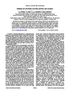
THE SWITCHABLE IRIS MODULE
Active window
∆Ψ
3 1
2
FIGURE 1. The tunable switch module
As discussed in the previous section, the active pulse compression system requires a switchable iris with certain coupling coefficients at charging and discharging phases. The optimized coefficients are functions of many variables such as compression ratio, losses in the delay line and at the iris. A tunable iris module was then designed to match coupling coefficients of the active window to desirable values at both on and off states. The module is composed of a Tee junction with the active window and a movable short plane connected to the 3rd port, as shown in Fig. 1. When the active window is turned on, it acts as a short plane and the phase of the reflected signal from the third-port changes. Hence, the coupling coefficients relating the remaining two ports are switched. These coefficients depend on the location of the active window, which determines the coupling during the on state, and the location of the movable short, which determines the coupling during the off state. A low-loss circular waveguide Tee junction has been specially designed and machined for our test setup. This Tee is composed of a TE20 mode rectangular Tee and 3 circular-to-rectangular mode converters [7], with S33=0.
PHYSICS AND DESIGN OF THE ACTIVE SILICON WINDOW Meta
SiO2
N
Metal
P Intrinsic
FIGURE 2. Cross-section of one PIN diode (not to scale) Recently, we have designed a new active switch window working in a circular waveguide. Like the switch Tamura and Tantawi developed in [6], this switch also works under TE01 mode. This mode has no radial electric field and azimuthal magnetic field; hence, a small gap in the waveguide will not lead to RF leakage without the choke structure. We have chosen the planar structure PIN diodes, with both P and N doping on the front surface of the silicon window. The cross-section of the diode is shown in Fig. 2. This structure makes shorter intrinsic region length possible, so the switching speed can be optimized. When the planar diodes turn on, the injected carriers concentrate near the top surface of the silicon wafer, which can help to reduce the RF losses. The switch stays off during the charging phase of the pulse compression system and turns on to discharge the pulse, which is opposite to the older Tantawi and Tamura design and helps to reduce losses in the charging phase and enhance switching speed. The design of the switch is optimized for working in 1.3 inch circular waveguide at 11.424GHz, same as the switch described in [6]. The working frequency is quite close to cutoff of the waveguide. This choice reduces the amount of required injectedcharges, but it compromises power handling capacity and increases losses.
Since both P and N doping regions are on the same side and the number of diodes is large, the biasing needs some special design. The positive biasing of each diode is provided by a metal line from the edge of the wafer. The metal lines providing negative biasing are extended out from a metal ring in the center, and the metal ring is connected to the outside by 24 metal lines instead of several hundred. The diodes only cover a ring between the waveguide wall and metal ring. The metal ring’s width and radius can be adjusted so that the window can be matched when the switch is off. This is very helpful in reducing the maximum field in the 3rd arm during the charging phase, and it also reduces the losses. More interesting is that this ring also helps the reflection of the RF signal when the switch is on; hence, it reduces the required amount of injected-carriers. Simulation with HFSS [8] shows that when the diodes are off, the window has 0.7% losses and 98% transmission coefficient. This assumes a 500µm thick silicon wafer with a 100KΩcm resistivity. Without the inner metal ring on the wafer, the reflection will be more than 80%. When the diodes turn on, eventually a carrier layer with 50 µm thickness and a density of 5×10¹⁶/cm3 is formed. This layer and the metal ring result in a transmission of less than 1% and power losses of about 10%. To achieve this carrier density, the switch needs about 70µC of evenly distributed carriers.
FIGURE 3. Fabricated Active Window We have simulated the time response of the diodes with the Medici code [9]. The dopant profiles of the devices used in Medici simulation were imported from the result of process simulation with TSuprem [10]. The actual process was optimized based on the simulation results as well as the test results from previous revisions. For planar structure diodes with 60µm length, which are connected in parallel, simulation shows that the average carrier density of the top 50 µm layer at center of the diodes will rise to 5×10¹⁶/cm3 after about 200 µC of charges injected. The length of the diodes is close to the carrier diffusion length in the silicon. This choice minimizes the non-uniformity of carrier distribution and maximized the efficiency of carrier injection. With a current source providing 1 KA pulse with 50ns rise time, the switch can be turned on in 250ns. The carrier lifetime is assumed to be > 100 µs. We have made such a switch; it is shown in Fig 3. The fabrication of the switch was completed at the Stanford Nanofabrication Facility by the author, with CMOS
compatible process. The switch was built on a Floatzone silicon wafer with 90K Ωcm resistivity and the thickness of 500 µm.
EXPERIMENTAL RESULTS We have characterized these switches with both network analyzer measurements and active switching tests; we performed the tests under the one-pass setup as well as the module setup with the switch attached to the circular Tee and a movable short. After that, we tested the switch in the active pulse compression system. In the one-pass network analyzer characterization, we have measured S12=0.90 and S11=0.35 with 6.5% loss, including about 1% losses over the mode converters and 2% over the holder. Active switching tests have been performed both with one-pass setup and the module setup. Peak RF power analyzer was used to measure the input and the transmitted/reflected power through directional couplers. The switch is powered by an IGBT circuit. With 700 V over the IGBT and the load, the current output can rise to 600 A in about 40 ns, and then rise to 1400A in 300 ns. A