General principles are illustrated with ... modeling RF, mixed signal and low-Vdd circuits (Vdd = 0.6- ... to erroneous results for the Gm/Id ratio (critical for analog.
Advanced Compact Models: Gateway to Modern CMOS Design (Invited) 1
G. Gildenblat1 , C. McAndrew2 , H. Wang1 , W. Wu1 , D. Foty3 , L. Lemaitre4 and P. Bendix5 Department of Electrical Engineering, The Pennsylvania State University, University Park, PA 16802 USA 2 Motorola Inc., Tempe, AZ 85284 USA 3 Gilgamesh Associates, Fletcher, VT 05444 USA 4 Motorola Inc., Geneva Switzerland 5 LSI Logic Corporation, Milpitas, CA 95035 USA A BSTRACT
Recent progress in MOS device physics, model development, and model implementation process has qualitatively changed the capabilities of compact models precisely at a time when the rapid expansion of RF MOSFET applications is imposing the most stringent demands on the new generation of MOSFET models. This work reviews the impact of the new modeling paradigm on MOSFET circuit simulation with particular attention to RF issues, non-quasi-static effects, and symmetric surface-potential-based models. General principles are illustrated with the simulation results using the latest generation compact MOSFET model (SP).
of this approach. However, recent reformulation of the chargesheet model using a symmetric linearization method [6] resulted in a model formulation which is no more complex than less accurate Vth -based or Qi -based models while producing results that are numerically equivalent to the original form of the φs -based model. Furthermore, the difficult problem of computing the surface potentials as functions of the terminal voltages has been solved by improving the convergence of the numerical algorithms and more recently using analytical approximations accurate to within 10 nV. The reported results were limited to the range adequate in bulk MOSFET models but a simple extension of the work in [7] [8] produces ana-
I. I NTRODUCTION
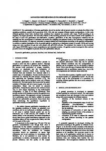
2.5 Analytical Approximation Iterative Solution
Surface Potential φs, V
2 V =1 V sb
1.5 0
1
−0.6
0.5
−0.8 0
−0.5 −1
0
1
2
3
Vgs−Vfb, V
Fig. 1. Surface potential computed using new analytical approximation and numerical iteration for different back bias; tox =3nm, Nsub = 1017 cm−3 . 1
Normalized Gate Capaciatnce
Until recently threshold voltage-based MOSFET compact models were considered standard and attempted to accommodate the increasing demands of the design community by a rapid increase in the number of model parameters without changing the regional nature of the model. This approach culminated in the development of the widely used BSIM3/4 models but is almost universally agreed to be inadequate for modeling RF, mixed signal and low-Vdd circuits (Vdd = 0.61.0V) envisioned by the National Roadmap for Semiconductor Technology. Some of the fundamental structural flaws of Vth based models include the use of source-referenced threshold voltage producing a singularity in the I-V characteristic, unphysical description of the moderate inversion region leading to erroneous results for the Gm /Id ratio (critical for analog designers) and inconsistent modeling of charges and currents producing negative transcapacitances [1] [2]. Hence there is a wide consensus for the need to replace Vth -based models with either inversion charge (Qi ) based [3] or surfacepotential-based [4] [5] models. The progress in this direction has brought about qualitative improvement in our ability to simulate CMOS circuits and is reviewed in this work. Since the source-drain overlap regions are critical in modern scaled devices we concentrate on the φs -based approach which is the only one allowing the physical modeling of these regions (where neither Qi nor Vth are useful variables).
0.8 Analytical Approximation Iterative Solution
0.6
−0.8
0.4
−0.6
0.2
0 0 −1
0
1
Vsb=1 V 2
3
Vgs−Vfb, V
II. D EVICE P HYSICS A SPECTS Traditionally, the development of φs -based models has been inhibited by the perceived difficulty (or at least complexity)
0-7803-8715-5/04/$20.00 ©2004 IEEE.
Fig. 2. Normalized C-V curves computed using new analytical approximation and numerical iteration for different back bias; tox =3nm, Nsub = 1017 cm−3 .
638
Saturation Threshold Voltage, V
Measured 0.14
0.135
0.13
SP
BSIM
0.125 0
2
4
6
8
10
Channel Length, µm
Fig. 3. Saturation threshold voltage is defined as the intercept of Vgs plot with horizontal axis; Vds =1.5V, W=10µm, Vbs =0V.
√
Id vs.
Fig. 4. Simple CMOS RF mixer. Besides the RF signals there are DC offsets to bias the MOSFETs ”on” and avoid forward biasing of source-bulk and drain-bulk junctions.
lytical approximations valid for extreme forward biases of the source/drain junction occasionally encountered in SOI devices. Typical results shown in Figs. 1, 2 demonstrate sufficient accuracy not only for φs but also for a much more demanding task of evaluating the transcapacitances. While not using the threshold voltage as a key variable, φs based models are capable of a very detailed modeling of Vth (defined in a suitable manner as a process characterization tool or as a design aid) as a function of geometry. In fact, as shown in Fig. 3, φs -based modeling of Vth (L) dependence may be superior to the traditional description.
−20
−40
e Fundam
IV. ACCUMULATION REGION AND EXTRINSIC MODELS A unique advantage of φs -based MOSFET models is the capability to describe the accumulation region with the same
IM3, B
SIM4 a
nd SP
−60
Vout (dBm)
−80
−100
−120
−140
−160
−180
−200 −50
III. M ODEL S YMMETRY A fundamental requirement of accurate MOSFET models is symmetry with respect to source-drain interchange (”Gummel symmetry” [9]). While any model can be made symmetric by forcing source-drain interchange in the code (i.e. by defining the drain as the terminal with higher potential) this procedure results in a singularity of the I-V characteristic at Vds = 0 if the model is inherently asymmetric. In models like BSIM3 or BSIM4 which use a source-based threshold voltage this behavior is inevitable [9] and prevents the modeling of thirdorder intermodulation terms (IM3) in pass transistors and passive mixers (commonly used in mobile communication systems). The details for the mixer shown in Fig. 4 are shown in Fig. 5. The singularity of the I-V characteristic of the ”standard” models results in the incorrect (2dB/dB) slope of the third order terms, while non-singular φs -based model (we use SP [4]) produces the correct slope. The second common cause of the singular behavior, the improper modeling of the velocity saturation effect [9], is for some reason present in the existing Qi -based models but does not seem to be inherent to this approach. The use of source-referenced threshold voltage and asymmetric bulk charge linearization in standard Vth based models not only violates the Gummel symmetry but prevents the modeling of common current division (”R2R”) circuits, which represents no difficulty for Qi and φs -based models [10] [11]. Both of these examples clearly illustrate the relation of the model structure to its simulation capabilities.
ntal BS
SP and M4 BSI , 3 SIM ic B mon Har 2nd M4 BSI and 3 M SI ic B mon Har 3rd P ic S on rm a H 3rd −45
−40
−35
−30
VRF
−25
BSIM3 BSIM4 SP −20
−15
−10
Fig. 5. Intermodulation products for the passive RF CMOS mixer circuit shown in Fig. 4.
set of equations that are used for other regions of the device operation. In particular, this means that separate varactor models are not always needed to model the voltage dependence of the oscillation frequency in voltage controlled oscillators [10]. Similarly, the availability of the surface potential in the source-drain overlap regions enables an accurate modeling of the bias-dependent overlap capacitances [12] and the innerfringing effects [13]. The latter represent a serious difficulty for the more traditional approaches to compact modeling [14]. The availability of the surface potential in the source-drain overlap regions also enables an accurate modeling of the gate tunnelling current in scaled MOS transistors [12]. V. L ARGE - SIGNAL NON - QUASI - STATIC (NQS) MODEL Analysis of the RF and mixed signal circuits often requires the inclusion of NQS effects. These can be modelled via a relaxation-time model [15] (often imprecise for the case of fast transients [1]), using the accurate but time-consuming segmentation method [16] or by solving the continuity equation [6], [17]. While potentially the most accurate the last approach has never been implemented in circuit simulators. More recently the application of the spline collocation method [6] allowed a practical version of this powerful approach. In this work the method described in [6] was generalized to include the accumulation region, combined with the SP quasi-static model [4] and implemented in Mica using RC subcircuits to solve the
639
differential equations of the spline collocation method. Typical results for the charge pumping depicted in Fig. 6 are shown in Fig. 7 and clearly show NQS effects. Drastic NQS effects for the digital-to-analog converter shown in Fig. 8 are presented in Fig. 9. The new version of the spline collocation NQS model has been verified by comparison with the numerical solution of the continuity equation [6], [17] �� � � ∂ qi kT ∂qi ∂qi + − =0 (1) ∂t ∂y ∂qi /∂φs q ∂y where qi is the inversion charge per unit channel area, φs is the surface potential, the normalized coordinate y is counted from source towards the drain, time t is normalized to L2 /µ, µ is the effective channel mobility and L is the channel length. Typical results shown in Fig. 10 illustrate the high accuracy of the NQS model. 5V
-5V
R=100MΩ 1V
+ −
Fig. 9. The simulated output current of the DAC cell with an input ramp rate of 5V/1ns.
VG Iout
Iin Cin=0.1pF
Cout=1pF
Fig. 6. Schematic diagram of the switch capacitor circuit used for simulation. L = 5µm, Tox = 8nm, Nsub = 2 × 10¹⁷ , µ = 500cm2 /V s.
Fig. 10.
Current Transients for the linear region operation.
VI. R APID DEVELOPMENT AND IMPLEMENTATION OF COMPACT MODELS USING V ERILOG -A
Fig. 7. Error voltages at the source and drain nodes of the switch capacitor circuit.
Vdd
S
M3p
M4p
Mtp
S M2p
M1p
Mbp M1n
M2n
Iout
6mA
Most compact models are implemented in circuit simulators in a low level language like C, and for a typical MOSFET model this requires around 20,000 lines of code. Generation of this code, which includes manual coding of the derivatives needed by the Newton like algorithms in most circuit simulators is a non-value-added, error prone and tedious task. It is also a barrier to code re-use and sharing, and a barrier to the introduction of new and enhanced features to a model. In the past years a significantly better approach has become accepted, where a model is defined in a high level language, Verilog-A, and the low-level C code is automatically generated from Verilog-A, including symbolic generation of derivatives [18]. Not only does this reduce model definition from tens of thousands of lines of code to several hundred, and gives much more readable code, but it gives correct-by-construction derivatives (incorrect derivatives are the most common source of errors in manually coded compact models). Fig. 11 shows a high-level view of how ADMS, the system used to generate code for SP, operates. VII. S TATISTICAL M ODELING
Fig. 8.
Schematic diagram of a DAC cell.
Historically corner (or ”skew”) model files have been the cornerstone of statistical simulation for IC design. This worked
640
cesses and modern circuit design methods. Surface potentialbased models provide both the most physical and practical foundation for the next generation general-purpose compact MOSFET models. ACKNOWLEDGMENT This work is supported in part by the Semiconductor Research Corporation (contracts 2000-NJ-796 and 2000-NJ-997). The authors are grateful to W.-K. Shih, B. Mulvaney and S. Hamm for several illuminating discussions. Fig. 11.
R EFERENCES
ADMS XML based generation of code from Verilog-A.
0.8
Vth2 (V)
0.7 0.6
W/L=0.3/0.15µm
0.5 0.4 0.3 0.2
W/L=25/25µm 0.3
0.4
0.5 V
th1
0.6 (V)
0.7
0.8
Fig. 12. Measured threshold voltages from NMOS pairs of two geometries, from a 0.13mm CMOS technology. Different symbols are different wafer lots.
reasonably well for digital CMOS circuits, and not as well for analog ICs. However, there is a fundamental shift in the underlying cause of statistical variations in modern technologies [19]. Robust design requires accurate statistical simulation, so next generation MOSFET models must be able to accurately model statistical variations. Fig. 12 compares threshold voltages measured from two adjacent NMOS devices, over 13 wafers. The data at the lower left are for wide/long devices, and at the upper right for narrow/short devices. Clearly for the big devices the statistical variation is smaller than for the small devices. However there is also a change in the correlation structure, and it is apparent that for the small devices the local (or mismatch) component of variation is dominant. This component is uncorrelated between devices, which is inconsistent with corner file simulations, as they assume perfect correlation between devices. To enable accurate statistical simulation, MOSFET models need to be based on physical process parameters, and need to include both instance specific mismatch variation as well as global parameter variations. This is not just important for analog IC simulation, it is becoming important for digital CMOS simulation. VIII. C ONCLUSIONS New generation compact MOSFET models have solved several long-standing problems of compact MOSFET modeling. The general consensus is that traditional Vth -based models are outdated and are incompatible with advanced fabrication pro-
[1] W. Liu, MOSFET Models for Spice Simulation, Including BSIM3v3 and BSIM4. John Wiley & Sons, 2001. [2] P. Bendix, “Detailed Comparison of the SP2001, EKV, and BSIM3 Models,” in International Conference on Modeling and Simulation of Microsystems, April 2002, pp. 649 – 652. [3] M. Bucher, C. Lallement, C. Enz, and F. Krummenacher, “Accurate MOS Modelling for Analog Circuit Simulation Using the EKV Model,” in IEEE International Symposium on Circuits and Systems, vol. 4, no. 12-14, May 1996, pp. 703–706. [4] G. Gildenblat, H. Wang, T.-L. Chen, and X. Cai, “An Advanced Surface-Potential-Based Compact MOSFET Model,” IEEE J. Solid-State Circuits, 2004 (in press). [5] R. van Langevelde, A. J. Scholten, and D. B. M. Klaassen. (2002, Dec.) Philips MOS Model 11. [Online]. Available: http://www.semiconductors.philips.com [6] H. Wang, T.-L. Chen, and G. Gildenblat, “Quasi-Static and Non-QuasiStatic Compact MOSFET Models Based on Symmetrically Linearization of the Bulk and Inversion Charges,” IEEE Trans. Electron Devices, vol. 50, no. 11, pp. 2262–2272, Nov. 2003. [7] T.-L. Chen and G. Gildenblat, “Analytical Approximation for the MOSFET Surface Potential,” Solid-State Electronics, vol. 45, no. 2, p. 335, Feb. 2001. [8] W. Wu, T.-L. Chen, G. Gildenblat, and C. C. McAndrew, “PhysicsBased Mathematical Conditioning of the MOSFET Surface Potential Equation,” IEEE Trans. Electron Devices, 2004 (in press). [9] K. Joardar, K. K. Gullapalli, C. C. McAndrew, M. E. Burnham, and A. Wild, “An Improved MOSFET Model for Circuit Simulation,” IEEE Trans. Electron Devices, vol. 45, no. 1, pp. 134–148, Jan. 1998. [10] G. Gildenblat, T. Chen, X. Gu, H. Wang, and X. Cai, “SP: An Advanced Surface-Potential-Based Model,” in Proc. IEEE Custom Integrated Circuits Conference, 2003, pp. 233–240. [11] D. B. M. Klaassen, R. V. Langevelde, and A. J. Scholten, “Compact CMOS Modeling for Advanced Analogue and RF Applications,” IEICE Transactions on Electronics, vol. E87-C, 2004 (in press). [12] X. Gu, T.-L. Chen, G. Gildenblat, G. Workman, S. Veeraraghavan, S. Shapira, and K. Stiles, “A Surface-Potential-Based Compact Model of NMOSFET Gate Current,” IEEE Trans. Electron Devices, vol. 51, no. 1, pp. 127–135, Jan. 2004. [13] G. Gildenblat, X. Cai, T.-L. Chen, X. Gu, and H. Wang, “Reemergence of the Surface-Potential-Based Compact Models,” in IEDM Tech. Dig., 2003, pp. 36.1.1– 36.1.4. [14] D. Foty, MOSFET Modeling With SPICE: Principles and Practice. Upper Saddle River, NJ: Prentice Hall PTR, 1997. [15] M. Chan, K. Y. Hui, C. Hu, and P. K. Ko, “A Robust and Physical BSIM3 Non-Quasi-Static Transient and AC Small-Signal Model for Circuit Simulation,” IEEE Trans. Electron Devices, vol. 45, pp. 834– 841, 1998. [16] A. J. Scholten, L. F. Tiemeijer, P. W. H. D. Vreede, and D. B. M. Klaassen, “A Large Signal Non-Quasi-Static MOS Model for RF Circuit Simulation,” in IEDM Technical Digest, 1999, pp. 5–8. [17] C. Turchetti, P. Mancini, and G. Masetti, “A CAD-oriented Non-QuasiStatic Approach for the Transient Analysis of MOS ICs,” IEEE J. SolidState Circuits, vol. 21, pp. 827–836, Oct. 1986. [18] L. Lemaitre, C. McAndrew, and S. Hamm, “ADMS: Automated Device Model Synthesize,” in Proc. IEEE Custom Integrated Circuits Conference, 2002, pp. 27–30. [19] C. McAndrew and P. G. Drennan, “Unified Statistical Modeling for Circuit Simulation,” in Tech. Proc. of 2002 International Conference on Modeling and Simulation of Microsystems (MSM’02), San Juan Marriott Resort & Stellaris Casino, Puerto Rico, U.S.A., 2002, pp. 715–718.
641