system, hardware and physical design but have yet to encompass the complete problem. Some attempt to close the gap between algorithm and hardware ...
An Automated Design Flow for Low-Power, High-Throughput, Dedicated Signal Processing Systems W. Rhett Davis, Ning Zhang, Kevin Camera, Dejan Markovic, Tina Smilkstein, Nathan Chan, M. Josie Ammer, Engling Yeo, Borivoje Nikolic, Robert W. Brodersen Berkeley Wireless Research Center, Dept. of EECS, University of California, Berkeley Table 1: Architectural Comparison of Energy Efficiency for Common Methods of Algorithm implementation, Scaled to a 0.18 µm Technology
Abstract A system-level perspective of a hierarchical automated design flow for low-energy direct-mapped signal processing integrated circuits is presented. Capturing design decisions in a dataflow graph allows push-button automation of layout and performance estimation. A detailed example of the design process for a DSSS TDMA baseband receiver is presented.
1
64-point FFT Energy per Transform (pJ) Direct-Mapped Hardware FPGA Low-Power DSP High-Performance DSP
Introduction
The architectures commonly used to implement signalprocessing algorithms in hardware differ most significantly in terms efficiency and flexibility. General purpose processors are the least energy and area efficient, while slightly more specialized architectures, such as programmable digital signal processors, can often accomplish the same task with an order of magnitude less energy. The most efficient architectures in terms of power and area can be obtained by directly mapping the algorithms into hardware. Computational energy and area efficiencies that can be achieved with this approach are 100-1000 MOPS/mW and 100-1000 MOPS/mm2 . These efficiencies can be 2 to 3 orders of magnitude higher than the efficiency achieved by software processors [1].
1.78 683 436 1700
16-State Viterbi Decoder Energy per Decoded bit (pJ) 0.022 5.5 19.6 108
Direct-mapped architectures are seen as unattractive primarily because the tremendous design effort involved is not economically viable given the lack of flexibility of the final hardware. We have developed a solution for achieving the benefits of direct-mapping with drastically reduced design effort. A description of the physical design and software aspects of this flow has already been presented [4]. This paper presents a system-level perspective of our flow. The paper begins with a survey of existing methodologies in the context of how they can help. Then we present the user perspective that we want for our tool and a design example of a TDMA baseband receiver.
2
A direct-mapped architecture can be obtained by mapping the operations of a dataflow graph directly into functional units and hard-wiring the connections between them. In this way, the maximum parallelism can be obtained, allowing the minimum clock rate and supply voltage to be used, resulting in reduced energy per operation [2]. The ability to exploit a high level of parallelism allows computational rates that far exceed uniprocessors without requiring high clock rates. This efficiency makes directmapping attractive for many digital signal processing (DSP) applications. DSP algorithms can be extremely complex with very high processing rates but are highly parallel. Consider the performance of direct-mapped architectures compared to FPGA and programmable DSP implementations of the FFT and Viterbi decoder algorithms, two important parts of the IEEE 802.11a wireless networking standard. Table 1 shows the comparison between vendor-published benchmark data for the industry-leading high-performance and low-power programmable DSP’s and FPGA and post-layout simulations of direct-mapped hardware [3]. The results were calculated for constant throughput rates of 50 Ms/s for the FFT and 100 Mbps for the Viterbi decoder and have been scaled to a common technology (0.18 µm) to support a meaningful architectural comparison. The table shows roughly a 3 orders of magnitude energy penalty for the high-performance programmable approach and more than 2 orders of magnitude for the low-power approaches.
Current Methods for Algorithm Implementation
A standard design flow for hardware implementation of algorithms has four phases which are typically handled by four different designers. Algorithm designers conceive the chip and deliver a specification to system designers, often in the form of a floating-point simulation. This simulation can be used to generate system characterizations such as a bit-error-rate vs. signal-to-noise ratio (BER vs. SNR) curve for a communications chip. The system or architecture designers begin to add structure to this simulation, partitioning the design into functional units. They must also convert the data types from floating to fixed-point and verify that finite word-length effects and pipeline depth do not compromise the algorithm. The hardware (or frontend) designers map the simulation to register-transfer level (RTL) code (usually VHDL or Verilog) and verify that the code matches the specified functionality and pipeline depth. Physical designers take standard-cell netlists synthesized from the RTL code and use place-and-route tools to generate layout mask patterns for fabrication while verifying that all timing constraints are met, commonly referred to as reaching timing closure. This flow requires 3 translations of the design, expressing the functionality as gradually less sequential and more structural with requirements for re-verification at each stage. Opportunities for algorithmic modifications to reduce power and area are often lost due to the separation of engineering decisions. Performance bottlenecks discovered during the physical design phase are unknown to the algorithm designer. Aggressive system requirements may require new and unusual architectures, which can stall the flow, leading to uncontrolled looping back to earlier stages
In spite of the enormous advantage of direct-mapped architectures, they are not commonly used unless the application cannot be accomplished by any other means.
1
of the design process and extending the design time indefinitely.
Signal Decisions specifying the types for physical signals are captured as edge properties in the dataflow graph. Typically a behavior is specified with floating point types. Designers then seek to implement the same behavior with as few bits as possible. To aid this exploration, the designer is allowed to specify a signal as any 2’scomplement or sign-magnitude fixed-point type. To support mixed-signal design, a floating point type is considered an analog signal.
The main problem with this flow is that it attempts to avoid feeding back information to algorithm designers. The technique of reducing power through algorithmic transformations to permit voltage reduction [2] is well understood. However, today’s CAD environments do not support this kind of design. The flow we need would allow algorithm designers to explore the design space as thoroughly as possible by creating mask layout and obtaining performance estimates. This exploration should allow refinement of fixed-point types, be constrained by libraries of efficient hardware blocks and be carried out by an automated design flow. This encourages feedback of physical design issues to algorithm designers by allowing them to maintain ownership of the design data at all times. It also would encourage interaction with system, hardware and physical designers by reducing the design process to a single phase.
The flow recognizes certain primitives as re-ordering of wires to save power and area. For example, disabling a block in the simulation corresponds to a gated clock in the physical design. Simpler optimizations include multiplication by a constant power of 2 (a hard-wired shift) and comparison to zero (the sign bit). Circuit Decisions specify the transistors used to implement each block and are captured as node properties. Detailed architectural control may be necessary to optimize a massively parallel critical path. Through these decisions, designers should be able to explore the energy/delay/area trade-offs of different circuit topologies such ripple-carry vs. carry-lookahead adders or SRAM’s vs. flip-flops as storage elements. Other opportunities for exploration include the use of 4-to-2 compressors to speed up addition of many numbers or the substitution of CORDIC blocks for multipliers. Designers are also allowed to specify the supply voltage that they want for each block.
Recent efforts have identified the gaps between algorithm, system, hardware and physical design but have yet to encompass the complete problem. Some attempt to close the gap between algorithm and hardware design by basing synthesis tools on C/C++ descriptions [5]. However, these solutions encourage a sequential description of the algorithm and make it difficult to express the parallelism that would allow lowering the supply voltage. Commercial tools from design automation companies offer RTL code generation solutions from block diagrams. However, these tools are targeted mostly for hardware designers and obscure the information about the algorithm and architecture through the code generation process. A design environment is needed which offers fast, automatic generation of physical information from an algorithmexploration environment.
3
Floorplan Decisions specify the designer’s vision for the chip’s physical structure. Our flow limits these decisions to the drawing of standard-cell rows for placement and the manual placement of certain instances and boundary pins. Capturing these decisions in a dataflow graph is difficult, and so a companion floorplan view is created with commercial physical design tools. Based on these decisions, the designer may request performance estimates from the automated flow. The method used for estimation should depend on how many decisions have been made and how much time and diskspace the designer is willing to spend. Once function and signal decisions have been made, quick block-level estimates can be made, or the designer can request that an RTL estimation tool be launched. Once circuit decisions have been made, gate-, switch-, and transistor-level analyses are possible. After floorplan decisions have been captured, mask-layout can be generated, and parasitic wire capacitances can improve these estimates.
Chip-in-a-Day Design Flow
The goal of our flow is to make it possible to get mask layout and performance estimates for an algorithm in less than one day. The generation of the layout is automated from a dataflow graph that defines a direct-mapped architecture. In this section, we define the desired perspective for users of our flow.
3.1 Essential Design Decisions Commercial tools give designers many degrees of freedom, but it is this freedom that makes them hard to use. Designers are often forced to make decisions that are concerned more with running the tools than they are with optimizing their algorithms. For example, it would waste algorithm designers’ time to force them to choose how many passes a router attempts before failing. In order to reduce design time, we limit the types of decisions that designers are expected to make to the following: function, signal, circuit, and floorplan decisions.
3.2 “Push-Button” Automation Once the essential design decisions have been made, we want to deliver layout and estimates with “push-button” ease. This means that we want to provide automation similar to what is obtained with the programming tool MAKE. Our flow is described as a dependency graph, and tools are executed incrementally to update the desired targets. This means that no decisions can be made after the button is pushed.
Function Decisions specify the basic input-output behavior of a system. Because the interactions between units of behavior are often complex, these decisions are typically captured by tweaking and re-simulating the dataflow graph. Our flow considers the behavior of the dataflow graph with a certain simulator to be the final specification of behavior for the system.
“Push-button” automation further implies that there is no translation of design data. A well-automated flow does not force a designer to express a decision more than once. Doing so constitutes a translation of one decision into another, which is essentially what we are trying to avoid.
2
For example, an early version of our flow created a pad for every top-level port in the dataflow graph. However, in order to view a signal inside a dataflow graph, it was necessary to create an output port for the signal. As a result, designers would maintain two copies of the dataflow graph, one for simulation and one for generating layout with the flow. This required continual translation between the graphs, which slowed the design process considerably. Today, the flow allows the tagging of certain signals and blocks as “simulation-only” so that no translation is required.
language [7], which allows referencing and assigning variables inside the states. Input and output variables in the state-machine are input and output ports in the dataflow graph. Internal variables are part of the state. Lastly, because designs can become huge and complex, we need the dataflow graphs to be hierarchical. There are two main aspects of hierarchy that we want to capture: the grouping and referencing aspects. The grouping aspect is simply that certain parts of the dataflow graph should be grouped together so that the entire design need not be viewed at once. The referencing aspect is that a group can be referenced multiple times. This means that changes to the group need not be replicated to all of the references.
3.3 Dataflow Graph Description We would ideally like our dataflow graph to be used for algorithm exploration as well as for mapping to hardware. We would like to support the generation of BER vs. SNR characteristics, for example, which often requires simulation for many millions of cycles. In order to support fast simulation, our dataflow graph description needs to model hardware as abstractly as possible.
There are a number of dataflow graph editors that support the discrete-time model, and we chose MathWorks’ SimulinkTM [8] because of its familiarity to algorithm designers, due to its close integration with MatlabTM. It is important to make it as easy as possible for algorithm developers to approach the design environment in order to ease the use of hardware dependent optimization early in the design process. Figure 2 illustrates a cycle-accurate dataflow graph example of a time-multiplexed FIR filter. Figure 2(a) shows a multiply-accumulate block being fed
Conversely, if we want to eliminate translation of design decisions from our flow, then we must be able to verify the final hardware using the dataflow graph. The verification process must be defined in a way that is easily and robustly automated, since manual verification is prone to error. The verification requirement drives us towards less abstraction of the hardware.
2 TAP_COEF
D A
Q
WEN
To balance the needs for simulation speed and verifiability, we chose a discrete time computation model [6] for our dataflow graph simulator. We define our verification strategy as shown in Figure 1. The discrete cycleboundaries model the rising edge of the clock. The behavior of a discrete-time system can be described with a series state-updates and output-updates. The state of the system models the outputs of rising-edge triggered flipflops. The outputs of the system model the outputs of a network of combinational logic that follows the flip-flops, which settle to a final value after some circuit delay and glitching. Thus, the discrete states must match over the entire cycle, and the outputs must match at the instant before the cycle-boundary. This verification strategy requires that the dataflow-graph be cycle-accurate and bittrue with respect to the hardware. Cycle
1
2
A wen
1 X
B
Z
1 Y
RESET
reset_acc
MAC
CONTROL
(a) 1 A
2 B
+ MULT S12
1 Z
+ ADD S18
1 Z
REG
3 RESET MUX 0 CONST S18
3 (b)
Clock (Dataflow Graph) State
X1
X2
X3
(Hardware) State
X1
X2
X3
(Dataflow Graph) Output
Y1
Y2
Y3
(Hardware) Output
SRAM
addr
Y1
Y2
init entry: addr=0; wen=1;
Y3
[addr==15]
Figure 1: Dataflow-graph-to-hardware verification incr during: addr++; reset_acc=0;
A discrete-time dataflow graph uses arithmetic primitives such as add and multiply and state-primitives such as unitdelay blocks. Using such primitives, it is easy to model datapath logic. However, datapath logic generally requires a certain amount of control, which is difficult to model with dataflow primitives. Therefore, our dataflow graph needs a finite state-machine primitive that can be verified with the same strategy used for the datapath logic. We use an extended finite state machine based on the StateCharts
restart entry: addr=0; wen=0; reset_acc=1;
(c) Figure 2: (a) Dataflow graphs of a time-multiplexed FIR Filter with (b) a detail of the multiply-accumulate block and (c) detail of the control logic finite state-machine.
3
by an input data stream, tap coefficients from an SRAM and some control logic. Figure 2(b) shows a detail of the multiply-accumulate designed with datapath primitives. Figure 2(c)shows the address generator and MAC reset control state-machine. This chart has an initial loop to load tap coefficients, with successive loops reading the coefficients and resetting the accumulator.
receiver RF oscillators appear as a gradual rotation of the QPSK constellation. When the frequency is locked, a phase offset of the constellation is caused by phase-noise in the oscillators as well as the time-varying channel. Timing offsets appear as a gradual change to which of the 8 input streams is the best, caused by offsets in the frequency of the transmitter and receiver baseband clocks as well as timevarying delay through the channel. Each of these quantities (frequency, phase, and timing) must be estimated, corrected, and tracked for the system to work.
3.4 Translating Structure and Semantics The structure of the dataflow graph hierarchy is mapped into hardware automatically. The leafcells of this structure are called “macros”. A macro is a unit of hierarchy with a “generator” specified, which determines how the semantics of the underlying system are to be used. For example, control blocks are specified as state-machine macros, causing them to be translated into synthesizable VHDL by a tool we developed. For datapath blocks, our flow provides a fundamental library of datapath primitives which are mapped directly to RTL code for synthesis. However, this library does not permit the kind of datapath architecture exploration that we want to provide. Therefore, we use a datapath generator [9] tool for this kind of exploration. This generator uses primitives that are very similar to dataflow graph primitives, and ultimately we want to translate synthesizable code from the dataflow graph automatically, as we do with state-machines. At the present, this translation is done manually.
4
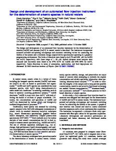
A block-diagram of the system is shown in Figure 3. The purpose of each block can be understood in terms of the role it fulfills in the locking sequence. Re-synchronization is performed at the beginning of every packet, which is at least 512 symbols long. • The coarse timing acquisition block correlates three of the eight streams with the known spreading code until one of them passes a threshold. The control block then selects this stream through a bank of multiplexers. This estimates timing to within 3/8 of a chip and needs at least two symbols (62 chips) to complete. • The frequency estimation and fine-timing block uses the chosen stream and its two nearest neighbors to estimate the frequency and further estimate the timing to the best of the three streams. This block requires 15 symbols to complete. • The rotate-and-correlate blocks multiply the three input streams by a rotating phasor using the frequency estimate from the previous block, correcting the frequency mismatch. This block also correlates each stream with the spreading code and monitors them to track timing by changing the current stream if necessary. • The best stream is passed to the PLL which takes at most 19 symbols to estimate the phase, at which point it corrects the phase and starts to track frequency and phase offsets. The entire system was drawn as a dataflow graph and implemented with dedicated logic. The two largest blocks in this system are the coarse timing block, which is active less than 1% of the time, and frequency estimation block, which is active 3% of the time. These blocks are therefore disabled (clocks are gated) by the controller when not in use to save power.
Design Example
This section describes the experience of one designer who used our flow to build a low-power, spread-spectrum TDMA receiver. The designer spent one year learning about communication theory while working with others to define a wireless system for sensor networks [10]. She had assembled floating-point simulations in a matrix math package for the digital baseband portion of the system and then decided to use our flow to implement her chip.
4.1 System Overview The chip was intended for a TDMA system with a length 31 direct-sequence code to spread the spectrum and provide resistance to narrow-band fading. The chip-rate of 25 MHz gives a symbol rate of 806 kHz, which translates to 1.6 Mb/s data rate with QPSK modulation. In-phase and quadrature (I and Q) samples from an A/D Converter are fed into the chip as 7-bit streams at 200 MHz, corresponding to 8 samples per chip, each offset by oneeighth of a chip. The job of the baseband receiver is to provide coherent timing recovery for the input stream.
4.2 Design Effort The first 8 months of the design process were spent implementing data-path macros. This involved design of 13 datapath generator macros described in 2000 lines of code. The system designer created all macros by herself
The task for this chip is to lock frequency, phase, and timing. Frequency offsets between the transmitter and I&Q Input
8
3 MUX 3
Coarse Timing Acqisition
Frequency Estimation and Fine Timing
Rotate and Correlate
Hard Symbols PLL
Control
Figure 3: Block Diagram of the Baseband Receiver
4
Soft Symbols
except for the primary Coarse Timing and Acquisition macro (500 lines), which was designed by another team member in 3 months. Most of this time was spent developing dataflow graphs along with datapath generator code and co-simulating to ensure equivalency. One statemachine with 20 states was designed at the same time to control the entire system.
L2 cache, 4GB of RAM, 8GB of swap, and a NetApp F630 filer available over Gigabit Ethernet. Table 2: Automated flow execution statistics Execution Time Disk Space Synthesis 1 hour 11 MB Routing 13 hours 330 MB DRC & LVS 3 hours 480 MB Clock Tree Verif. 13 hours 1.2 GB Other 11 minutes 350 MB Total 30 hours 2.4 GB
After the macros were complete, another 3 months were spent incorporating a series of changes: • RF Front-end was changed, necessitating earlylate correlators and tripling the size of the roateand-correlate blocks as already shown in Figure 3. No new library blocks were designed. • Interface spec to protocol chip and RF Front end were changed: 2 new datapath macros (100 lines of code), 1 new state-machine (4 states) • Spreading codes were made programmable: 1 new datapath macro (60 lines of code), 1 new state-machine (8 states) • Transmitter was added to the same design: 1 new datapath macro (300 lines of code), 1 new statemachine (8 states) • Additional testing capability was added: 1 new datapath macro (80 lines of code) These changes were incorporated by modifying the dataflow graph only. No modification to existing library elements was required. This means that design was done at a level higher than RTL. The designer said that the dataflow graph editor provided much more sophistication for analyzing the output of the system than an RTL simulator. Outputs could be easily interpreted as rotating phasors, complex vectors, or power spectra instead of simply bit vectors, accelerating her analysis of the system.
Total design time was 13 months. However, given these execution times, we see that the “chip-in-a-day” goal is not far from being possible. If the flow had not been under development, we project that the design time could have been reduced by several months. Furthermore, if library development had not been necessary, many more months of effort could have been eliminated. However, we have not yet used a library element on more than one chip without modification. This is due to the fact that the flow was being built and little time has been available for library support. Reuse of these complex blocks will be necessary to meet the “chip-in-a-day” goal. Even though reuse on separate chips has not yet been demonstrated, reuse inside the chip has accelerated the design process. The CORDIC-slice macro shown in Figure 4 was parameterized in terms of the bit-widths of inputs X, Y and A, the constant shift value G and the constant arctangent value T. The slice was then used 27 times with different parameters to implement CORDIC angle rotation and polar-to-rectangular conversion blocks. Once the CORDIC function was debugged and verified, no further debugging at the RTL level was necessary.
Routing passes and performance characterization for the macros began after 2 months into the project and were repeated periodically until the design was completed. These passes were initially done to determine critical-path delays, power consumption, and routed area of the design. As months progressed and the top-level floorplan became more definite, they were used to help determine the routability of the design and were repeated whenever a block changed size significantly. The designer estimates that each part of the design was re-routed between 5 and 15 times over the life of the project.
+ X X
sel neg
{g=i}
-/+
shift
+
shift
+
g sel +/-
sel neg
Y
Y
+ {t=tan -1(2 -i)}
-/+
t
sel neg
A
After the functionality of the dataflow graph was finalized, one month was spent running functional simulations to verify that the flow was working properly. Switch-level simulation was used because transistor netlists for the entire system were provided as a by-product of the flow. Several bugs in the flow were fixed, but no modification to the dataflow graph design data was required. This means that complete system simulations below the dataflow-graph level were a part of the flow development process, not a part of the chip design process.
+ A
+
Figure 4: Reusable CORDIC slice
4.3 Verification by Simulation Even though complete system simulations below the dataflow-graph level were not part of the design process, there were a number of difficulties that had to be overcome to ensure that the dataflow graph descriptions are cycleaccurate and bit-true.
Once the functionality of the hardware was verified, one month was spent inserting the clock tree, routing, and physically verifying the blocks. This process was delayed because the clock-tree insertion portion of the flow was still being developed. For each pass of the flow, the execution time and disk space required are given in the Table 2, shown for a 400 MHz UltraSPARC-II system with 2MB of
One problem was bit errors with constant shifts. Figure 5 shows what we expect in hardware and what the dataflow graph simulator produced. This error appeared for negative numbers only and was therefore difficult to find. To fix this problem, we created our own dataflow graph primitive which gave us the correct behavior.
5
windows” as illustrated in Figure 7, we may be able to relax the constraint that the pipleline depth of the hardware and dataflow graph match. These simplifications could speed up simulations considerably.
Hardware Behavior - Correct 1 0 1 -3
>>1
1 1 0 -2
Cycle
Dataflow Graph Behavior - Incorrect 1 0 1 -3
2
1 1 1 -1
5
Another problem was a discrepancy between the behavior of a gated clock and the dataflow-graph enable function. This discrepancy was due to the fact that in the dataflowgraph simulator, the output is not updated until the cycle after the state is updated. Thus, if a block’s state changes and is then disabled on the next cycle, the output will not be updated until the block is re-enabled. This differs from hardware, because the output is always updated when the state changes.
3
4
5
6
Dataflow Graph D1
D2
D3
D4
D5
D6
Hardware
D2
D2
D2
D3
D4
D1
Conclusion
The success of the baseband receiver chip demonstrates that design above the RTL level is feasible. The execution time of the flow on this design demonstrates that achieving a one-day turnaround time for direct-mapped architectures is possible. However, reuse of datapath macros on a much larger scale will be necessary. The verification flow limits the level of abstraction permitted for hardware. Moving beyond bit- and cycleaccuracy would speed up simulations and make this flow more attractive to algorithm developers. However, these requirements must be relaxed in a way that still permits the hardware to be easily verified.
Figure 6 and Table 3 illustrate this problem for the case of an enabled unit-delay (register) block and a toggling enable signal. Note that the output in the dataflow-graph matches the output in the hardware only when the enable signal is high. To circumvent this problem, the designer made sure that the system was insensitive to this kind of mismatch and specified the behavior of certain signals on certain cycles to be “don’t cares” for verification purposes.
Acknowledgements We would like to acknowledge the support of DARPA and the member companies of the Berkeley Wireless Research Center, ST Microelectronics for fabrication of our chips, Hayden So, Fred Chen, Ben Coates, Dave Wang, Paul Husted, and Mike Sheets for their help developing and using the flow.
enable
1 z
2
Figure 7: Don’t-care windows to relax cycle-accuracy
Figure 5: Constant-shift bit error problem
in
1
out
References [1] R. Brodersen, “The network computer and its future,” ISSCC Dig. Tech. Papers, pp. 32-6, Feb. 1997. [2] A. P. Chandrakasan and R. W. Brodersen, “Minimizing Power Consumption in Digital CMOS Circuits,” Proc. of the IEEE, vol. 83. pp. 498-523, April 1995. [3] N. Zhang and R. W. Brodersen, “Architectural evaluation of flexible digital signal processing for wireless receivers,” Proc. of the Asilomar Conf. on Signals, Systems and Computers, Oct. 2000. [4] W. R. Davis, et al, “A Design Environment for HighThroughput, Low-Power Dedicated Signal Processing Systems,” to appear in IEEE Journal of Solid-State Circuits, vol. 37, March 2002. [5] http://www.systemc.org [6] E. A. Lee and A. Sangiovanni-Vincentelli, “A framework for comparing models of computation,” IEEE Trans. on CAD of Integrated Circuits and Systems, vol. 17, pp. 1217-29, Dec. 1998. [7] D. Harel, “StateCharts: A Visual Formalism for Complex Systems,” Sci. Comput. Programs, 8:231274. 1987. [8] Simulink and Stateflow, from the MathWorks, Inc., see http://www.mathworks.com [9] Module Compiler, from Synopsys, Inc., see http://www.synopsys.com [10] J. L. da Silva, et al, “Design methodology for PicoRadio networks,” Proc. of the Design, Automation and Test in Europe, pp. 314-23, March 2001.
Figure 6: Enabled / clock-gated register model Table 3: Discrepancies between hardware and dataflow-graph behaviors Cycle 1 2 3 4 5 enable 0 1 0 1 0 in D1 D2 D3 D4 D5 (Hardware) out D2 D2 D4 (Dataflow Graph) out D2 D2 “Don’t Care” Cycles X X
6 1 D6 D4 D4
The behavior discrepancy could disallow clock-gating in some cases. Certain systems may not be made insensitive to this kind of mismatch. If “don’t care” outputs are propagated back through the system, then every cycle could end up being a “don’t care”, meaning that nothing can be verified. In this case, special circuits may need to be added to the outputs of these blocks to hold the output until the next enable signal comes. On the other hand, this approach demonstrates that verification of the system is still feasible with certain types of mismatch between the dataflow graph and hardware behaviors. This would be desirable to speedup the simulation time of the dataflow-graph. On the UNIX system mentioned earlier, the dataflow-graph simulation speed is roughly 250 cycles/minute, which would take more than a month perform a 10-6 BER simulation. However, specifying low-order bits as “don’t cares” could have eliminated the constant-shift problem mentioned above. Also, by specifying “don’t care
6