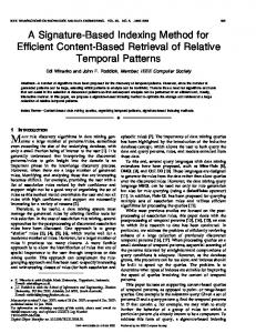
2094
IEEE TRANSACTIONS ON COMPUTERS, VOL. 63, NO. 8, AUGUST 2014
An Efficient Multiple Cell Upsets Tolerant Content-Addressable Memory Syed Mohsin Abbas, Soonyoung Lee, Sanghyeon Baeg, and Sungju Park, Member, IEEE Abstract—Multiple cell upsets (MCUs) become more and more problematic as the size of technology reaches or goes below 65 nm. The percentage of MCUs is reported significantly larger than that of single cell upsets (SCUs) in 20 nm technology. In SRAM and DRAM, MCUs are tackled by incorporating single-error correcting double-error detecting (SEC-DED) code and interleaved data columns. However, in content-addressable memory (CAM), column interleaving is not practically possible. A novel error correction code (ECC) scheme is proposed in this paper that will cater for ever-increasing MCUs. This work demonstrated that m parity bits are sufficient to cater for up to m-bit MCUs, with an understanding of the physical grouping of MCUs. The results showed that the proposed scheme requires 85% fewer parity bits compared to traditional Hamming distance based schemes. Index Terms—Error correcting code, multiple cell upsets, soft-error rate, singleerror correcting codes, parity bits, MCU confinement
1 INTRODUCTION CONTENT-ADDRESSABLE memory (CAM) is typically used for routing and policing in network routers and associating instructions in cache memories [1]. Due to disturbances from high-energy neutron particles, semiconductor memories are susceptible to soft errors [2]. Soft errors can be classified as single cell upsets (SCUs) or multiple cell upsets (MCUs). Baeg et al. observed MCU trends in 45-nm, 65-nm and 90-nm technologies [3]. Their observations clearly show that as technology is scaled down, MCUs become more and more problematic. Ibe et al. [4] simulated neutron-induced soft errors in SRAMs from a 250 nm to a 20 nm process; the results showed that the soft-error rate in SRAM increases by a factor of six to seven between 130 nm and 22 nm processes. The ratio of MCU to SCU increases by as much as 46% as the process technology node shrinks from 250 nm to 22 nm [4]. The interleaving approach has been used in memory devices to convert physical MCUs into logical SCUs; single-error correcting (SEC) codes can then be used to correct the logical SCUs. However, the interleaving approach is not practically possible for CAM due to the tight coupling of the hardware structures from both cells and comparison circuit structures [5]. Hamming distance based error correction code (ECC) schemes are usually applied to CAM in order to protect data against SCUs and MCUs [6], [9]. However, these Hamming distance based schemes require greater overheads in terms of parity bits, and typically provide protection for up to one or two bit upsets. Single-error correcting doubleerror detecting (SEC-DED) codes are the most commonly used for CAM; however, they can only correct 1-bit errors and can only • S.M. Abbas and S. Park are with the Computer Science and Engineering Department, Hanyang University, Ansan 426-791, Korea. E-mail:
[email protected],
[email protected]. • S. Lee and S. Baeg are with the Electronics and Communication Engineering Department, Hanyang University, Ansan 426-791, Korea. E-mail:
[email protected],
[email protected]. Manuscript received 08 Aug. 2012; revised 10 Jan. 2013; accepted 03 Apr. 2013. Date of publication 10 Apr. 2013; date of current version 15 July 2014. Recommended for acceptance by S. Shukla. For information on obtaining reprints of this article, please send e-mail to:
[email protected], and reference the Digital Object Identifier below. Digital Object Identifier no. 10.1109/TC.2013.90
detect double-bit errors. The mitigation of MCUs requires a large number of additional parity bits. Therefore, an alternate scheme, which can mitigate MCUs at a lower cost in terms of parity bits, is required. H.-J. Lee [7] proposed a new CAM cell architecture, in which each word in CAM is associated with a parity computing logic for immediate detection of bit flips. Soft errors are detected on the cost of addition of parity computing logic in each CAM word. Noda et al. [8] proposed using embedded DRAM (eDRAM) along with ternary content-addressable memory (TCAM) in order to mitigate SCUs and MCUs. In this approach, data entries are stored in both eDRAM and TCAM redundantly and a Hamming code ECC decoder/encoder is implemented at the interface between eDRAM and TCAM. In order to mitigate MCUs, during the refresh period of eDRAM, data are checked using ECC circuitry and corrected data are overwritten into the TCAM. One drawback of this approach is that it has redundancy and area overheads along with complex timing constraints. Dutta et al. [9] proposed an ECC methodology for the correction of adjacent double-bit errors. Their method is an extension of SEC-DED codes and uses the same number of bits as SEC-DED codes. Their proposed code can diagnose adjacent double-bit errors, but in real cases more than two errors are observed [4]. For SRAMs with 90 nm process technology, more MCUs than SCUs have been observed [10]. In short, to the best of our knowledge, previous works have primarily targeted SCU-related issues with a limited handling of MCUs; no simple and efficient technique exists for the mitigation of MCUs in CAM. In addition to single-bit parity encoding scheme, CAM duplication for SCU [11] and counting Bloom filter for MCU [12] have been suggested to recover from the soft errors. Parity bits for the interleaved words are similarly adopted to compensate false positives of the counting Bloom filter without changing internal structure of the CAM itself. However the interleaving scheme in CAM with global hardware overhead can be a burden. The preliminary version of this paper has discussed about the parity based code words to attack the MCU problem in CAM [13]. In this research, a novel ECC scheme is proposed by confining MCUs within a segment and using only a parity bit. After building code words comprising of both data and parity bits, new match criteria in a CAM is introduced without relying on any interleaving technique. Our scheme requires 85% fewer parity bits compared to previous Hamming distance based schemes. The rest of the paper is organized as follows. Section 2 briefly describes CAM architecture and experiment performed in Svedberg laboratory (TSL). The proposed ECC scheme is presented in section 3. The results and discussion are presented in section 4, and the conclusions in section 5.
2 PIPELINED CAM ARCHUTECTURE AND MCU CONFINEMENT In pipelined CAM architecture, a match-line is divided into multiple segments [14]. Each segment can evaluate the match result independently from the other segments, as shown in Fig. 1. This work develops a new error-correction scheme with two fundamental observations: MCU is confined in a segment with the aid of substrate and design engineering, and the pipelined CAM architecture can be used to independently process a segment. With the moderate efforts from substrate and design engineering practices, MCU can be confined within a segment such as the bits between well-tapping.
2.1
Experimental Observation
An observation was performed in Svedberg laboratory (TSL) for validation of MCU confinement assumption.
0018-9340 © 2013 IEEE. Translations and content mining are permitted for academic research only. Personal use is also permitted, but republication/redistribution requires IEEE permission. See http://www.ieee.org/publications_standards/publications/rights/index.html for more information.
IEEE TRANSACTIONS ON COMPUTERS, VOL. 63, NO. 8, AUGUST 2014
2095
Fig. 1. Pipeline CAM architecture: the pipeline is divided into multiple segments, each segment storing a fixed number of data bits. Fig. 3. Pipeline distribution of number of upsets in memory rows.
Fig. 4. A parity bit is generated for each group in a data word: , , and parity bits for the first, second, and third groups of a data word respectively.
are
Fig. 2. Parasitic p-well resistance between cells.
3 PROPOSED ERROR-CORRECTION SCHEME 2.1.1
Multiple Cell Upsets Between Well-Taps:
The well region and contacts are shared among multiple memory cells to increase area efficiency. A series of NMOSs of memory cells is fabricated in a p-well region, and p+ regions are implanted for building well-taps. The MCU characterizations between the well-taps were reported in [15]–[18]. Storage element of CAM cell is basically same as SRAM cell, so the parasitic bipolar effect of SRAM as reported in [15], [18] is also occurred in CAM structure. The parasitic bipolar effect induces the multiple errors of adjoining cells between the welltaps. Fig. 2 shows the parasitic p-well resistance (RP) between the cells. Each node of Fig. 2 means body bias of the cell. Well-taps are biased with GND, which is 0 V, and the body bias of both sides of the welltap is stabilized for the potential disturbance. Therefore, the bipolar action failure does not go over the well-tap, so upsets of MCU are located between the nearest well-taps [15], [18]. For example, the upsets of the Cell 0 and the Cell 4 are hardly occurred by bipolar actions.
2.1.2
Observation Results of Neutron-Induced Multiple Cell Upsetsd
Since a typical CAM cell consists of a few SRAM cells, neutroninduced MCU characterization has been performed on a 55 nm SRAM device. The SRAM consist of 72 banks and each bank has blocks. Each block has 512 rows and 256 columns. The SRAM block has well-taps of horizontal direction between 32 rows. The vendor name and more detailed architecture of the SRAM have been omitted for confidentiality. In order to induce soft errors, the SRAM devices were exposed to spectrum of white beams up to 180 MeV at the Svedberg laboratory (TSL). The tests were performed with various supply voltages, test patterns, and temperatures. The test patterns used were all zero, all one, and checkerboard patterns. The nominal supply voltage varied from to . The temperatures used were room temperature and 125 . The Failure in Time (FIT) per mega-bit (Mbit) was 267.38, and the occurrence ratio of MCUs in total events was 0.1. Fig. 3 shows the distribution of number of MCU upsets between well-taps. The number of upsets on the side of the well-tap has lower than others because the parasitic bipolar effects are inhibited as shown in Fig. 2. The experiment result is consistent with [16], [17]. The total number of collected MCUs was 2701, and the upsets of the 27-MCUs went across the well-taps. Therefore, occurring MCUs across the well-tap is 0.27 FIT per Mbit. The FIT value of the MCUs across the well-tap is small enough to be neglected in design process.
In the proposed coding scheme, data bits are divided into groups and a parity bit is calculated for each group, which make parity bits. The data bits are then placed at data segments in the way that no two bits from a group belong to the same segment and each segment contains data bits. All parity bits are placed in the parity-bit segment. A theorem is developed for generating parity bits; the theorem is based on the fact that one parity bit can detect single-bit errors in a data group. is the number of bits in a data word and is the size of the MCU. bits of data are divided into groups and is the number of bits in each group.
Theorem. One parity bit is generated to detect a single-bit error in a k-bit data group. The m parity bits from m data groups can detect up to m-bit MCU errors in a segment, where < .
Proof. Let
bits of data be divided into groups, each group having bits such that . Then a parity bit is independently calculated for each group. Let be the parity bit for the first group, for the second group and is the parity bit for the last th group; as a result, there are groups of data and parity bits. If only one bit changes from any group, then from the corresponding parity bit we can detect this 1-bit error. ◽
The bits in groups are assigned to S physical segments in a word such that only one bit from groups is exclusively mapped to one segment. For example, the first bits from groups are mapped to the first segment; this concept is similar to interleaving technique in memory design, and each segment contains data bits. All parity bits are placed in the parity-bit segment. Since each segment contains a bit from groups, an MCU in a segment will be translated as 1-bit error in groups; the parity bits can detect the single-bit error by definition. Therefore, parity bits are sufficient to detect any MCU as long as the MCU is contained within a segment of bits. Suppose that 15 bits of a data word are divided into three groups of five bits each, so that , , . The first group, is composed of five data bits, as shown in Fig. 4. Similarly the second group, is composed of and the third, is composed of . Parity bits are calculated for each group. is the parity of the first group, is the parity of the second group and is the parity of the third group, as shown in Fig. 4. If only one bit erroneously changes from any group, then its corresponding parity bit will detect this 1-bit error. Now we have CAM with S ( ) data segments and one paritybit segment. The data bits are then placed at data segments in such a
2096
IEEE TRANSACTIONS ON COMPUTERS, VOL. 63, NO. 8, AUGUST 2014
TABLE 1 Data Bits Are Stored in CAM with a Word Length of Six. Each Word is Divided into Three Segments, with Two Bits in Each Segment Fig. 5. Data bits are placed on data segments such that each segment contains bits from different groups and parity bits are placed in parity-bit segment.
way that no two bits from a group belong to one segment and each segment contains ( ) data bits as shown in Fig. 5. If an MCU occurs and it is limited to one segment only, with the help of corresponding parity bits, the MCU will always be detected. This is because, in a segment, each bit is from different group .
Lemma 1. Each valid code word including a parity segment differs from other code word by at least two segments.
Proof. Since each code word must be uniquely distinguished from other code word, any code word differs from other at least one segment. Consider the code words which differ only one segment from other. It can be easily seen that the parity segments must be different because only one segment of the code words differ from each other. In Table 1, it can be examined that all code words with three segments differ at least two segments. ◽ As the lemma states, due to parity bits, each valid code word differs from other code word by at least two segments. During the search operation, the search key is compared with all of the code words stored in the CAM. The search key is also a code word having data bits concatenated with parity bits.
Lemma 2. With confined segment based CAM with parity bits, any data word with a SCU can always be recognized as a match. Furthermore any data word with MCU whose size is no more than the size of a segment will always be correctly recognized as a hit.
Proof. All of the groups of the search key are compared with all of the segments of a stored code word. If more than one segment is a mismatch, then the search key is considered to be mismatched with the stored code word; otherwise, it is considered as a match. In other words, if the search key and the stored code word differ from one another by only one segment, this difference can be considered to be originated from soft errors and the search can be declared to be successful. When more than one segment of the search key and the stored code words do not match, it is declared to be a mismatch. Since a data word with either a SCU or MCU confined within a segment differs only one segment from the search key, this faulty data word is always considered as a match. ◽ For example, the data stored in CAM are depicted in Table 1, comprising four bits of data and two parity bits. This 6-bit code word is divided into two data segments and one parity-bit segments, as shown in Table 1. Suppose that a neutron hits and the fourth code word 001111 is changed to 000011; it is considered a two-bit MCU. When the search key 001111 is applied across CAM, the fourth code word differs from the search key by just one segment; all of the other stored entries differ by at least two segments. As long as only one segment is corrupted, it is considered as a match. In this way, bit MCU can be tolerated adding only parity bits.
4 RESULT AND DISCUSSION The proposed ECC scheme has been compared with previous Hamming distance based schemes [6], [9]. For the creation of Hamming distance between code words, BCH encoding is used, and the required number of parity bits is calculated. The parity bits required for Hamming distance based schemes were then compared with the parity bits required for our proposed ECC scheme. For any integer and there exists a primitive BCH code with the following properties [19].
. Block length: Parity check bits: . Minimum distance: . This code can correct or fewer errors over a span of bits. For CAM, , and so minimal block length becomes 127 bits. Therefore a truncated BCH code set is used for calculating parity bits, as used by Cheng et al. [20] for their W-ATM protocol design. A particularly popular SEC-DED (72, 64) code is a truncated (127, 120) Hamming code [21]. Table 2 shows the calculation of parity bits for different MCU sizes; the last column shows the truncated BCH codes. The parity bits required for Hamming distance based schemes are then compared with the parity bits required for our proposed ECC scheme, as shown in Fig. 6. The X-axis shows the size of MCU to be mitigated, and the Y-axis shows the parity bits required. Long gray bars show the number of bits required by Hamming distance based schemes and short black bars show parity bits required by our schemes. For example, if a 5-bit MCU is to be tolerated, then according to Hamming distance based schemes a Hamming distance of 11 is needed between code words. In order to create a Hamming distance of 11 between code words, 35 parity bits are needed for the truncated BCH code (72, 36), if the word length is assumed to be 72 bits for CAM. On the other hand, by using the proposed ECC scheme, only five parity bits are needed to mitigate a 5-bit MCU, provided the MCU is confined to a segment of five bits in size. By applying the proposed ECC scheme, the number of parity bits required is reduced up to a maximum of 85% as shown in the example case. This saving of parity bits comes from the assumption that the MCU is confined in one segment. Based upon this assumption, the number of parity bits required for MCU mitigation is equal to the segment size. Unlike the interleaving method, the proposed method is not changing the architecture of the memory. The implementation of parity tree requires only a few exclusive-or gates. Also the key matching technique proposed simply checks the segment distance among the search key and data code words. The power consumption TABLE 2 Calculation of Parity Bits Using a Truncated BCH Coding Scheme
IEEE TRANSACTIONS ON COMPUTERS, VOL. 63, NO. 8, AUGUST 2014
2097
Fig. 6. Parity overhead comparison (X-axis shows the MCU size to be mitigated and Y-axis shows parity bits required.).
Fig. 7. Comparison of the number of segments required for a particular segment size (X-axis shows the segment size and Y-axis shows the number of segments required).
of TCAM is generally referred to as E J/bit/search. An example of E is 6.57fJ in 0.18um technology [22]. Since proposed parity based key matching method and conventional CAM architecture are very similar, therefore no significant area, delay and power penalties will be observed. In the application of the proposed ECC scheme, a trade-off exists between the segment size and the number of segments. Segment size is directly related to MCU size; the greater the segment size, the greater the size of MCU which can be tolerated. On the other hand, the number of segments is inversely proportional to segment size. Fig. 7 shows the relationship between segment size and the number of segments. The gray line shows the number of segments and the black line shows segments size; as we can see, with the increase in segment size, the no. of segments required is decreased. For example, if we have CAM, and each segment is nine bits, then we require eight segments along one word line and we are able to mitigate MCU of up to eight bits.
entry 111111 just by one segment. Hence these two code words are termed as false positives for this particular corrupted CAM entry. For a particular CAM entry 001111, corrupted by MCU, there are only 2 possible false positive code words out of all possible code words. We can infer that for any particular CAM entry corrupted by MCU; there can be a maximum of false positive, where N is number of segments in code word. For the example presented above, as 6-bit code word is divided into 3 segments. False positive probability can be calculated by using the formula:
5 FALSE POSITIVE ANALYSIS False positive (or hit) indicates that due to a fault segment although the search key is not matched to any code word but considered as matched. Similarly false miss tells that due to MCU on a segment, matched code word is considered as not matched one. MCUs corrupting the data in CAM either result in a false hit or a false miss during search operation. In our scheme, by detecting a fault segment with MCU, faulty code words as well as fault free code words can be considered as matched ones. Therefore, there is no case where fault free code words are considered as a missed one, in other words, any false miss is not concluded in our scheme. Instead sometimes actually not matched one can be considered as a matched one, that is, false positive can occur in our scheme. In this section we will analyze false hits with the help of a simple example presented in section 3. Suppose we have 6-bit codeword having 4 bits of data and 2 parity bits. 6-bit codeword is divided into 3 segments; each segment contains only 2 bits. Since there are 4 bits of data, so all possible code words can be . All of these possible code words are listed in Table 1. Due to parity bits, each code word differs from other code word by more than one segment. Let the code word stored in CAM be 001111. A neutron hits and causes a 2 bit MCU in first segment and now code word becomes 111111. When the search key 001111 is applied, it differs from the corrupted code word just by one segment and differs from all other valid code words by more than one segment. This one segment difference, between search key and corrupted CAM entry, is ignored and search is declared as successful. However if code words like 110011 or 111100 are applied as search key, they will also be detected as match because both of these code words differ from the corrupted
Using eq. (1), false positive probability has been calculated for CAM. As shown in Fig. 8; false positive probability has been calculated for different segment sizes. For example if segment size is 8 bits then number of segments will be 9 comprising 8 segments for data bits and one segment for parity bits. The total number of data bits will be 64 and sample space of all possible code words will be then false positive probability can be calculated as
Fig. 8 show that as segment size increases false positive probability also increases, however it can be noted that the probability is extremely low. By having more well-taps for a data word, hence by decreasing segment size, less false positive can be achievable, but it will require more silicon area. As long as MCU is confined in one segment, application of proposed ECC can guarantee elimination of false miss. In case of MCU crossing boundary of a segment, false positive probability remains same as depicted in Fig. 8. However if MCU cross the boundary of a segment, false miss cases might occur, but as stated in section 2, the MCUs across the well-tap is small enough to be neglected in design process.
6 CONCLUSION In this work, a novel ECC scheme has been proposed to cater for the ever-increasing MCU problem in CAM. The parity bits required by previous Hamming distance based schemes were compared with the parity bits required by the proposed ECC scheme. The application of the proposed ECC scheme resulted in a saving of 85% of the parity bits required. This saving of parity bits came from the assumption that the MCU would be confined to one segment due to best practices applied in substrate and design engineering. This scheme resulted in
2098
[17] G. Gasiot, D. Giot, and P. Roche, “Multiple cell upsets as the key contribution to the total SER of 65 nm CMOS SRAMs and its dependence on well engineering,” IEEE Trans. Nucl. Sci., vol. 514, no. 6, pp. 2468–2473, Dec. 2007. [18] K. Yamaguchi, Y. Takemura, and Y. Saito, “Bipolar-mode multibit soft-error-mechanism analysis of SRAMs by three-dimensional device simulation,” IEEE Trans. Electron Devices, vol. 514, no. 11, pp. 3007–3017, Nov. 2007. [19] R.Togneri and C. deSilva, “Fundamentals of information theory and coding design,’ London, U.K.: Chapman & Hall, 2002, p. TdS02. [20] F. Cheng and J. M. Holtzman, “Wireless intelligent ATM network and protocol design for future personal communication systems,” IEEE Trans. Sel. Areas Commun., vol. 15, no. 7, pp. 1289–1307, 1997. [21] A. Molisch, “Channel coding and information theory’ in Wireless Commun., 1st ed. Wiley-IEEE Press, 2011, pp. 277–317 [22] S. Baeg, “Low-power ternary content-addressable memory design using a segmented match line,” IEEE Trans. Circuits Syst. I, Reg. Papers, vol. 55, no. 6, pp. 1485–1494, Jul. 2008.
For more information on this or any other computing topic, please visit our Digital Library at www.computer.org/publications/dlib.
▽
Fig. 8. False positive probability over different segment sizes (X-axis shows false positive probability and Y-axis shows the segment size in number of bits).
IEEE TRANSACTIONS ON COMPUTERS, VOL. 63, NO. 8, AUGUST 2014
a trade-off in terms of calculating segment size and the number of segments, and this trade-off and false positive probability was also estimated in this research work.
ACKNOWLEDGMENT This research was supported in part by the “GRRC” Project of Gyeonggi Provincial Government, Republic of Korea and the National Research Foundation of Korea (NRF) Grant (MEST) (20100026822).
REFERENCES [1] K. Pagiamtzis and A. Sheikholeslami, “Content-addressable memory (CAM) circuits and architectures: A tutorial and survey,” IEEE Trans. Solid-State Circuits, vol. 41, no. 3, 2003, pp. 712–727. [2] S. Baeg, P. Reviriego, J. A. Maestro, S.Wen, and R. Wong, “Analysis of a Multiple Cell Upset Failure Model for Memories,’ in IEEE Workshop on Silicon Errors in Logic-System Effects (SELSE), Mar. 2009 [Online]. Available: http:// softerrors.info/selse/images/selse_2009/Papers/selse5_submission_7.pdf [3] S. Baeg, S. Wen, and R. Wong, “SRAM interleaving distance selection with a soft error failure model,” IEEE Trans. Nucl. Sci., vol. 56, no. 4, pp. 2111–2118, Aug. 2009. [4] E. Ibe, H. Taniguchi, Y. Yahagi, K. Shimbo, and T. Toba, “Impact of scaling on neutron induced soft error in SRAMs from an 250 nm to a 22 nm design rule,” IEEE Trans. Electron Devices, vol. 57, no. 7, pp. 1527–1538, Jul. 2010. [5] S. Baeg, S. Wen, and R. Wong, “Minimizing soft errors in TCAM devices: A probabilistic approach to determining scrubbing intervals,” IEEE Trans. Circuits Syst., Reg. papers, vol. 57, no. 4, pp. 814–822, Apr. 2010. [6] K. Pagiamtzis, N. Azizi, and F. N. Najm, “A soft-error tolerant contentaddressable memory (CAM) using an error-correcting-match scheme,” in Proc. IEEE Custom Integr. Circuits Conf. (CICC‘06), 2006 pp. 301–304. [7] H.-J. Lee, “Immediate soft error detection using pass gate logic for content addressable memory,” Electron. Lett., vol. 44, no. 4, pp. 269–270, Feb. 2008. [8] H. Noda, K. Dosaka, F. Morishita, and K. Arimoto, “A soft-error-immune maintenance-free TCAM architecture with associated embedded DRAM,” in Proc. IEEE Custom Integr. Circuits Conf., 2005 pp. 451–454. [9] A. Dutta and N. A. Touba, “Multiple bit upset tolerant memory using a selective cycle avoidance based SEC-DED-DAEC Code,” in Proc. 25th IEEE VLSI Test Symp., May 2007, pp. 349–354. [10] R. K. Lawrence and A. T. Kelly, “Single event effect induced multiple-cell upsets in a commercial 90 nm CMOS digital technology,” IEEE Trans. Nucl. Sci., vol. 55, no. 6, Oct. 2008, pp. 3367–3374. [11] S. Pontarelli, M. Ottavi, and A. Salsano, “Error detection and correction in content addressable memories,” in IEEE Int. Symp. Defect and Fault Tolerance in VLSI Syst. (DFT), 2010, pp. 420–428, doi: 10.1109/DFT.2010.56. [12] S. Pontarelli and M. Ottavi, “Error detection and correction in content addressable memories by using bloom filters,” IEEE Trans. Comput., doi: 10.1109/TC.2012.56. [13] S. M. Abbas, S. Baeg, and S. Park, “Multiple cell upsets tolerant contentaddressable memory,” in Proc. IEEE Int. Rel. Phys. Symp., Apr. 2011, pp. 863–867. [14] K. Pagiamtzis and A. Sheikholeslami, “Pipelined match-lines and hierarchical search-lines content-addressable memories,” in Proc. IEEE Custom Integr. Circuits Conf., 2003, pp. 383–386. [15] K. Osada, K. Yamaguchi, Y. Saitoh, and T. Kawahara, “SRAM immunity to cosmic-ray-induced multi errors based on analysis of an induced parasitic bipolar effect,” IEEE J. Solid-State Circuits, vol. 139, no. 5, pp. 827–833, May 2004. [16] D. Radaelli, H. Puchner, K. Wong, and S. Daniel, “Investigation of multi-bit upsets in a 150 nm technology SRAM device,” IEEE Nucl., vol. 512, no. 6, pp. 2433–2437, Dec. 2005.