15.3
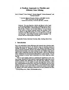
An Efficient Scalable and Flexible Data Transfer Architecture for Multiprocessor SoC with Massive Distributed Memory Sang-Il Han*,**, Amer Baghdadi***, Marius Bonaciu**, Soo-Ik Chae*, Ahmed. A. Jerraya** *Department of Electrical Engineering, Seoul National Univ., Seoul, Korea
**SLS Group, TIMA Laboratory, Grenoble, France
***Electronics Department, ENST Bretagne, Brest, France
{sihan,chae}@sdgroup.snu.ac.kr
{marius.bonaciu,ahmed.jerraya}@imag.fr
[email protected]
constraint that such architectures should deal with is to handle high data transfer rates encountered in emerging complex applications. The data transfer architecture should be scalable to handle applications of varying complexity requiring a different number of processors, different bandwidth and/or different latency. The busbased MPSoC fails to scale well because it employs global order of data transfer defined by central arbitration and the limited number of data transfer. In order to overcome this issue, we adopt two assumptions: 1) the read and write operations of a data transfer should be decoupled, and 2) the data transfer engines should be distributed to allow massive data transfers concurrently. These two assumptions have already been employed in classical massively parallel processors architectures [2] and the work presented here adapts this concept to multiprocessor SoC with massively distributed memory. The key contribution is to allow customization of the communication infrastructure. The data transfer architecture should also be flexible to enable designs of different configurations in order to (1) fit the precise application needs for low-cost implementation and (2) adapt different kinds of computation and memory subsystems. This flexible data transfer architecture can be built using a componentbased design methodology [3][4]. This paper proposes an efficient scalable and flexible data transfer architecture for MPSoC with massive distributed memory. The architecture is organized as Distributed Memory Server (DMS) that consists of high-performance and flexible memory service access points (MSAPs), data network, and control network. The MSAP acts as Network Interface and Data Transfer Engine. Synthesis results show that a typical MSAP provides efficient results in terms of size and throughput. The scalability of the proposed DMS will be illustrated through two implementations of an MPEG4 video encoder. The experiments show clearly how the DMS can be adapted to accommodate different multiprocessor SoC configurations requiring different data transfer bandwidths. The rest of the paper is organized as follows. Section 2 presents state of the art on data transfer architectures. Section 3 presents the scalable data transfer architecture (i.e. DMS) model. Section 4 details the high-performance and flexible memory service access point (MSAP). Section 5 presents several experiments to analyze the efficiency of the proposed DMS. Finally, section 6 gives our conclusions on the work presented in this paper.
ABSTRACT Massive data transfer encountered in emerging multimedia embedded applications requires architecture allowing both highly distributed memory structure and multiprocessor computation to be handled. The key issue that needs to be solved is then how to manage data transfers between large numbers of distributed memories. To overcome this issue, our paper proposes a scalable Distributed Memory Server (DMS) for multiprocessor SoC (MPSoC). The proposed DMS is composed of: (1) highperformance and flexible memory service access points (MSAPs), which execute data transfers without intervention of the processing elements, (2) data network, and (3) control network. It can handle direct massive data transfer between the distributed memories of an MPSoC. The scalability and flexibility of the proposed DMS are illustrated through the implementation of an MPEG4 video encoder for QCIF and CIF formats. The experiments show clearly how DMS can be adapted to accommodate different SoC configurations requiring various data transfer bandwidths. Synthesis results show that bandwidth can scale up to 28.8 GB/sec.
Categories
and Subject Descriptors: B.4.3 [Input/Output and Data Communications]: Interconnections (Subsystems); B.8 [Hardware]: Performance and Reliability General Terms: Design, Performance, Experimentation. Keywords: Multiprocessor SoC, Message passing, Data transfer architecture, Memory Server, Network on chip, Network Interface. 1. Introduction Current multimedia and telecommunication applications require complex high-performance multiprocessor SoC (MPSoC). Raising communication abstraction level and decoupling communication from computation have been proposed as the solution to master the design complexity of MPSoC [1]. To that end, high level programming models, such as message passing [17][18], are quite appropriate. However, to achieve the required high-performance, more and more efficient architectures able to handle message passing programming models are still required. The main Permission to make digital or hard copies of all or part of this work for personal or classroom use is granted without fee provided that copies are not made or distributed for profit or commercial advantage and that copies bear this notice and the full citation on the first page. To copy otherwise, or republish, to post on servers or to redistribute to lists, requires prior specific permission and/or a fee. DAC 2004, June 7–11, 2004, San Diego, California, USA Copyright 2004 ACM 1-58113-828-8/04/0006…$5.00.
2. Related work on data transfer architecture Massive data transfer architectures are well handled in the classical massively parallel processors systems. Machines [2] like nCUBE, CM-5, Intel Paragon, and Meiko CS-2 include sophisticated mechanism for direct data transfer between distributed memories. These architectures are generally scalable
250
allows data transfer from its local memories to other subsystems and from other subsystems to its local memories. Data transfers are requested by subsystems using the control network. MSAP delivers transaction requests ordered by its subsystem and synchronization information via control network. It also executes data transfer between its local memory and other subsystem’s memory via data network. The proposed DMS allows: 1) Decoupling of read and write operations: MSAP receives a data transfer request from the attached PE and splits it into local request (read or write) and remote request (write or read). Then, it sends the remote requests to the target MSAPs via the control network. 2) Distributing execution requests: the distributed MSAPs execute the memory-to-memory data transfers ordered by a distributed scheduler (each MSAP includes an independent local scheduler). The proposed DMS decouples computation from communication through the MSAP and allows parallel execution of computation and communication through the processing power of MSAP. In this paper, we use an AMBA bus for the control network and a partial point to point interconnect for data network. The proposed DMS has no assumption about control network and data network. MSAP can accommodate any type and any combination of control and data networks, e.g. bus, full point-to-point link, packet switch, and circuit switch. The structure of the networks themselves is out of the scope of this paper. We will discuss only the connection between the networks and the MSAPs.
and support performance-efficient data transfers between large numbers of memories. However, all of them lack flexibility and have little concern about resource constraints. So these architectures are not suitable for data transfer in SoC that should satisfy severe performance, area, power, and cost constraints. These constraints can be achieved only when the communication structure can be customized to each specific application. Conventional DMA engines [5] support efficient data transfers, but they can execute only sequential data transfer. Multiple DMA engines used in classical multiprocessor system enable the execution of multiple concurrent data transfers, however such a solution will not be cost-effective because the architecture is not flexible. This will be shown in section 5. The DMA engines in [6][7] support performance-efficient and concurrent data transfers. But the scalability of data transfers is limited by the use of a unique global arbiter. Several on-chip network [10][11] and network interfaces [8][9] handle data transfers between distributed memories on a chip. These interfaces support scalable data transfers. The main restriction of existing NoC solutions is the restrictions of the number of channels used to link computation or memory nodes to the network. This generally introduces congestion in the nodes using the network. A typical case is a slow computation node inducing saturation of the shortage capacity of the network and then blocking all data transfers in the network. In order to avoid that, highly flexible access to the network is required. Additionally, several academic and industrial research projects proposed high performance architectures for massive data transfer applications. Among those we can cite Philips Nexperia™ DVP [12], and TI OMAP™ [13]. Even if their architectures are highly programmable, they lack scalability. The key contribution of this paper is to provide both scalable and flexible architecture allowing the specific needs of each application to be accommodated. It combines the scalability of NoC solutions with flexibility of component-based design to customize the data transfer architecture.
4. Memory Server Access Point A Memory Server Access Point (MSAP) acts as a Network Interface that provides the link between NoC and subsystems (Figure 1). It also acts as a data transfer engine that transfers data between the attached memory and other memories of other MSAPs. Figure 2 shows global structure of an MSAP. It is composed of 5 basic functions:
3. The Distributed Memory Server
Subsystem 0
Subsystem k
Local Bus 0
Local Bus k
m
P
MSAP
… …
m
IP
MSAP
… …
M MSAP
…
Local memory
P
Processor
M
Global memory
IP
IP
MSAP Memory Service Access Point
Control Network
2)
Data
Data Network
Local Request Acceptor
Wrapper
Memory Scheduler
PE
Figure 2. Basic functions of the MSAP 1)
…
Remote Request Acceptor
mem
Subsystem
Subsystem n m
Memory Activator
Wrapper
Control Network
Wrapper
Data Network
Wrapper
MSAP
Distributed memory server (DMS) acts as a server that services subsystems by executing data transfers between their corresponding memories. Figure 1 shows a global view of an MPSoC architecture using DMS. The system is composed of computation subsystems, memory subsystems and a DMS. A computation subsystem is composed of one processing element (PE), local memory and local bus. A memory subsystem consists of one or more memories. All subsystems are connected to the DMS through Memory Service Access Points (MSAP).
3)
Control
DMS
4)
Figure 1. MPSoC with the DMS The DMS is composed of MSAPs, control network and data network. Each subsystem is connected to a specific MSAP that
251
Local Request Acceptor (LRA): It accepts data transfer requests from the attached PE and splits them into local requests and remote requests. It sends the remote requests to the target MSAPs via control network. (A data transfer is composed of local read (write) operations and remote write (read) operations.) Remote Request Acceptor (RRA): It receives the remote requests from other MSAPs. Memory Scheduler (MS): It schedules the received requests from LRA or RRA. Memory Activator (MA): It executes read (write) request selected by its memory scheduler.
5)
information for the data transfer, i.e. memory address, transfer size, transfer mode, port number, and block transfer mode. MSAP does not need an LRA if the attached subsystem is a memory subsystem or slave computation subsystem. Possible configurations of the LRA include interrupt generation, scatter/gathering (i.e. automatic link of data transfers), and block transfer (e.g. macro-blocks in video encoder). 4.1.2 Remote Request Acceptor The RRA is connected to the control network through a CNW in order to receive and handle the requests from LRAs. The RRA 1) receives connection setup/release and data transfer requests from other LRAs (including LRA of the same MSAP), 2) sends a TD in data transfer request to Memory Scheduler, and 3) makes acknowledgement of the received requests. The MSAP doesn’t need an RRA if the memory of the attached subsystem is not accessed by other LRAs. 4.1.3 Data Queue A Data queue between the Memory Activator and a Data Network Wrapper hides delay jitter for avoiding the unnecessary activations of the data network and memory. A data queue provides warning signal. The warning signal is set or cleared according to its five latency levels: not empty, 1/4 filled, 1/2 filled, 3/4 filled and not full. The Memory Scheduler uses the warning signal for avoiding unnecessary context switch. Possible configurations of a Data Queue include its size and latency level. In addition, the chain queue (CHAIN) shown in Figure 3 contains the next transfer descriptor for scatter/gathering feature mentioned in section 4.1.1. 4.1.4 Control Queue A control queue between the LRA (or RRA) and the control network hides the latency due to the contention of the control network. The possible configuration of a Control Queue concerns its size. In addition, the completion queue (DONE) shown in Figure 3 contains the descriptors of the completed data transfer. 4.1.5 Memory scheduler The Memory Scheduler contains a set of registers (called port context) describing the status of each data port. A port context consists of 6 registers as shown in Figure 4.
Wrappers: they adopt the MSAP to PE, memory, data network and control network.
The different parts can be customized and assembled using a flexible scheme to Accommodate different networks and heterogeneous subsystems thanks to wrappers. Accommodate different communication bandwidths and latency thanks to modular decomposition in separate basic functions. The flexibility and configuration of MSAP will be explained in the next section. Not all of the basic functions are required for all possible configurations.
4.1 MSAP architecture Figure 3 details the general architecture of the MSAP. Each component will be explained in the rest of this section. The MSAP is connected to the data network through data input/output ports. A data channel is established by linking a data input port and a data output port. The MSAP can transfer data to another MSAP through a data channel. For the control ports, control channels and the control network, we have exactly the same behavior. Each data port has a FIFO buffer that connects the Memory Activator (MA) to the data network. Each control port has two FIFO buffers: one connects Local Request Acceptor (LRA) to the control network and the other connects Remote Request Acceptor (RRA) to the control network. Note that RRA and LRA are separated in order to avoid unnecessary instantiation (flexibility). DNW
DNW
…
…
…
Data output ports
Ctrl Output port
Control Network
…
Ctrl input port
…
Data Network
…
Data input ports
Local memory
MW
MA DNW
READY
EXIT
DNW
MS
DONE
Local bus
DONE
CONN, COMM CHAIN
CNW NETID, DONE NETID, DONE
TD
RRA
TD
LRA
PW
Processor
CNW CONN, COMM
MSAP
Content
Offset
Figure 3. General detailed architecture of the MSAP
Local memory address (laddr)
0x0
The buffers can be operated by two clocks: 1) data or control network clock and 2) subsystem clock. The dotted lines on the buffers in Figure 3 shows three clock domains, i.e. data network clock domain, control network clock domain and subsystem clock domain. The separation of network clock domain from subsystem clock domain allows integrating subsystems with different clock frequency with DMS. 4.1.1 Local Request Acceptor LRA is connected to the PE of a subsystem through PE Wrapper (PW) in order to receive and handle the requests of the local subsystem. LRA 1) receives connection setup/release requests and data transfer requests from the attached PE, 2) reports the status of requests to the attached PE, 3) sends remote requests to the target RRAs via the control network, and 4) sends a Transfer Descriptor (TD), to the Memory Scheduler (MS). A TD contains the
Remote memory address (raddr)
0x4
Chain address (caddr)
0x8
Transfer configuration (ch_cfg)
0x10
Remote control network ID (rcnetid)
0x14
Remote data network ID (rdnetid)
0x18
Figure 4. Context registers of a data port Memory Scheduler 1) selects one of the port contexts according to its scheduling policy, 2) sends the selected context to the local Memory Activator, and 3) updates the port contexts according to the received TDs. Possible configurations of the MS include scheduling policy, priority, the size of ready queue and the number of MA. 4.1.6 Memory activator Memory Activator (MA) receives an active context from Memory Scheduler and executes it.
252
(6) The RRA parses the COMM request and sends the corresponding TD to its MS. (7) The MS schedules the received TD. (8),(9) The MA of the global memory transfers data from the global memory to the data queue according to the received TD. (10) The data (of the data queue of the global memory) is transferred to the data queue of the local memory via the data network. (11),(12) The MA of the local memory transfers the data from the data queue to the local memory according to the received TD. If the TD is about write operation, the memory scheduler sends DONE signal to the LRA and the RRA for synchronization after transfer completion.
MA 1) executes the data transfer by generating memory address, memory control signals and queue control signals according to the received context, 2) switches context when the data transfer is completed, a preemption condition is occurred, or the data queue is empty (read operation) or full (write operation). Figure 5 shows the detailed connections between the MA and the data input ports. Network clock Data Network
nEMPTY
Local clock
WEN
nEMPTY
nFULL
REN
DNW REN
…
…
Data input ports
WEN
nEMPTY
nEMPTY
DNW REN
MWEN
nEMPTY RDATA REN
Memory MA
MWDATA MREADY
or Local bus
CNW
MUX nFULL
P,m
MSAP2
REN
(5)
RRA
CNW
Figure 5. Data flow between a subsystem and the data network (4)
The MSAP can have several MAs for concurrent data transfers if the subsystem has several memories, e.g. scratch-pad memories [15][16]. So the possible configuration of the MA concerns the number of ports. 4.1.7 Wrappers An MSAP can be connected to four kinds of components: PE, memories, data network and control network. For flexible instantiation of MSAP, four kinds of wrapper are required, i.e. PE Wrapper (PW), Memory Wrapper (MW), Data Network Wrapper (DNW) and Control Network Wrapper respectively. A PW converts the protocol of LRA to the memory access protocol of PE. In the current version, the protocol of the LRA is the AMBA protocol. An MW provides the logical interface of memory to an MA. If the attached memory is a local memory and it is connected to a local bus, the memory wrapper converts the local bus protocol to the queue protocol or vice versa. If the memory is global, e.g. an embedded SRAM, an embedded flash memory, or an embedded DRAM, the MW is a physical memory controller [7]. DNW and CNW convert the queue protocol to the network protocol or vice versa. For example, if data network is packetswitch, DNW is packetsizer or de-packetizer.
(10) DNW
(2)
M
MA
(8)
(9)
(4)
(3)
(5) (6)
MSAP1 (11) (12)
(7)
m
MA
(8)
(3) CNW
COMM Network
CNW
DNW CNW RRA MS MA
(1)
MS
(7)
DNW
M MA MS LRA CNW DNW
(6)
(7)
MS
(1) (2) (a)
(9)
(10)
P
LRA
(11) (12)
MSAP1
Network
MSAP2
(b)
Figure 6. A data transfer example between two MSAPs In distributed memory architectures, data consistency is an important issue. DMS assumes that this issue is considered by a higher-level protocol. That means, if the DMS is used in a message-passing architecture, the message-passing protocol will solve this issue [19].
4.3 Flexible configuration of the MSAP The flexible architecture of the MSAP enables various configurations that allow to 1) integrate different networks and heterogeneous subsystems, 2) accommodate different communication bandwidths and latency, and 3) implement DMS at low-cost. MSAP is able to adapt various types of PEs, memories, control networks, and data networks to the DMS through the corresponding wrapper, i.e. PW, MW, CNW and DNW. Furthermore, it is able to integrate various clock domains of subsystems and networks through queues that are operated by two clock frequencies. To accommodate such various data transfers, MSAP allows the configuration of the number of MAs, the number of ports of each MA, the queue size of each port, the priority of each port, the latency level of each port, and the scheduling policy. Besides that, to customize the MSAP according to a specific functionality, the MSAP can be configured to include or not the following components: RRA, LRA (Interrupt generation, Block Transfer, and scatter/gathering). Finally, the automatic configuration and generation of the DMS is important to reduce the design time. A component-based design methodology could be a proper approach. We believe that the proposed architecture model for the DMS is already suitable for a systematic design. Automation is out of the scope of the work presented in this paper. Yet, it concerns our future work.
4.2 Data transfer Models Three procedures are required to transfer data between two MSAPs. 1) Connection setup: the two MSAPs open a channel by reserving two ports and exchange the data network IDs of these ports. 2) Data transfer: the two MSAPs transfer the data via the channel. 3) Connection release: the two MSAPs release the two ports of the channel. We assume that the control network ID of the target port is known before the connection setup. Figure 6 shows an example of a data transfer from a global memory to a local memory. The procedure of the data transfer is as follows. (1) The processor writes the data transfer information into its control registers. (see Figure 4) (2),(3),(4),(5) The LRA sends a command (COMM) request to the RRA of the global memory via the control network. It also sends a TD to the local MS.
253
5. Experiments Several experiments were conducted in order to verify the scalability and flexibility of DMS under the parameters and environment shown in Table 1.
Port number
MSAP w/o data queue
1 2 4 8 16
0.136 0.177 0.245 0.394 0.685
Data queue 0.026 0.052 0.103 0.207 0.413
Total area 0.161 0.229 0.349 0.600 1.099
Language
SystemC RTL description
Table 3. Areas (mm2) of an MSAP about port number
Technology
TSMC (slow) 0.18µm
Compiler
Synopsis Design Compiler
Control Network
AMBA bus
Data network
Point-to-point
Second, to verify the scalability and flexibility of DMS, we conducted two other experiments. One is the design of an MPEG4 [14] encoder that can encode QCIF image at 25 frames/sec by using 4 ARM7 processors. The other is the design of an MPEG4 encoder for CIF image by using 16 ARM7 processors.
Clock freq.
200 MHz
MPEG4 Encoder Q
Table 1. Parameters and environment of the experiments
Configuration
1 2 3 4 5 6 7
BASIC+RRA BASIC+LRA +RRA +INTR +BLOCK +CHAIN +TWO_PRIO
MSAP w/o data queue 0.129 0.200 0.235 0.240 0.245 0.321 0.348
Data queue
Total area
0.103 0.103 0.103 0.103 0.103 0.121 0.121
0.233 0.303 0.338 0.344 0.349 0.442 0.470
Fc
Px
Xth processor Cam Camera
M
Global Memory
ME
ZIG
Net
First, to evaluate the flexibility of MSAP, we have synthesized several MSAPs by using various configurations. Table 2 shows the area for each configuration. The basic configuration (BASIC) of an MSAP is the one with only MA, MS, CNW, DNW, Data queue and Control queue. The INTR, BLOCK, CHAIN, and TWO_PRIO represent a configuration with interrupt feature, block transfer feature, linked-list feature, and two priority feature of MSAP respectively. #
DCT
MC
VLC IQ
IDCT
Fn-1
Net
Network Device P3,P4
Cam Net
Cam
M
P1
P2
P2 P2
Fn
(b)
(a)
Figure 7. (a) Block diagram, (b) System-level architecture of an MPEG4 system for QCIF format Figure 7 (a) shows the Block diagram of an MPEG4 system. The MPEG4 encoder receives images from a camera, encodes the images and then sends the encoded bit-stream to network device, e.g. wireless LAN. Figure 7 (b) shows the system-level architecture of an MPEG4 system for QCIF format. Each node represents a subsystem and each edge represents an abstract channel. A camera writes a part of image from its buffer to the global memory. Each processor reads a part of image from the global memory and executes encoding algorithm (ME, MC, DCT, IDCT and so on). P1 makes a bit-stream from the results by executing VLC and sends it to network device. The structure of MPEG4 system for CIF format is hierarchical combination of MPEG4 system for QCIF format.
Table 2. Areas (mm2) of an MSAP for various configurations For all of these configurations, we fixed the number of data ports to 4 and we used a 2-port, 32bit wide and 16-word deep register file as data queue. In this case, the MSAP (with four data ports) has an aggregate bandwidth of 4×200MHz×4bytes = 3.2 GB/sec. However, in general case, the bandwidth of MSAP is limited by the memory bandwidth. This result shows how configuration may affect heavily the cost of MSAP.
Figure 8 shows the corresponding implementation as an MPSoC with the DMS architecture. Property # of MSAP # of port Area of DMS Area over DMAs+NIs Area over DMAs Aggregate bandwidth Latency of read transfer Latency of write transfer
The scalability of the number of data ports is also a key feature of MSAP. The synthesis results of several MSAPs with different numbers of ports are shown Table 3. For all of them, we used the configuration number 5 of Table 2. The MSAP compares favorably to classical DMA. The gate count (NAND2 equivalent) of a commercial DMA engine [5] (8 channels, 32bit*4 words data queue per each port, with scatter/gathering feature) is about 82k. The gate count of the proposed data transfer engine (8 channels, 32bit*8 words data queue per each port, with scatter/gathering feature) is about 68k, so it is about 20% smaller than the commercial DMA.
DMS for MPEG4 QCIF 7 18 1.61 mm2 45% 86% 7.2 GB/sec 10 6
DMS for MPEG4 CIF 22 72 5.93 mm2 41% 80% 28.8 GB/sec 10 6
Table 4. Experimental results of two DMS versions Table 4 summarizes the results obtained from the two DMS implementations. These results show clearly the bandwidth scalability and the area efficiency of the proposed DMS.
254
Local bus 1
Local bus 0 Net Ctrl
m
m
Cam Ctrl
Local bus 2 M
m
LRA
MA
MS
MA
MS
DNW
CNW
DNW
CNW
m
LRA
MA
MS
MA
MS
RRA
RRA
Local bus 3
P1
DNW DNW DNW DNW DNW CNW
DNW DNW DNW DNW DNW
Local bus 4 m
P2
MS
m
LRA
LRA
MA
Local bus 5
P3
MA
P4
LRA
MS
MA
MS
RRA
RRA
RRA
RRA
CNW
DNW DNW CNW
DNW DNW CNW
DNW DNW CNW
Control Network
Data Network
Figure 8. MPEG4 system for QCIF format using the DMS architecture [5] ARM PrimeCell™ DMA Controller, http://www.arm.com/armtech/PrimeCell?OpenDocument
6. Conclusion In this paper, we described a Distributed Memory Server (DMS) to handle massive data transfers between large numbers of distributed memories on MPSoC. It consists of high-performance and flexible Memory Service Access Points (MSAPs), data network and control network. The DMS provides 1) performanceefficient data transfer mechanism between subsystems of MPSoC, 2) a scalable solution to handle a large application field, and 3) flexible designs to integrate with heterogeneous subsystems at lowcost. An MSAP, which is the main component of the DMS, receives data transfer requests from the attached subsystem of an MPSoC, schedules them and then executes the received data transfer requests concurrently. Synthesis results of different configurations show clearly the flexibility of the proposed architecture of MSAP. Compared to a conventional DMA engine of similar functionality, an MSAP reduce the area by about 20%. A typical instance of MSAP runs at 200Mhz, occupies 0.349 mm2 in a 0.18 µm technology, and has an aggregate bandwidth that scales up to 3.2 GB/sec. The scalability and flexibility of the proposed DMS are illustrated through the implementation of an MPEG4 video encoder for QCIF and CIF formats. The experiments illustrate how DMS can be adapted to accommodate different SoC configuration requiring different data transfer bandwidths. The DMS for CIF requires 22 MSAPs and its aggregate bandwidth rises up to 28.8 GB/sec. Its area is 55%~59% smaller than the combination of conventional DMAs [5] and network interfaces [8].
[6] Dave Comisky et al, “A Scalable High-Performance DMA Architecture for DSP Applications,” in Proceedings of ICCD 2000. [7] MemMax™ Memory Scheduler, http://www.sonicsinc.com/sonics/products/memmax [8] A. Radulescu et al, "An Efficient On-Chip Network Interface Offering Guaranteed Services, Shared-Memory Abstraction, and Flexible Network Programming," in Proceedings of DATE'04. [9] P. Bhojwani et al. “Interfacing cores with on-chip packetswitched networks,” In IEEE Proc. On VLSI Design, 2003 [10] E. Rijpkema, et al., “Trade offs in the design of a router with both guaranteed and best-effort services for networks on chip,” in Proceedings of DATE'03. [11] William J. Dally and Brian Towles,“Route Packets, Not Wires: On-Chip Interconnection Networks,” in Proceedings of DAC'02. [12] Philips Nexperia™ DVP, http://www.semiconductors.philips.com/platforms/nexperia [13] TI OMAP™ Platform, http://www.ti.com/sc/docs/apps/omap/overview.htm [14] MPEG-4 Standard, http://www.chiariglione.org/mpeg/standards/mpeg-4/mpeg4.htm
7. REFERENCES
[15] Motorola DSP56311, http://www.motorola.com/brdata/PDFDB/docs/DSP56311.pdf
[1] K. Keutzer et al. “System-level design: Orthogonalization of concerns and platform-based design,” IEEE Trans. On CAD of Integrated Circuits and Systems.
[16] ARM ARM946E-S, http://www.arm.com/products/CPUs/ARM946ES.html
[2] Culler D. E. et al, “Parallel Computer Architecture, A Hardware/software approach,” Morgan Kaufmann Inc, San Francisco California, 1999, ISBN 1-55860-343-3.
[17] T. McMahon, A. Skjellum, “eMPI/eMPICH: Embedding MPI,” In Proceedings of the Second MPI Developer's Conference, University of Notre Dame, South Bend, IN, 1996, pp. 57-65. 22
[3] A. Baghdadi, D. Lyonnard, N.-E. Zergainoh, and A.A. Jerraya, “An Efficient Architecture Model for Systematic Design of Application-Specific Multiprocessor SoC,” in Proceedings of DATE'01.
[18] J. Kohout and A. George, "A High-Performance Communication Service for Parallel Computing on Distributed DSP Systems," Parallel Computing, Vol. 29, No. 7, July 2003, pp. 851-878.
[4] Jerraya et al., “Component-Based Design Approach for Multicore SoCs,” in Proceedings of DAC'02.
[19] Junyu Peng and Daniel Gajski. “Optimal Message-Passing for Data Coherency in Distributed Architecture,” in Proceedings of ISSS’02.
255