Jan Verspecht bvba Gertrudeveld 15 1840 Steenhuffel Belgium email:
[email protected] web: http://www.janverspecht.com
An improved coupling method for time domain load-pull measurements
Fabien De Groote, Jan Verspecht, Christos Tsironis, Denis Barataud, Jean-Pierre Teyssier
Conference Record of the 65th ARFTG Conference Long Beach, California, USA, June 2005
© 2005 IEEE. Personal use of this material is permitted. However, permission to reprint/republish this material for advertising or promotional purposes or for creating new collective works for resale or redistribution to servers or lists, or to reuse any copyrighted component of this work in other works must be obtained from the IEEE.
An improved coupling method for time domain Load-Pull measurements Fabien De Groote1, Jan Verspecht2, Christos Tsironis3, Denis Barataud1, Jean-Pierre Teyssier1 1
IRCOM-CNRS, University of Limoges,7 rue Jules Vallès 19100 Brive, France 2 Jan Verspecht bvba, Gertrudeveld 15, 1840 Steenhuffel, Belgium 3 Focus Microwaves, 1603 St. Regis, Dollard-des-Ormeaux, Quebec, Canada H9B 3H7
Abstract — This paper describes an efficient coupling method improving the non linear time domain large signal load-pull measurements of active devices. This approach consists in a small RF loop fixed near the blended line that takes place between the DUT and the tuner. We take benefit of two advantages : extremely low losses induced by the coupler, and measurements taken very close to the DUT plane. It is shown that this simple coupling solution offers an average directivity better than 15 dB (before calibration) along a wide RF band from 2 to 18 GHz. This solution is compared with the classical approach of a distributed coupler connected before and after the tuner. A LSNA calibration has been performed, it exhibits an average directivity better than 35 dB.
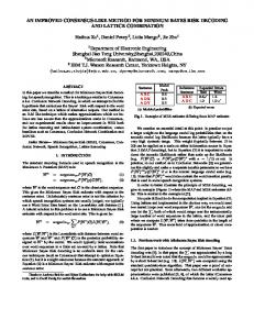
fields, particularly the phase opposition for the magnetic one with incident and reflected waves (Fig. 2). Our work consists in applying this concept with a large band of frequencies from 2 to 18 GHz, slightly adjusting the system geometry. The loop size is small (less than 3 millimeters), it works approximately like a localized element up to 18 GHz. We reached an average directivity better than 15 dB measured before calibration (Fig. 3). The coupling value depends on the distance between the main line and the loop, the computed electric field and magnetic field maps (Fig. 2) show how our structure is coupled.
Index Terms — active circuits, directional couplers, LSNA, power measurement, time domain measurement.
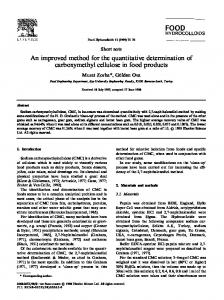
I. INTRODUCTION RF network measurements require taking a small percentage of the incident and reflected waves. This is usually done with distributed couplers. Since the 60’s, many researches have been performed in order to improve these couplers. The goal was to reach the highest directivity, this makes sense regarding VNA technology. The main path losses of these couplers were not optimized because they are fully taken into account by VNA calibration. Up to now, these couplers are widely used in measurement setups, even for load-pull measurements. Another interesting trade-off is proposed here, optimizing the losses of the main path, but with a smaller directivity. We will show that this approach is very well suited for time domain load-pull. II. THE ‘WAVE PROBE’ Our proposal consists in coupling the electromagnetic fields around a blended line. Different measurements have been done with non-contacting probes, using electric and/or magnetic fields near planar circuits [1] [2]. But by a simple RF cable without its blend in the middle placed near the main line (Fig. 1), measurements of the incident wave on one extremity, and the reflected one on the other extremity, with a theoretical infinite directivity [3] are possible. In fact, the unblended part of coupler should have a “squared” symmetric form, in order to realize an optimal combination of electric and magnetic
Fig. 3.
Measured directivity of the wave probe before calibration.
The best compromise we found between directivity and coupling gives a coupling value about 40 dB (Fig. 4). Thus, we have realized a very simple kind of “wave probe”. The losses of the main blended line are smaller than 0.5 dB, including its connectors. If we compare with and without the wave probe, the wave probe induces losses smaller than 0.1 dB (this is coherent with a coupling value as low as 40 dB). In a on-wafer passive load-pull environment, the blended line is the “cable” between the mechanical tuners and the wafer probe.
important part of the tuner’s capabilities. The following equation (1) describes the “real” matching capability (Γ1) at a DUT plane with a coupler (described by [S] parameters) before a tuner (ΓT).
Γ1 = S11 +
S12 × S 21 × ΓT 1 − ΓT × S 22
(1)
An example is given with a very good tuner (ΓT = 0.95) and a perfectly adapted coupler (S11=0 and S22=0 for the coupler, it gives the equation (2)) : 2
Fig. 4. Measured coupling value for an optimal position of the RF wave probe.
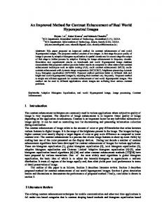
III. LOAD-PULL MEASUREMENTS REQUIREMENTS Load-pull measurements used to be performed with power meters, but now VNAs are frequently used, and the very new systems are based on the LSNA (Large Signal Network Analyzer). With the VNA, the phase information is available frequency per frequency, and with the LSNA we get absolute phases and absolute amplitudes of fundamental and harmonic frequencies, thus reaching time domain waveforms. The impedance matching is done with mechanical tuners or active loops, some benches handle 1 or 2 harmonic impedances in addition with the fundamental one. The measurement system has to take the wave information to achieve DUT non linear characterization. So, a not obvious question is the localization of the wave measurement component. Two different schemes are possible (at both sides of the DUT) : 1) DUT – tuner – coupler. 2) DUT – coupler – tuner. As the first choice corresponds to the tuner placed at the closest of the transistor’s terminal, we can dispose of the best matching capabilities. This approach is very well suited for simple power measurements. But at the second terminal of the tuner on the load side, the DUT wave information are more difficult to get and to compute, they depend on the tuner settings. Moreover, especially if the tuner handles harmonic matching, harmonic wave information detected by the coupler are extremely small. So, this configuration is not convenient for DUT time domain waveforms characterization. A less classical organization of benches consists in applying the second scheme. If we want to measure accurately the non linear waves including harmonics at DUT terminals, the best is to connect the RF coupler directly on the DUT terminals. One drawback of this method is that classical distributed couplers are heavy and relatively big, this is difficult for managing onwafer measurements. A second and more important difficulty is the losses between the DUT and the tuner. These losses on the main coupler line, usually -1.5 to -2 dB, cancel an
Γ 1 = S 21 × Γ T
.
(2)
If we take |S12| = |S21| = -1.5 dB for the losses, the best matching capabilities at the DUT planes fails to |Γ1| = 0.48, this is a very poor load-pull tuning performance. IV. APPLICATION OF THE ‘WAVE PROBE’ TO LOAD-PULL MEASUREMENTS So, we propose a third choice : 3) DUT – Blended Line with ‘wave probe’ – tuner. With our coupling method, we can benefit of the advantages of the two previous cases. Best load-pull environments are using a small solid low-loss blended line between the RF wafer probe and the tuner. The presence of the blended line offers an opportunity to insert our ‘wave probe’. Table I sums up the different configurations. There is as such no further need to insert a separate coupler. So, we only have the losses of the blended line (the – 40 dB coupling can be neglected). The losses of this high quality line are smaller than 0.5 dB, so we can reach at least |Γ1| ≥ 0.75 (compared with the |Γ1| = 0.48 previously found) in the DUT plane. As we can observe in Fig. 3, the coupling factor slowly increases with the frequency. We get an interesting compensation as the signal magnitude decreases when the frequency increases (passive devices as cables or connectors have more losses if frequency increases and harmonic levels are smaller). This property balances the measurement sensibility in all the considered bandwidth of frequencies. Moreover, a coupling factor close to 40 dB is not a problem for high power device measurement (> 30 dBm), as the measurement inputs of network analyzers usually allow up to –10 dBm : we will limit the use of step attenuators. The main drawback of our ‘wave probe’ is its smaller directivity, compared to classical distributed couplers. Our coupling system is used to feed the A and B inputs (incident and reflected waves) into a LSNA (Fig. 5). It is important to notice that all following measurements are based on a coaxial calibration. The first presented
TABLE I SUMMARY OF DIFFERENT CONFIGURATIONS OF BENCHES DEDICATED TO LOAD-PULL MEASUREMENTS 1) DUT- Tuner- Coupler
2) DUT - Coupler – Tuner
/
-
/
-
-
-
-
.
S11 (opposite of directivity) (dB)
measurement with our LSNA is a relative calibration (as a VNA). We have connected our coupler on terminal 1, and a reference HP 11692D reflectometer on terminal 2. We succeeded in obtaining calibrated directivity values on Fig. 6 by measuring the S11 (Fig. 6a) and the S22 (Fig. 6b) when 50 Ohm loads are connected. The VNA mode allows to get a huge number of frequency points. -30 -35
absolute magnitude calibration with a power meter, and second with an absolute phase calibration using an harmonic phase reference [4]). 40 35 30 25 20 wave probe
15 10
-40
5
-45
0
coupler HP 11692D
2
-50
4
6
8
10
12
14
16
18
frequency (GHz) 2
200
400
600
800
18
frequency (GHz)
Fig. 6a. Wave probe directivity with a VNA-mode calibrated LSNA (Port 1)
S22 (opposite of directivity) (dB)
3) DUT - Wave Probe - Tuner
-
directivity (dB)
Tuning Capabilities Nonlinear / Harmonic Wave Information Wave Directivity Before Calibration
-35 -40 -45 -50 -55
Fig. 7. Comparison of measured directivity : the wave probe and a HP 11692D reflectometer, LSNA large signal calibration.
This calibration is done on terminal 1 with our coupler and on terminal 2 with the coupler HP 11692D. We have used our coupler to receive absolute information (phase and amplitude) during the calibration. The Fig. 7 shows results of measurements after calibration when 50 Ohm loads are connected. The fundamental frequency was 2 GHz, and we measured the directivity on the two terminals at this frequency and harmonics until 18 GHz. The thin curve is obtained with our coupler, and the bold curve with the HP 11692D. So, the Fig. 6 and Fig. 7 show that thanks to VNA or LSNA standard calibration algorithms, we can achieve an accurate calibrated result presenting a directivity close to 35 dB.
-60
V. CONCLUSION 2
200
400
600
800
18
frequency (GHz)
Fig. 6b. HP 11692D reflectometer directivity with a VNA-mode calibrated LSNA (Port 2)
A second measurement is given here, when applying an absolute calibration SOLT (classical SOLT added first with an
We have shown the improvements generated by a new coupling method for load-pull measurements. With a simple localized wideband structure, we dispose of an innovative signal ‘wave probe’ to achieve accurate non linear device characterization. This approach give us the closest non linear information, without inducing losses ; thus we keep a good impedance tuning capability. This coupling method and these
results are offering us new possibilities for non linear time domain measurements of high power mismatched devices. ACKNOWLEDGEMENT The authors wish to acknowledge the DGA/D4S/MRIS for their financial support, and the common laboratory THALESIRCOM (MITIC).
[2] S. Osofsky, S. E. Schwarz, “Design and Performance of a NonContacting Probe for Measurements on High-Frequency Planar Circuits”, IEEE Transactions on MTT, Vol 40, N°8, August 1992. [3] P.P. Lombardini, R.F. Schwartz, P.J. Kelly, “Criteria for the Design of Loop-Type Directional Couplers for the L Band”, IRE Transactions on MTT, October 1956. [4] J. Verspecht, “Calibration of a Measurement System for Nonlinear Devices”, Ph.D. Thesis, Vrije Universiteit of Brussels, November 1995.
REFERENCES [1] J. Stenarson, K. Yhland, C. Wingqvist, “An In-Circuit Noncontacting Measurement Method for S-Parameters and Power in Planar Circuits”, IEEE Transactions on MTT, Vol. 49, N°12, December 2001.
Fig. 1.
Fig. 2.
Scheme and photographs of the wave probe near RF blended line.
A
B
C
D
Electric field for incident (A) and reflected (B) wave ; Magnetic field for incident (C) and reflected (D) wave.
LSNA A1 B1
B2 A2
load
tuner Fig. 5.
DUT
harmonic tuner
Low losses Load-Pull bench organization scheme with full nonlinear information.