An SDRAM Controller Optimized for High Definition Video Coding Application Jiayi Zhu, Peilin Liu, Dajiang Zhou Department of Electronic Engineering Shanghai Jiao Tong University Shanghai, 200240, China Email:
[email protected] Abstract—The huge SDRAM bandwidth requirement is an architectural bottleneck of video decoders. Besides the large amounts of data transmission cycles, many extra overhead (up to over 50%) are incurred by the ACTIVE or PRECHARGE (A\P) operations in conventional SDRAM controllers. In this paper, we propose an optimized SDRAM controller, which can improve the bandwidth efficiency by eliminating most of the extra overhead. An access management scheme that enables consecutive data transmission is employed to reduce the need of A\P operations. In addition, a scheduler is designed to hide the latency for A\P operations. Experimental result shows that the SDRAM controller is able to meet the bandwidth requirement of real-time decoding 1080P H.264 video streams, at less than 100Mhz with 32-bit DDR SDRAM.
I. INTRODUCTION High definition video decoder requires huge amount of data to be transferred with SDRAM, while accessing SDRAM is a little complicate. Under certain circumstances, ACTIVE or PRECHARGE (A\P) command shall be issued before accessing SDRAM, which may incur a lot of extra overhead cycles, thus decrease the data transmission efficiency greatly. Many researches have been undertaken in this field. Hansoo used an array address-translation technique to utilize some video processing characteristics [5] to obtain high bandwidth Tetsuro proposed a memory arbitration algorithm [3] to achieve high bandwidth. Both of them did their work to reduce unnecessary A\P by allocating memory reasonably for stored images In this paper, we propose an SDRAM controller which employs an access management scheme that enables consecutive data transmission. In addition, a scheduler used in the controller is designed to hide the latency for A\P operations. Experimental result shows that the SDRAM controller is able to meet the bandwidth requirement of realtime decoding 1080P H.264 video streams, at less than 100 MHz with 32-bit DDR SDRAM. The rest of this paper is organized as the follows. In section II, the memory accessing characteristics of various agents in a video decoder are illustrated, which derive the
978-1-4244-1684-4/08/$25.00 ©2008 IEEE
proposed access management scheme. In section III, the characteristics of SDRAM are illustrated, which derive the proposed scheduling strategy. The hardware architecture to implement the scheduling strategy is discussed in section IV. Experimental result is presented in section V. Finally, some conclusions are presented in section V. II.
PROPOSED ACCESS MANAGEMENT SCHEME
In this section, the memory accessing characteristics of various agents in a video decoder are illustrated. We find that it is frequent for the decoder to access continuous region of a stored image, which inspire us to establish an accesses management scheme that enables consecutive data transmission. 64 bit data (AU Access Unit) is transferred between the decoder and SDRAM when 32 bit DDR SDRAM is used. One AU is accessed by a burst unit, which is an access to SDRAM whose burst length is set to 2. Under this circumstance, one READ or WRITE (R\W) command accesses one AU. Since the width of one AU is 64 bit, we group the neighboring 8 samples in horizontal direction into one AU, thus the luma component of a macroblock, is composed of 16x2 AUs as shown in Figure 1. In the video decoder, three agents occupy around 95% of the total bandwidth need. They are reading reference picture (RRP) agent, loopfilter agent and display agent. RRP agent occupies the most bandwidth need. So prefetch or cache strategy is generally used to minimize its bandwidth need as much as possible. The prefetch or cache behavior is highly dependent on the content of pictures to be decoded. So the characteristics of RRP accessing memory are difficult to predict. Loopfilter agent has regular access form. For the luma component of a macroblock, it needs to read 8 AUs from the above macroblock for filtering and to write 40 AUs into the SDRAM after filtering as shown in Figure 1. Display agent has also very regular access form. It reads pixels in a picture by raster scan order, so240 consecutive AUs (1920pixels) at most may be read in one time.
3518
Authorized licensed use limited to: WASEDA UNIVERSITY. Downloaded on October 10, 2008 at 22:23 from IEEE Xplore. Restrictions apply.
consecutive AUs containing the wanted AU, which wastes the precious bandwidth. III.
Figure 1. the access charecteristic of loopfilter
Based on the fact that display and loopfilter agents access multiple consecutive AUs in either horizontal or vertical direction, we propose a scheme to describe the set of AU to be accessed by combining multiple consecutive AUs in horizontal or vertical direction into one transaction, which is described by the information including the address of first AU in this transaction (ADDR), the address increment in units of AU (INC) and the number of AU included in the transaction (NUM). Agents tell the SDRAM controller which AUs are wanted by sending the information of a transaction, i.e. ADDR, INC and NUM, which can specify the set of AU to be accessed flexibly to meet various agents’ access requirement as shown in Figure 2.
PROPOSED SCHEDULING STRATEGY
In this section, the characteristics of SDRAM are illustrated, which shows that it is possible to hide the latency by issuing A\P command as early as possible. When we access SDRAM, A\P commands are sometimes necessary before R\W commands, which incur overhead cycles named as tPR and tRCD. These overhead cycles may greatly lower the data transmission efficiency as the simple example shown in Figure 3. In this example, 5 AUs are supposed to be read from SDRAM and the last AU is supposed to reside in the same bank but in different row with the previous 4 AUs. So a PRECHARGE command and an ACTIVE command are required before the last read command. Under this case, 11 cycles are spent to transfer these 5 AUs, and the data transmission efficiency is only 45%, as is shown in Figure 3.
Figure 3. issuing SDRAM commands in order
Fortunately, we can hide the overhead cycles by scheduling SDRAM commands through exploring the multibank architecture of SDRAM. Consider the example mentioned above, if the A\P commands are issued in a proper moment, tRP and tRCD are hidden and in this case, 5 AUs are transferred in only 7 cycles with data transmission efficiency 71.4%, as is shown in Figure 4.
Figure 4. issuing SDRAM commands out of order Figure 2. various image access modes
The conventional scheme to access an image is using burst mode, with the burst length set to be 2, 4 or 8. The proposed scheme outperforms the conventional scheme in 2 aspects. Firstly, it allows agents to access much more AUs for one time. For example, the loopfilter may request to access 20 AUs in one transaction, while with conventional scheme, loopfilter can only request to access 4 AUs at most in one burst because the maximum burst length is 8. If more than 4 AUs in the transaction reside in the same bank and same row, the data transmission efficiency is improved. Secondly, the proposed scheme is more flexible than the conventional scheme. When we use the conventional scheme, it is prone to believe that set burst length to 8 will be helpful to get high data transmission efficiency. But the flexibility is lost. For example, if only 1 AU is needed, we still must access 4
With the observation that issuing A\P commands in advance can reduce overhead cycles, we propose a scheduling strategy which tries to find and issue A\P command in current or following transactions as early as possible.
Figure 5. command queue of a transaction which can’t be scheduled
According to last section, transaction describes a set of AU to be accessed and one AU is accessed by one R\W command. So transaction can be regarded as a queue of R\W command, as is shown in Figure 5. In addition to the R\W commands, some A\P commands are needed to complete the transaction. The relative order of R\W commands in a command queue is fixed, i.e. no R\W command can be brought forward before any other R\W command. But
3519
Authorized licensed use limited to: WASEDA UNIVERSITY. Downloaded on October 10, 2008 at 22:23 from IEEE Xplore. Restrictions apply.
whether one A\P command can be brought forward before certain R\W command depends on the pattern of the command queue. If there is only one A\P command included in the queue of the transaction, and it is before the first R\W command, then the order of the A\P command is also fixed, as is shown in Figure 5. Otherwise, the A\P command may be brought forward before certain R/W commands, as is shown in Figure 6.
issued for each sub transaction in order and whether it could be issued without influencing the correctness of the accessing process. If the answer is yes, the A\P command is issued. Otherwise, the commands in the first sub-transaction are issued by order. The idea of this scheduling strategy is to find and then to issue the A\P command as early as possible, which allow the following R\W commands to overlap the latency incurred by A\P command, as is shown in Figure 4. IV.
PROPOSED SCHEDULER ARCHITECTURE
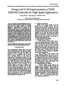
In this section, we propose our hardware architecture for the scheduler module in the SDRAM controller as shown in Figure 9. Figure 6. command queue of a transaction which can be scheduled
The pattern of a transaction command queue depends on the set of AU to be accessed and memory allocation for these AUs. We adopt the memory allocation scheme to store an image proposed in [5] as shown in Figure 7. It is possible for a transaction to cross the boundary between banks and rows and the A\P commands occur when the transaction crosses the boundary. In order to schedule commands in one transaction, we divide transaction into sub-transactions as shown in Figure 7. The so called sub-transaction is also a combinations of multiple AU, which can be regarded as a special kind of transaction that all the AU within it reside in the same bank and in same row, which means that there is only one A\P at most included in a sub-transaction and it is always before the first R\W command if available, as is shown in Figure 5.
Figure 7.
(sub)-transaction pattern and the memory allocation for image
The number of sub-transaction included in one transaction is not fixed. If there is only one sub-transaction included, no scheduling can be done within the transaction. To explore the possibility to schedule commands between transactions, multiple transaction can be divided to generate more subtransaction for scheduling, as is shown in Figure 8.
Figure 8. generation of sub-transaction
The scheduling strategy is as the follows: On every cycle, we firstly check whether there exists A\P command to be
Figure 9. proposed SDRAM controller architecture
The scheduler contains two sub-modules named as register piles (RP) and finite state machine (FSM). RP is composed of several transaction slots (TSs) and sub-transaction slots (STSs), which is used to register the information of (sub-)transaction. The information includes ADDR, INC and NUM. The information in TS is parsed to generate sub-transaction (ST), whose information is sent to STS until all the STS are filled or no more ST is available to send. Suppose there are 3 STS, ST1 is processed prior to ST2, and ST2 is processed prior to ST3. If ST1 is finished, its information will be shifted out of STS1, in the meanwhile information of ST2 and ST3 will be shifted into STS1 and STS2 respectively. Moreover the information of a new ST will be shifted into STS3 if available. The information of all STs is sent to FSM. FSM is used to decide what commands to issue and the order they are issued. There are nine states in the FSM as shown in Table I. When current state of FSM is ACTx or PREx states, the A\P command is issued to the bank and row specified in STx; when current state of FSM is READ or WRITE state, the R\W command is issued to the column specified in ST1; when current state of FSM is IDLE state, no command is issued. Every cycle, the FSM transits between states according to the information from the STS and the state of SDRAM but regardless of which state the FSM was last cycle. The transition condition used by the FSM is listed as the follows. The nine states are listed according to their priority. “STx need pre” occurs when the target bank of STx is ACTIVE, but the actived row is not the target row of STx.
3520
Authorized licensed use limited to: WASEDA UNIVERSITY. Downloaded on October 10, 2008 at 22:23 from IEEE Xplore. Restrictions apply.
“STx need act” occurs when the target bank of STx is idle. ”STx_bank_unused” occurs when STx’s target bank is different from all the previous ST’s bank.
are decoded in one second under 550MHz. The data transmission efficiency is only 18%. TABLE III.
TABLE I. State
Condition
PRE1
ST1_need_pre
ACT1
ST1_need_act
PRE2
ST2_need_pre & ST2_bank_unused
ACT2
ST2_need_act & ST2_bank_unused
PRE3
ST3_need_pre & ST3_bank_unused
ACT3
ST3_need_act & ST3_bank_unused
READ
ST1_is_read_access
WRITE
ST1_is_write_access
IDLE
na
V.
1
Proposed
conventional
Efficiency
77%
18%
Frequency
95MHz
550MHz
The proposed SDRAM controller has been implemented by verilog on Xilinx FPGA Vertex4 XC4VLX100 speed -10. Report shows that the synthesizable frequency is 140MHz and resource consumption is 1160 luts. VI.
EXPERIMENTAL RESULT
In order to verify the performance benefit brought by the proposed access management scheme and scheduling strategy, a SDRAM controller which use conventional burst access scheme is used for comparison. We do the behavioral simulation of the HP H.264 video decoder on modelsim to find the lowest frequency under which the input 1080P bitstream can be decoded at 30fps. The off-chip memory is 32-bit DDR SDRAM. The interval between I frames in this sequence is 15. There are 14 P and B frames respectively in the sequence in the form of IPBPBPB… Statistic data are acquired during the simulation. Every 5000 cycles, the amount of data transmitted between decoder and SDRAM and the cycles in which the SDRAM controller is busy (i.e. the transaction slots are occupied) is recorded. The amount of data transferred between SDRAM and various agents for 30 frames (bandwidth requirement) is as the follows. TABLE II.
COMPARISON WITH ALTERA REFERENCE MODEL
FSM TRANSITION CONDITION
BANDWIDTH OF VARIOUS AGENTS
In this paper, we propose a high performance SDRAM controller optimized for video application. Firstly, we combine multiple access units into one transaction to enable consecutive data transmission, which suits the characteristics of video decoder accessing. Afterwards, we apply the scheduling strategy that finds and issues the A\P command as early as possible to allow the latency incurred to be overlapped. Moreover, hardware architecture for scheduler is proposed. Experimental result shows that the SDRAM controller is able to meet the sbandwidth requirement of realtime decoding 1080P H.264 video streams, at less than 100 MHz with 32-bit DDR SDRAM. REFERENCES [1]
[2]
[3]
[4]
[5]
Agents
Ref Pic
Display
Loogfilter
Misc
Total
Bandwidth
214MB
90MB
135MB
22MB
461MB
When we use the proposed SDRAM controller in the decoder, 30 frames are decoded in one second under 95MHz. The data transmission efficiency defined as the ratio of the number of cycles in which data are transmitted and the number of cycles in which the SDRAM controller is busy (i.e. the transaction slots are occupied) is 77%. When we use the conventional SDRAM controller in the decoder, 30 frames
CONCLUSION
[6]
[7] [8]
Joint Video Team, Draft ITU-T Recommendation and Final Draft International Standard of Joint Video Specification, ITU-T Rec.H.264 and ISO/IEC 14496-10 AVC, May 2003. Takizawa, T.; Tajime, J.; Harasaki, H.; “High performance and cost effective memory architecture for an HDTV decoder LSI” ICASSP '99. Proceedings. Page(s):1981 - 1984 vol.4 Takizawa, T.; Hirasawa, M.; “An efficient memory arbitration algorithm for a single chip MPEG2 AV decoder” IEEE Transactions on Consumer Electronics, Aug. 2001 Page(s):660 - 665 Kim, H.S.; Vijaykrishnan, N.; Kandemir, M.; Brockmeyer, E.; Catthoor, F.; Irwin, M.J.; “Estimating influence of data layout optimizations on SDRAM energy consumption” ISLPED '03. Proceedings, Page(s):40 - 43 Hansoo Kim; In-Cheol Park; “High-performance and low-power memory-interface architecture for video processing applications” IEEE Transactions on Circuits and Systems for Video Technology, Nov. 2001 Page(s):1160 - 1170. Hong-Kai Chang; Youn-Long Lin; “Array allocation taking into account SDRAM characteristics” Proceedings of the ASP-DAC 2000, Page(s):497 – 502 Panda, P.R.; Dutt, N.D.; “Reducing address bus transition for low power memory mapping” ED&TC 96. Proceedings Page(s):63 - 68 Micron Double Data Rate SDRAM MT46V32M4, MT46V16M8, MT46V8M16 datasheet, www.micron.com
3521
Authorized licensed use limited to: WASEDA UNIVERSITY. Downloaded on October 10, 2008 at 22:23 from IEEE Xplore. Restrictions apply.