Journal of the Korean Physical Society, Vol. 51, No. 4, October 2007, pp. 1378∼1382
Annealing Effect on the Electrical and the Optical Characteristics of Undoped ZnO Thin Films Grown on Si Substrates by RF Magnetron Sputtering Do Kyu Lee, Sung Kim, Min Choul Kim, Sung Hwan Eom, Hyoung Taek Oh and Suk-Ho Choi∗ Department of Physics and Applied Physics, Institute of Natural Sciences, Kyung Hee University, Yongin 449-701 (Received 11 June 2007) Undoped ZnO films have been grown on Si wafers by RF-magnetron sputtering and have been characterized as a function of annealing temperature (Ta ) by employing X-ray diffraction, photoluminescence (PL), and Hall effect measurements. The samples were annealed from 500 to 1000 ◦ C for 3 min under an oxygen ambient in a rapid thermal annealing apparatus. The ZnO films consisted of (100) and (002) polycrystals, and their relative portion changed with varying Ta . After annealing at Ta ∼ 800 ◦ C, the (100) polycrystals dominantly existed, and the near-band-edge PL peak was most intense, whilst the n-type character was most weakened. We propose that native structural defects play a key role in enhancing the n-type character of ZnO films, judging from the close correlation between the relative intensity of the bound-exciton-related PL lines and the Hall parameters as a function of Ta . PACS numbers: 78.55.Et, 78.66.Hf, 73.61.Ga Keywords: ZnO films, Photoluminescence, Sputtering, Annealing, Hall effect, X-ray diffraction
I. INTRODUCTION In the last decade, ZnO has received much attention in view of optoelectronic device applications in the ultraviolet and the visible ranges due to its prominent properties, such as wide band gap (3.37 eV) and high exciton binding energy (60 meV) [1–3]. ZnO is also used in a polycrystalline form for facial powder, piezoelectric devices, varistors, phosphors, and transparent conducting films [1]. ZnO films can be easily deposited on GaN substrates because GaN has a wurtzite crystal structure and because the lattice mismatch between the two materials is only 1.8 % [4]. Despite such excellent properties, it is difficult to determine the doping type (n or p) of undoped ZnO films by nature due to their native defects or unintentional H atoms as shallow donor [5–7]. The n-type character of ZnO films can be enhanced by doping with group-III elements such as Al, Ga and In [6]. Group-V elements such as N, P, As and Sb have been tried extensively as p-type dopants, but it has proven difficult to do p-type doping in ZnO only with the GroupV group elements [7]. Recently, efforts have been made to obtain p-type ZnO by the co-doping of an acceptor (N) and a donor (Al, Ga) [7–9]. Due to the difficulties of p-type doping, p-n heterojunction devices have been studied, but they have intrinsic problems of strain and ∗ E-mail:
[email protected]
lattice mismatch at the interfaces. Recently, as p-type doping has become partly successful, a number of studies on homojunction ZnO devices have been reported [8–10]. On the other hand, the intrinsic properties of ZnO have also been improved by controlling their preparation conditions [11–13]: for example, p-type conductivity can be obtained in undoped ZnO by only adjusting the oxygen partial pressure in the sputtering plasma, affecting the density of the native oxygen defects. These results suggest that more things have to be done to improve intrinsically ZnO films before doping by adjusting several preparation conditions. In this paper, we report systematic studies on annealing behaviors of undoped ZnO films that were fabricated by RF magnetron sputtering. We investigated their optical and electrical characteristics as functions of annealing temperature, and we will discuss the experimental results based on possible physical mechanisms.
II. EXPERIMENT The ZnO powder was sintered at 650 ◦ C for 2 h under vacuum at a pressure of 3 × 10⁻⁶ Torr to make ZnO sputtering targets. The targets were then mounted in a RF magnetron sputtering system to deposit ZnO films on p-type Si (100) substrates. Prior to use, the substrates were vibrated ultrasonically first in acetone and then in
-1378-
Annealing Effect on the Electrical and the Optical Characteristics· · · – Do Kyu Lee et al.
-1379-
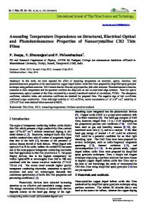
Fig. 2. XRD patterns of ZnO films as a function of annealing temperature. The intensities of two XRD peaks representing the (100) and the (002) crystal planes, respectively, of ZnO are shown in the inset.
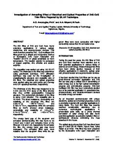
Fig. 1. (a) Dependence of room-temperature PL spectra of ZnO films on annealing temperature. (b) The relative intensities of the near-band-edge (NBE), oxygen vacancy (VO ), oxygen interstitial (Oi ), and oxygen antisite (OZn ) PL emissions as a function of annealing temperature.
alcohol and finally were rinsed in deionized (DI) water. After the system had been evacuated to a base pressure of 3 × 10⁻⁶ Torr, the substrates were pre-sputtered at a power of 50 W for 10 min. The ZnO sputtering was done for 50 min at a working pressure of 10−3 Torr and the preparation conditions are as follows: RF power: 70 W, deposition rate: 2 nm/min, and gas mixing ratio of O2 /Ar: 1/8. Rapid thermal annealing (RTA) was done in an oxygen ambient at a pressure of 1 Torr by changing annealing temperature (Ta ) from 500 to 1000 ◦ C for 3 min in steps of 100 ◦ C. The crystal structure of the ZnO films was investigated by using an X-ray diffractometer, and their thicknesses were measured by using a surface profiler (alpha
step IQ). Photoluminescence (PL) spectroscopy was employed for optical characterization of the ZnO films. The PL spectra were measured in a closed-cycle refrigerator by using the 325 nm line of a HeCd laser as the excitation source. Emitted light was collected by using a lens and were analyzed using a grating monochromator and a GaAs photomultiplier (PM) tube. Standard lock-in detection techniques were used to maximize the signalto-noise ratio. The laser power for the PL excitation was about 3 mW. Hall-effect measurements were performed in an apparatus (Echopia model HEM-2000) by using the van der Pauw method. For Ohmic contacts, an In film of 500 µm in diameter was deposited on the ZnO film by using a shadow mask in a thermal evaporator and was subsequently annealed at 300 ◦ C for 10 min. The intensity of the B field was 0.37 T, and the current was varied from 0.1 µA to 10 mA. All Hall measurements were done in a dark room to exclude unwanted ambient light.
III. RESULTS AND DISCUSSION Figure 1(a) shows the dependence of the roomtemperature PL spectra of ZnO films on the annealing temperature (Ta ). The PL bands at ∼3.3 and ∼2.4 eV are usually attributed to the near-band-edge (NBE) emission and the oxygen-related deep level (DL), respectively [14,15]. The DL PL band consists of 3 major peaks, 1.62, 2.28 and 2.38 eV, originating from oxygen vacancies (VO ), oxygen interstitials (Oi ), and oxygen antisites (OZn ), respectively [16]. The relative intensities of the four PL peaks depend on the annealing temperature as shown in Figure 1 (b). The intensity of the NBE peak
-1380-
Journal of the Korean Physical Society, Vol. 51, No. 4, October 2007
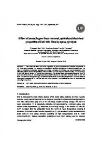
Fig. 3. (a) Resistivity, (b) Hall coefficient, (c) electron carrier concentration and (d) Hall mobility as functions of annealing temperature.
increases from Ta = 500 to 900 ◦ C, but above 900 ◦ C, it decreases. The VO peak shows almost no change in its intensity over the full range of Ta , whilst the intensities of the Oi and the OZn peaks increase above 900 ◦ C. Figure 2 shows X-ray diffraction (XRD) patterns of ZnO films as a function of Ta . Two XRD peaks representing (100) and (002) crystal planes [17] are observed at 2θ = ∼32.7◦ and ∼34.2◦ , respectively, over the full range of Ta . The annealing behaviors of both peak intensities are summarized in the inset of Figure 2. The intensity of the (100) peak has a maximum at around Ta = 800 ◦ C, whilst the intensity of the (002) peak shows a gradual increase with increasing Ta . These results indicate that after annealing above 500 ◦ C, the ZnO films consist of polycrystals with two dominant crystal planes of (100) and (002), as suggested before [18], and that the relative portion of the crystallites with each orientation changes with Ta . Figure 3 (a), (b), (c) and (d) show the resistivity (ρ), the electron carrier concentration (Ne ), the Hall mobility (µ), and the Hall coefficient (Rh ), respectively as functions of Ta , which were obtained from the Hall effect measurements. At around 800 ∼ 900 ◦ C, the ρ, µ and Ne values are the smallest, and the Rh is the largest (close to zero), suggesting that the ZnO films are mostly n-type, except for the temperature range, in which they are almost neutral. It is noted that the (100) polycrystals are most dominant and that the NBE PL is the strongest at similar temperatures, as shown in Figure 1 and 2. This indicates that ZnO film becomes less n-type with its NBE PL being stronger as the portion of (100) polycrystals increases. Figure 4 (a) shows ultraviolet PL spectra that are more detailed because they were measured at 15 K. The PL
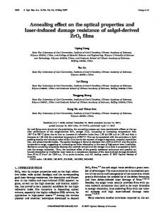
lines resolved from the spectra originate mostly from bound-exciton-related recombinations followed by longitudinal optical (LO) phonon replicas with an energy separation of 72 meV [19, 20]. The PL peak at 3.363 is widely known to be due to excitons bound to neutral donors (D0 X) [20]. Previously, two interesting PL peaks (3.332 and 3.312 eV) had been observed at 10 K in single-crystalline ZnO and had been attributed to excitons bound to structural defects [19]. He et al. also found a similar PL emission at 3.315 eV and named it as an A line [21]. In this work, the A line is observed at 3.336 eV after annealing at Ta = 500 ◦ C, and as shown in Figure 4 (b), it is redshifted to 3.303 eV as Ta increases from 500 to 1000 ◦ C, possibly resulting from structural reorientations caused by the annealing. The PL peak at 3.327 eV is observed only after annealing at 1000 ◦ C in this work. This peak is thought to originate from the two-electron satellite (TES) transition, which involves radiative recombination of an exciton bound to a neutral donor, leaving the donor in the excited state [19]. First, second, and third LO phonon replicas of the TES are also observed at 3.264, 3.197 and 3.128 eV, respectively, as marked in Figure 4 (a). Figure 4 (c) shows Ta -dependent integrated intensities of the two dominant PL lines, A and D0 X. Their relative intensities, I(A)/I(D0 X), are minimum at around 800 ◦ C. As reported before [12, 13], ZnO can be an nor a p-type semiconductor even without doping due to native defects such as oxygen and zinc vacancies. We propose that the structural defects responsible for the A line play a key role in enhancing the n-type character of our samples, which is consistent with the fact that the ZnO films are almost neutral after annealing at around 800 ◦ C, as shown in Figure 3.
Annealing Effect on the Electrical and the Optical Characteristics· · · – Do Kyu Lee et al.
-1381-
Fig. 4. (a) Resolved PL spectra at 15 K for the ZnO film annealed at 1000 ◦ C. (b) Annealing-temperature-dependent PL spectra measured at 15 K. (c) Integrated PL intensities of A and D0 X PL lines, and their ratio as a function of annealing temperature.
IV. CONCLUSION X-ray diffraction, PL, and Hall effect measurements were employed to study annealing behaviors of undoped ZnO films grown on Si wafers by RF-magnetron sputtering. Annealing was done from 500 to 1000 ◦ C for 3 min under an oxygen ambient in a rapid thermal annealing apparatus. The ZnO films consisted of (100) and (002) polycrystals, and their relative portion strongly depended on Ta . After annealing at Ta ∼ 800 ◦ C, the (100) polycrystals were most dominant, and the NBE PL peak was most strong, whilst the n-type character was most weakened. We suggest that native structural defects are responsible for determining the n-type character of ZnO films, which was confirmed by the close correlation between the relative intensity of the bound-exciton-related PL lines being dominant at 15 K and the Hall parameters as a function of Ta . ACKNOWLEDGMENTS This work was supported by a Korea Research Foundation (KRF) Grant funded by the Korean Government (Ministry of Education & Human Resources Development, Basic Research Promotion Fund) (KRF-200610025-C00041). REFERENCES [1] D. C. Reynolds, D. C Look, B. Jogai and H. Morkoc Solid State Commun. 101, 9 (1997).
[2] J. Lee, W. Choi, C. Kim, J. Hong, T.-U. Nahm and H. Cheong, J. Korean Phys. Soc. 49, 1126 (2006). [3] R. Navamathavan, J.-H. Lim, D.-K. Hwang, B.-H. Kim, J.-Y. Oh, J.-H. Yang, H.-S. Kim, S.-J. Park and J.-H. Jang, J. Korean Phys. Soc. 48, 271 (2006). [4] D. C. Look, Mater. Sci. Eng. B 80, 383 (2001). [5] D. C. Look, J. W. Hemsky and J. R. Sizelove, Phys. Rev. Lett. 82, 2552 (1999). [6] Gang Xiong, John Wilkinson, Brian Mischuck, S. Tuzemen, K. B. Ucer and R. T. Williams , Appl. Phys. Lett. 80, 1195 (2002). [7] A. Y. Polyakov, N. B. Smirnov, A. V. Govorkov, A. I. Belogorokhov, E. A. Kozhukhova, A. V. Markov, A. Osinsky, J. W. Dong and S. J. Pearton , Appl. Phys. Lett. 90, 132103 (2007) [8] M. Joseph, H. Tabata, H. Saeki, K. Ueda and T. Kawai, Physica B 302/303, 140 (2001). [9] K. Nakahara, H. Takasu, P. Fons, A. Yamada, K. Iwata, K. Matsubara, R. Hunger and S. Niki, Appl. Phys. Lett. 79, 4139 (2001). [10] Z. P. Wei, Y. M. Lu, D. Z. Shen, Z. Z. Zhang, B. Yao, B. H. Li, J. Y. Zhang, D. X. Zhao, X. W. Fan and Z. K. Tang , Appl. Phys. Lett. 90, 042113 (2007). [11] G. Xiong, J. Wilkinson, B. Mischuck, S. Tuzemen, K. B. Ucer and R. T. Williams, Appl. Phys. Lett. 80, 1195 (2002). [12] Y. Ma, G. T. Du, S. R. Yang, Z. T. Li, B. J. Zhao, X. T. Yang, T. P. Yang, Y. T. Zhang and D. L. Liu, J. Appl. Phys. 95, 6268 (2004). [13] M.-S. Oh, S.-H. Kim and T.-Y. Seong, Appl. Phys. Lett. 87, 122103 (2005). [14] F. K. Shan, G. X. Liu, W. J. Lee and B. C. Shin, J. Appl. Phys. 101, 053106 (2007). [15] X. T. Zhang, Y. C. Liu, L. G. Zhang, J. Y. Zhang, Y. M. Lu, D. Z. Shen, W. Xu, G. Z. Zhong, X. W. Fan and X. G. Kong, J. Appl. Phys. 92, 3293 (2002).
-1382-
Journal of the Korean Physical Society, Vol. 51, No. 4, October 2007
[16] B. Lin, Z. Fu and Y. Jia, Appl. Phys. Lett. 79, 943 (2001). [17] Z. Z. Zhi, Y. C. Liu, B. S. Li, X. T. Zhang, Y. M. Lu, D. Z. Shen and X. W. Fan, J. Phys. D 36, 719 (2003). [18] T. A. Polley and W. B. Carter, Thin Solid Films 384, 2,(2001). ¨ Ozg¨ ¨ ur, S. Doan, X. Gu, H. Morkoc, B. [19] A. Teke, U. Nemeth, J. Nause and H. O. Everitt, Phys. Rev. B 70,
195207 (2004). [20] B. K. Meyer, H. Alves, D. M. Hofmann, W. Kriegseis, D. Foster, F. Bertram, J. Christen, A. Hoffmann, M. Strassburg, M. Dworzak, U. Haboeck and A. V. Rodina, Phys. Status Solidi B 241, 231 (2004). [21] H. P. He, H. P. Tang, Z. Z. Ye, L. P. Zhu, B. H. Zhao, L. Wang and X. H. Li, Appl. Phys. Lett. 90, 023104 (2007).